Note: Descriptions are shown in the official language in which they were submitted.
CA 02593216 2007-07-06
HARTING Electronics GmbH & Co. KG
Marienwerderstraf3e 3 2007-06-20
D-32339 Espelkamp P206-11 CA P 9
PRESSURE GUIDE FOR PCB
BACKGROUND OF THE INVENTION
1. Field of the Invention
The invention pertains a pressure guide for a printed circuit board that can
be inserted between two guide bars in a circuit board connector housing in
order to achieve precise contacting of the strip conductors applied to the cir-
cuit board with corresponding electric contacts arranged in an edge connec-
tor.
A device of this type is required for ensuring the exact mechanical locating
of
contact decks arranged on a circuit board relative to electric contacts
located
in an edge connector.
2. Description of the related art
General direct plug-and-socket connections between circuit boards and cir-
cuit board connectors provided for this purpose hardly cause any tolerance
problems between the contacts on the circuit board and the electric contacts
within the connector due to the relatively large contact spacing (> 1 mm).
However, if the contact spacing is reduced, increased precision is required in
the manufacture of the circuit boards such that the costs are inevitably in-
creased. Otherwise, the relatively broad manufacturing tolerances of conven-
tional circuit boards make it difficult to prevent mismating between the con-
tacts on the circuit board and the exactly located contacts in the connector.
P206-1l CA P 9.doc
CA 02593216 2007-07-06
2
SUMMARY OF THE INVENTION
Consequently, the invention is based on the objective of realizing a device of
the initially cited type in such a way that the best mechanical conformity pos-
sible is achieved between the position of the contact decks on the circuit
board and the contacts in the edge connector, namely with consideration of
the broad fault tolerances in the manufacture of circuit boards.
This objective is attained by providing a spring element that acts upon the
io narrow side of the circuit board within one of the guide bars.
The advantages attained with the invention can be seen, in particular, in that
the relatively broad dimensional tolerances that apparently cannot be re-
duced in the manufacture of the connecting region on a circuit board are
minimized by means of the inventive spring element to such a degree that it
is also possible to precisely contact socket contacts in the edge connector
that are arranged within small distances of one another.
Mismated contacts or, in extreme instances, short circuits are unavoidable if
the contacts of the circuit board are not exactly located relative to the
socket
contacts.
This is the case, in particular, if the connecting region of a circuit board
is
inserted into the mating slot of an edge connector and the circuit board is
not
definitively located relative to the connector. The reason for this can be
seen
in that dimensional tolerances also apply to the longitudinal direction of the
slot. However, if a contact spacing of < 1 mm is required, the strict
tolerances
on both sides of the mating region can no longer be guaranteed by the
manufacturers of circuit boards.
In order to be inserted into the edge connector, both sides of the circuit
board are held in a guide bar that, in turn, is snapped into a circuit board
connector housing or said housing features a bottom plate and a cover plate
P206-11 CAP 9.doc
CA 02593216 2007-07-06
3
with protruding guide webs, in which the circuit board is located similar to
guide bars.
The precise locating of the circuit board in an edge connector requires a
strict tolerance between the first contact deck on the circuit board and the
contact edge in the edge connector.
To this end, the edge connector is adjusted to a minimal height tolerance
referred to one of the two guide bars, between which the circuit board is lo-
cated.
The spring element arranged in the second guide bar has a spring arm that
is oriented in the mating direction of the circuit board.
During the insertion of the circuit board, the spring element exerts pressure
upon the narrow side of the circuit board such that a circuit board that previ-
ously could be loosely inserted between the guide bars is inserted into the
edge connector in an exactly located fashion shortly before the strip conduc-
tors are contacted with the electric contacts.
In this case, the spring element is arranged in one of the guide bars in the
form of an integral or separate element that may be realized in the form of a
plastic part or a metal part.
BRIEF DESCRIPTION OF THE DRAWINGS
One embodiment of the invention is illustrated in the figures and described in
greater detail below. The figures show:
Fig. 1 shows an aspect of a backplane with an edge connector and a circuit
board arranged between the guide bars before the mating process;
P206-11 CA P 9.doc
CA 02593216 2007-07-06
4
Fig. 2 shows a detail of Figure 1 before the mating process;
Fig. 3 shows a detail of Figure 1 after the mating process;
Fig. 4a shows an aspect of a circuit board that is inserted between a bottom
plate and a cover plate;
Fig. 4b shows a detail of the spring element according to Figure 4a;
Fig. 5a shows an aspect of a separate spring element in a cover plate, and
Fig. 5b shows a sectional representation of the spring element with an in-
serted card.
DESCRIPTION OF THE PREFERRED EMBODYMENTS
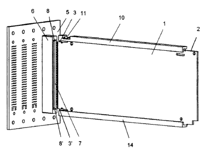
Figure 1 shows an arrangement for directly mating a circuit board 1 with an
edge connector 6 that is fixed on a so-called backplane 5.
The circuit board 1 is inserted between two guide bars 10, 14 that are usually
mounted on a not-shown cover plate or bottom plate or on corresponding
support bars.
In this case, the upper guide bar 10 features a cutout 11 that is illustrated
in
detail in Figure 2 in the immediate vicinity of the edge connector 6.
A spring element 16 is arranged within the recess 11 that extends from the
base of the U-shaped bar 10 into the lateral limbs 12, wherein the spring arm
17 of the spring element lies on the lateral limbs that are realized in the
form
of braces 13 in this case with its rounding 18. The recess is realized such
that the rounding 18 of the spring arm 17 extends into the U-shaped cutout
11 of the guide bar.
P206-11 CA P 9.doc
CA 02593216 2007-07-06
A spring element 16 made of a metallic material is inserted into the upper
guide bar 10 that is usually made of a plastic material or the spring element
is shaped out of the material of the guide bar.
5
According to Figure 3, the circuit board 1 located in the upper guide bar 10
features a step 3 on its mating side, wherein the thusly tapered front section
needs to be inserted into the mating slot 7 of the edge connector 6.
The spring arm 17 lies on the lateral braces 13 within the recess 11 until
shortly before the circuit board is inserted into the edge connector, wherein
the circuit board 1 that could previously be inserted between the guide bars
10, 14 with quite some vertical clearance is pressed against the lower guide
bar 14 as soon as the edge 4 of the circuit board 1 reaches the rounding 18
of the spring arm 17.
However, the lower guide bar 14 is adapted to the strict tolerance referred to
the lower edge 8' of the mating slot 7 in the edge connector 6 such that exact
conformity between the electric contacts in the connector and the strip con-
ductors arranged on the circuit board is ensured.
An additional improvement in locating the circuit board relative to the edge
connector is achieved in that the circuit board is pressed against the lower
edge 8' of the mating slot in the edge connector 6, wherein the lower mating
slot edge 8' of the edge connector 6 is situated in a slightly elevated
position
referred to the lower guide bar 14 (with consideration of the variations in
size
of the circuit boards).
Figure 4a shows a section of a circuit board housing in which the circuit
board is held in guide bars between a cover plate 20 and a bottom plate 24,
wherein said guide bars are formed by locating braces 21 that are shaped
out of the plate material in a handle-like fashion and point into the
interior.
P206-11 CA P 9.doc
CA 02593216 2007-07-06
6
Two adjacent locating braces that are spaced apart from one another and
arranged in the front and rear regions respectively form a guide bar for a cir-
cuit board 1 to be inserted therein.
A spring element 26 acting upon the circuit board 1 is illustrated in Figure
4b
in the form of an enlarged partial section, wherein said spring element is
shaped out of the material of the cover plate 20 and ensures that the circuit
board 1 is pressed against the bottom plate 24.
Figure 5a shows a separate spring element 30 that can be subsequently in-
stalled and therefore is suitable for retrofitting applications in a cover
plate
that does not feature an integral spring element.
For this purpose, the spring element 30 is integrated into a plastic body 31
that is mounted in two openings 25 in the cover plate 20, wherein said open-
ings consist of already provided standard openings or are produced subse-
quently.
In this case, a spring arm 32 shaped out of the plastic body 31 penetrates
into a cutout 22 that is formed by inwardly bent locating braces 21. This
means that the spring arm acts upon the upper narrow side 2 of the circuit
board 1 as shown in Figure 5b.
The plastic body 31 of the separate spring element is snapped into the open-
ings 25 provided or to be provided in the cover plate 20 by means of two in-
tegral plunger pins 33.
P206-I 1 CA P 9.doc