Note: Descriptions are shown in the official language in which they were submitted.
CA 02593340 2007-07-10
Multi-layer body with micro-optical means
15 The
invention concerns a process for the production of a multi-layer
body having micro-optical structures, a multi-layer body produced with the
process and a security document having said multi-layer body.
Numerous processes are known for enhancing the forgery-proof
nature of security documents, for example banknotes or visas.
20 EP 0 429 782 Al provides an arrangement for improving the forgery-
proof nature of banknotes, which provides an OVD film which is applied to
the banknote and which is macroscopically shaped, for example by intaglio
printing. In that procedure, a macroprofile which has at most 10 lines per
millimeter is transferred. The macroprofile and the microprofile of the OVD
25 are so matched to each other that, in attempts at forgery, minor
deviations
can be immediately detected.
WO 02/091041 Al describes a micro-mirror array which can be
transferred on to a paper or plastic material substrate by printing with ink
or lacquer. The period of the micro-mirrors is typically between 30 and 60
30 Am. The micro-mirrors can be used both in a transillumination mode
and
also in an incident illumination mode. It is possible In that way to form a
two-channel tilting image.
Now the object of the present invention is to provide a simple and
inexpensive process for the production of a multi-layer body having micro-
35 optical
structures which are in register relationship with further security
1
CA 02593340 2007-07-10
features such as OvDs and pictorial representations, as well as such a
multi-layer body.
The object of the invention is attained by a process for the
production of a multi-layer body comprising a first layer which is formed
from micro-optical structures and which at least partially covers over one or
more further layers having image regions and/or effect regions which
produce an optical effect, wherein it is provided that the micro-optical
structures are applied by means of intaglio printing to the layer under the
first layer or are introduced into the first layer.
The object is further attained by a multi-layer body comprising a first
layer which is formed from micro-optical structures and which at least
partially covers over one or more further layers having image regions
and/or effect regions which produce an optical effect, wherein it is provided
that the micro-optical structures are applied by means of intaglio printing
to the layer under the first layer or are introduced into the first layer.
The object is further attained by a security document having the
multi-layer body according to the invention.
The invention provides that micro-optical structures such as for
example micro-lens arrays or blaze gratings are applied by means of
intaglio printing. The multi-layer body can be both a transfer film which is
applied to a security document or it can be the security document itself or a
security document with a transfer film.
Because a plurality of micro-optical structures can be applied at the
same time with this process, the complication and expenditure for
orientation of the micro-optical structures in accurate register relationship
is considerably reduced because the only important consideration is for the
one or more printing plates to be oriented relative to each other prior to the
printing procedure. Thereafter the multi-layer body can be replicated in
large numbers.
In addition it is also possible for the micro-optical structures to be
applied to the multi-layer body or introduced into the multi-layer body in an
endless, repetitive pattern without being in register relationship with
further micro-optical structures.
2
CA 02593340 2014-04-04
The multi-layer body according to the invention is distinguished in
that it is possible to produce micro-optical structures which are not shaped
into a film layer. That avoids all problems which can arise when micro-
optical structures are transferred into a transfer film in a roll-to-roll
process
and then have to be transferred on to a security document in register
relationship with other features. A further advantage is that a micro-optical
structure which is formed from optical elements which are not connected
together cannot be removed and transferred without destroying the
structure. Arranging the micro-optical structures in register relationship
further enhances the forgery-proof nature of the multi-layer body according
to the invention. The multi-layer body can involve a particularly strict
register relationship because the complication and expenditure in terms of
adjusting the individual objects which are matched to each other are only
incurred once.
It can be provided that the micro-optical structures and also the
image regions and/or effect regions are applied by means of intaglio
printing.
It can further be provided that both the micro-optical structures and
also the image regions and/or effect regions are applied in register
relationship. The image regions can be for example single-colored or multi-
colored images such as alphanumeric characters, logos or the like. The
effect regions can be for example OVDs such as a hologram, a KINEGRAM ,
blaze grating or the like. The effect regions can also be tactily perceptible
effect regions which for example in suitable form make it possible to feel
the imprint of the value of a banknote. Tactily perceptible regions can
further form protection from abrasion wear and/or soiling for other regions.
Because the micro-optical structures and/or the image regions
and/or the effect regions are applied by a printing procedure in register
relationship, there is no need for any additional complication or expenditure
for aligning or adjusting the manufacturing equipment used for that
purpose. Rather, only the intaglio printing plate has to be produced in
3
CA 02593340 2007-07-10
accurate register relationship or a plurality of Intaglio printing plates have
to be adjusted in relation to each other.
It is also possible for different printing inks to be provided in different
regions of the intaglio printing plate. It can be provided for example that
two colored surfaces adjoin a micro-optical structure and all three elements
are surrounded by a black ring, wherein inks of different colors and an
optical lacquer are transferred simultaneously on to the substrate to which
printing is to be applied, during the printing operation. In that way it is
possible in a simple fashion for the optical effects determined by the optical
properties of the lacquer (for example colored printing, in particular by
means of effect pigments) to be provided in register relationship with the
micro-optical structures.
The degree of register accuracy achieved with the process according
to the invention can be subsequently achieved only at a very high level of
complication and expenditure so that the proposed process enjoys a very
high level of forgery-proof nature. It is also not possible to provide
individual components and to combine them together because individual
components, for example in the form of transfer films or the like, do not
physically exist. Further advantages are afforded by virtue of the fact that
the micro-optical structures and/or the image regions and/or the effect
regions can at least partially overlap each other, thereby further enhancing
the forgery-proof nature.
It can be provided that an optical lacquer is transferred by means of
intaglio printing on to the further layers, to produce the micro-optical
structures.
Alternatively it can be provided that a layer formed from the optical
layer is applied to the further layers and then the micro-optical structures
are shaped in the layer formed from the optical layer, by means of pressing
on an intaglio printing plate which is ink-free at least in region-wise
manner. It can therefore be provided that the intaglio printing plate is to be
used at least in region-wise manner as an embossing die and the intaglio
printing plate is to be pressed under high pressure on to the layer formed
from the optical lacquer, so that the optical lacquer completely fills up the
4
CA 02593340 2007-07-10
recesses produced in the surface of the intaglio printing plate and thus the
surface profile of the intaglio printing plate is shaped into the lacquer
layer.
This variant therefore involves printing without a printing ink. Moreover, a
large number of lacquers are available for the process according to the
invention, for example including colored optical lacquers as well as the
entire range of intaglio printing inks for producing the image regions and/or
the effect regions.
An advantageous configuration provides that the layer formed from
the optical lacquer is transferred on to the further layers by means of a
transfer film. The optical lacquer can be for example a photopolymer
lacquer whose viscosity can be adjusted by irradiation with UV-light. It will
be noted however that the photopolymer lacquer has to be hardened by
means of UV-light after application.
An advantageous configuration provides that the intaglio printing
plate is heated at least in the ink-free regions.
It can be provided that the intaglio printing plate is heated to
between 90 C and 100 C.
Further configurations are directed to the formation of the multi-
layer body according to the invention. As already stated hereinbefore the
micro-optical structures of the multi-layer body are formed from
hemispherical or pyramid-shaped or prismatic or cylindrical optical
elements with a flat base surface, which are transferred on to the multi-
layer body by intaglio printing. In that respect those optical elements can
be formed for example from an optical lacquer or the like or from a printing
ink or from other printable material. The optical elements however can also
be formed by embossing by means of the printing plate, that is to say
without transfer of material out of the recesses in the intaglio printing
plate
on to the surface of the multi-layer body.
It can be provided that the micro-optical structures involve a period
spacing of between 100 gm and 0.3 gm, preferably a period spacing of
between 20 gm and 2 gm.
Advantageously the micro-optical structures can be of a depth of
between 50 gm and 1 p.m. It can therefore be provided that the optical
5
CA 02593340 2007-07-10
elements from which the micro-optical structures are formed are of a
height of between 50 p.m and 1 gm.
With the above-mentioned ranges in respect of the period spacing
and the depth of the micro-optical structures, it is possible to implement
depth-to-width ratios or aspect ratios in a wide range. It will be noted
however that very high aspect ratios can lead to mechanically unstable
structures. It will be noted however that such high aspect ratios are not
required to produce the micro-optical structures which are known at the
present time.
It can further be provided that the micro-optical structure includes
concealed information. The concealed information can be readable in an
incident light mode and/or in a transillumination mode, as will be described
in greater detail hereinafter.
It can be provided that the micro-optical structure is in the form of a
computer-generated hologram. The micro-optical structure can also be a
grating, in particular a blaze grating, and/or a micro-lens array and/or a
hologram and/or a KINEGRAM6' or the like. Although periodic structures in
the range of a period length of between 5 pm and 0.3 pm are preferred, the
structures can however also involve period structures with a period length
> 5 pm, motheye structures, in particular in the form of sinusoidal cross
gratings with a high aspect ratio and/or stochastic structures.
It can be provided that the micro-optical structure has pixels of
differing depths, the depth of the pixels encoding the concealed
information.
It can further be provided that the concealed information can be read
out in the incident illumination mode and/or in the transillumination mode.
For example it is possible for the concealed information to be read out by
means of a laser, insofar as the laser beam is directed on to the micro-
optical structure and the light reflected or transmitted by the micro-optical
structure is detected by means of a sensor and evaluated. It is further
possible for the laser light which is reflected or transmitted by the micro-
optical structure to be projected on to a screen and evaluated by an
observer.
6
CA 02593340 2007-07-10
The micro-optical structure can have pixel-form sub-regions of
differing depths, the depth of the pixel-form sub-regions encoding the
concealed information.
It can be provided that the micro-optical structure is in the form of a
computer-generated holographic structure with a plurality of optical
elements of differing height.
It can further be provided that the pixel depth < 1.5 gm. Preferably
between 8 and 256 different pixel depths can be provided.
An advantageous configuration provides that the pixels are of a
cross-sectional area of about 1 gm x 1 gm. It can be provided that the
pixels have side lengths of between 0.4 gm and 4 M.
If the above-described micro-optical structure is arranged over a
window of a carrier substrate or in a transparent region of a carrier
substrate the concealed information can be read out by way of example
using laser light in the transillumination mode. In that case the laser beam
passes through the micro-optical structure and an image of the micro-
optical structure can be produced on a screen. The image can be a piece of
text such as for example 'OK' or an image or the like such as for example
the drawing of an eagle. By way of example a laser pointer can be used as
the laser light source.
The depth of the above-mentioned pixels from which the micro-
optical structure is formed can be determined by the following relationship:
d(x, Y) = ((N - 1 /N))2x(ni -n0)
In that equation N denotes the number of the different pixel depths
which for a so-called Kinoform is typically N = 64. If a red laser pointer
involving a wavelength k = 635 nm is used, the maximum depth d which is
required for a phase shift angle D = 2x and a lacquer layer involving a
refractive index n1 = 1.5 is calculated as follows:
27c = 635
d(x, Y) = (63 /64)2n(1.5 -1.0) = 1290nm
If in contrast the described micro-optical structure is applied to a
non-transparent substrate such as paper then the laser beam is reflected
7
CA 02593340 2007-07-10
by the surface of the micro-optical structure and the image can be caught
for example on a transparent screen arranged in front of the micro-optical
structure, for example on a matt glass screen. The dimensional equation
now reads as follows:
40/ Y) = X
c(x, Y) = ((N - 1 / N))2n = 2n,
If a red laser pointer involving a wavelength X = 635 nm is used, the
maximum depth d which is required for a phase shift angle 41. = 27c in air
involving a refractive index no = 1 Is calculated as follows:
2n = 635 ________________________________
d(x,y) - = 323nm
(63 / 64)27t = 2 = 1.0
In that respect the image is to be considered from the 'air side' of
the surface relief. The image can again be a text such as for example 'OK'
or an image or the like such as for example the drawing of an eagle. For
the purposes of improving the visibility of the concealed image which is
projected in a reflection mode, a material with a high refractive index or a
uniformly reflecting material should be used for the micro-optical structure.
It can be provided that the optical elements of the micro-optical
structures are formed from an optical lacquer.
In an advantageous configuration it can be provided that the optical
lacquer is a highly refractive optical lacquer. As already stated a high
refractive index can improve the reflection capability of the lacquer.
It can further be provided that the optical lacquer has a refractive
index > 1.9.
In order to achieve a high refractive index the optical lacquer used
can be a photopolymer which is applied in the above-mentioned intaglio
printing procedure.
An advantageous configuration provides that the optical lacquer is
doped with nanoparticles. It can also be provided that the optical lacquer is
doped with color flakes. As a result a reflecting material is obtained from
the optical lacquer. The nanoparticles contain metals in crystal form or
metal salts in colloidal form, for example CdS. For example, the
incorporation of PbS into a polymer matrix can raise the value of the
8
CA 02593340 2007-07-10
refractive index to between 2.5 and 3Ø Nano-composite materials of
polymers and gold nanoparticles have already been implemented with real
components with such a low refractive index as 0.96.
Equally the micro-optical structure can be an OVD such as a
hologram which presents the letters 'AB' and applied to or impressed into
the surface of the multi-layer body by intaglio printing. The surface relief
of
the intaglio printing plate can be produced for example by 2D or 3D
holography or by using a dot matrix machine. If the surface relief of the
multi-layer body is a surface relief of non-doped plastic material, which is
exposed to the air, the reflection capability of the OVD can be less brilliant
than when HRI material or metal is used, as is usual, but the optical effects
are present, even if attenuated. The brilliance of the OVD can be enhanced
by the above-described doping of the polymer in which the surface relief is
shaped.
It can be provided that the first layer of the multi-layer body, which
layer has the micro-optical structures, is coated with a protective layer.
That protective layer can be typically applied by means of screen printing.
It can also be provided that it involves a low-refraction protection layer.
In an advantageous configuration it can be provided that the
protection layer has a refractive index < 1.5. As already stated
hereinbefore the combination of a low-refraction protection layer with a
high-refraction micro-optical structure or a micro-optical structure with an
HRI surface produce particularly good reflection at the micro-optical
structure.
As already stated hereinbefore by way of example a non-transparent
security document can have one or more windows. It can then be provided
that the multi-layer body is at least partially arranged over a window in the
security document. The security document can be for example a window
banknote. The security document can now have the following security
features which are all transferred in one manufacturing step from the
intaglio printing plate on to the security document and/or the multi-layer
body:
- security features with concealed information,
9
CA 02593340 2007-07-10
- OVDs such as for example holograms,
- micro-lens arrays for the production of tilting images (nimble image
effect),
- tactile elements,
- arrays of cylindrical lenses for the production of a one-dimensional
moire effect or 'scrambled indicia',
- retroreflectors,
- Fresnel lenses, for example in the form of a magnifying glass,
- flip elements, for example a change from currency information to
value information when the security document is tilted, and
- surface reliefs.
The invention is described by way of example by means of a number
of embodiments with reference to the accompanying drawings in which:
Figures la and lb show diagrammatic views of process steps of a
first embodiment of the process according to the invention,
Figures 2a and 2b show diagrammatic views of process steps of a
second embodiment of the process according to the invention,
Figures 3a through 3c show diagrammatic views of process steps of a
third embodiment of the process according to the invention,
Figure 4 shows a first example of use of the process according to the
invention, and
Figure 5 shows a second example of use of the process according to
the invention.
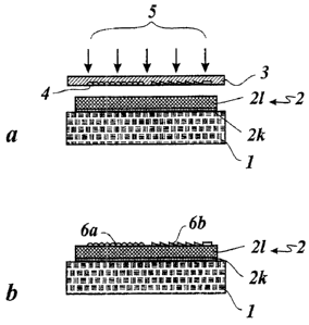
Figure la shows a carrier substrate 1 which in the illustrated
embodiment by way of example is a banknote to which there is applied a
multi-layer body 2 which is formed from an adhesive layer 2k and a
lamination layer 21 and which is applied for example as part of the transfer
layer of a hot stamping film to the carrier substrate 1. The multi-layer body
2 is In the form of a transparent multi-layer body 2 so that the multi-layer
body 2 exposes a view on to the carrier substrate 1 arranged beneath it.
Applied to the top side of the lamination layer 21 that is remote from the
carrier substrate 1, by means of an intaglio printing plate 3, is an optical
lacquer 4 which Is introduced into recesses in the intaglio printing plate 3.
CA 02593340 2007-07-10
The intaglio printing plate 3 is moved in the direction of the arrows 5 under
a high pressing force against a counter-pressure plate disposed behind the
carrier substrate, and is brought into contact with the lamination layer 21,
in
which case the optical lacquer 4 introduced into the recesses in the intaglio
printing plate 3 is released from the recesses and adheres to the top side of
the lamination layer 21. Micro-optical structures 6a and 6b are formed in
that way (see Figure lb). The optical lacquer 4 has a refractive index of
about 1.5 because the micro-optical structures 6a and 6b formed by the
lacquer adjoin air.
The micro-optical structure 6a is a micro-lens array while the micro-
optical structure 6b is an asymmetrical relief structure, for example a blaze
grating. The micro-lens array can be provided in order to optically enlarge
alphanumeric characters or an image representation printed on to the
carrier substrate. The blaze grating can be provided in order to produce an
interesting and attractive optical effect. The boundary contours of the blaze
grating can be for example in the form of a logo or an alphanumeric
character.
The intaglio printing plate 3 can be a body in plate form or a
cylindrical body or a curved plate arranged on a printing cylinder. It can be
provided that disposed on a printing cylinder or the like are further intaglio
printing plates which for example in register relationship with the micro-
optical structures 6a and 6b apply to the lamination layer 2 ink layers which
for example can form a background pattern which is partially or completely
covered by the micro-optical structures 6a and 6b.
Figures 2a and 2b now show a second embodiment by way of
example of the process according to the invention.
Figure 2a shows the multi-layer body 2 of Figure la, which is applied
to the carrier substrate 2. The multi-layer body 2 has the adhesive layer 2k
and the lamination layer 21. The intaglio printing plate 3 is now used as an
embossing tool, with which the micro-optical structures 6a and 6b are
shaped into the lamination layer 21 (see Figure 2b), under the pressing
force 5. The micro-optical structures 6a and 6b can at the same time form
a tactily perceptible security feature.
11
CA 02593340 2007-07-10
Figures 3a through 3c now show a third embodiment by way of
example of the process according to the invention.
Figure 3a shows a multi-layer body 32 applied to the carrier
substrate 1. The multi-layer body 32, like the multi-layer body 2, comprises
the adhesive layer 2k and the lamination layer 21, with an optical lacquer
layer 34 being applied to the side of the lamination layer 21, that is remote
from the adhesive layer. The optical structures 6a and 6b (see Figure 3b)
are shaped into the optical lacquer layer 34 by means of the intaglio
printing plate 3, under the pressing force 5.
Figure 3c now shows in the third step in the process the multi-layer
body 32 with a protection layer 7 applied to the surface of the lacquer layer
34. The protection layer 7 has a low refractive index, for example a
refractive index < 1.5, preferably with a refractive index %5 1. In a
preferred
embodiment the protection layer 7 is a normal cover lacquer which has a
refractive index of about 1.5 and which is applied using a screen printing
process. In that case the optical lacquer layer 34 advantageously has a
high refractive index, for example > 1.9. It can be doped to produce the
high refractive index, for example using nanoparticles. The protection layer
7 enhances the long-term stability of the micro-optical structures 6a and 6b
shaped in the lacquer layer 34 and protects them from soiling and/or wear.
Figure 4 now shows an example of use of the process according to
the invention.
On its front side a banknote 41 carries a film strip 42 which has an
OVD 420 and a latent image 421. In this embodiment the latent image 421
is formed from mutually nested blaze gratings which afford a tilting image.
A further latent image 4111$ in the form of a colored printed image and is
applied by printing to the surface of the banknote 41, which is not covered
by the film strip 42. In the embodiment illustrated in Figure 4 the latent
images 411 and 421 are arranged In mutually spaced aligned relationship.
The latent image 421 presents the letter '0' and the latent image 411
presents the letter 'K'. The latent images are only visible at a
predetermined viewing angle. From all other viewing directions they are
invisible, that is to say latent.
12
CA 02593340 2007-07-10
Beside the OVD 420 a further OVD 43 is applied to the surface of the
banknote 41 which is not covered by the film strip 42.
The banknote 41 further has a micro-lens array 44 which is arranged
over an image region 45 in register relationship. The OVDs 420 and 43 are
also arranged in register relationship with the micro-lens array 44 and are
partially covered over by the micro-lens array 44.
Arranging the micro-lens array 44, the image region 45 as well as
the OVDs 42o and 43 in register relationship is possible by the use of the
process according to the invention as described hereinbefore, under mass
production conditions, because all the elements referred to are applied to
the banknote 41 in an intaglio printing process on one installation.
Instead of the banknote it is also possible to provide any other
security document.
The banknote 41 can optionally have a window 46 which projects at
least region-wise into the region of the micro-lens array.
Figure 5 now shows a second example of use of the process
according to the invention.
A window banknote 50 which is shown as a diagrammatic view in
section comprises a carrier substrate 51 having window-like openings 51fa
and 51fb. The carrier substrate 51 can be for example a paper which is
suitable for banknotes or a plastic film. A lamination layer 52 has optically
variable elements (OVD) 52oa and 52ob which for example can be a
KINEGRAM . The KINEGRAM can be completely metallised, demetallised or
implemented with a metallisation determined by the aspect ratio of the
surface relief, it can have an HRI layer or it can be in the form of a multi-
layer, or it can be in the form of a system with color change effects, and a
(cross-linked) liquid crystal layer can be integrated into the system. The
OVD 52ob is arranged in the window opening 51fb and can therefore be
viewed both in an incident illumination mode and also in a transillumination
mode. The OVD 52oa is arranged outside the window openings 51fa and
51fb and can therefore be viewed only in an incident illumination mode
from the front side of the window banknote 50. The lamination layer 52 can
13
CA 02593340 2007-07-10
be in the form of a transparent film or in the form of a semi-transparent
film, for example a colored film.
On its underside the lamination layer 52 has an adhesive layer 53 by
means of which it is joined to the carrier substrate 51. The adhesive layer
can be a hot adhesive.
The top side of the lamination layer 52 is now printed upon with
different security elements. These involve a computer-generated hologram
549 provided with concealed information; a hologram 54h which for
example can reproduce alphanumeric characters such as a value print in a
highly effective manner; tactile features 54f which for example can provide
tactile information about the value of the banknote; and a micro-lens array
54m which in this embodiment is applied in register relationship with the
OVD 52ob arranged in the window opening 51fb. When the front side of the
window banknote 50 is viewed the micro-lens array 54m produces an
optically enlarged reproduction of the optical information stored in the OVD
52ob. In contrast, when viewing the rear side of the window banknote 50,
the micro-lens array 54m is optically not effective so that the optical
information stored in the OVD 52ob appears in its natural size. As already
described hereinbefore the holograms 54g and 54h, the tactile feature 54t
and the micro-lens array 54m are applied using intaglio printing in one
working step and are therefore arranged in strict register relationship with
each other. If therefore the micro-lens array 54m is applied in register
relationship with the OVD 52ob, then the other elements which are applied
by printing are also in register relationship with the OVD 52ob and all
further elements introduced into the lamination layer in register
relationship such as the OVD 52oa.
The computer-generated hologram 549 has pixel regions of differing
depth. The maximum pixel depth in the embodiment shown in Figure 5 is 1
i.tm, and the pixels are of a size of 1 171 X 1 gm. The concealed information
is encoded in the pixel depth which causes a change in the phase position
of the incident light. There can be provided for example between 8 and 256
different depths, that is to say, depending on the respective number of
14
CA 02593340 2007-07-10
different depths In a pixel, it is possible to store items of information of
between 8 bits and 256 bits.