Note: Descriptions are shown in the official language in which they were submitted.
CA 02593646 2007-06-22
- 1 -
CIRCUIT INTERRUPTER INCLUDING
NONVOLATILE MEMORY STORING CAUSE-OF-TRIP INFORMATION
BACKGROUND OF THE INVENTION
Field of the Invention
This invention pertains generally to circuit interrupters and, more
particularly, to circuit breakers including a trip mechanism responsive to a
plurality of
different trip conditions.
Background Information
Circuit interrupters include, for example, circuit breakers, contactors,
motor starters, motor controllers, other load controllers and receptacles
having a trip
mechanism. Circuit breakers are generally old and well known in the art.
Examples
of circuit breakers are disclosed in U.S. Patent Nos. 5,260,676; and
5,293,522.
Circuit breakers are used to protect electrical circuitry from damage
due to an overcurrent condition, such as an overload condition or a relatively
high
level short circuit or fault condition. In small circuit breakers, commonly
referred to
as miniature circuit breakers, used for residential and light commercial
applications,
such protection is typically provided by a thermal-magnetic trip device. This
trip
device includes a bimetal which is heated and bends in response to a
persistent
overcurrent condition. The bimetal, in turn, unlatches a spring powered
operating
mechanism which opens the separable contacts of the circuit breaker to
interrupt
current flow in the protected power system. An armature, which is attracted by
the
sizable magnetic forces generated by a short circuit or fault, also unlatches,
or trips,
the operating mechanism.
In many applications, the miniature circuit breaker also provides
ground fault protection. Typically, an electronic circuit detects leakage of
current to
ground and generates a ground fault trip signal. This trip signal energizes a
shunt trip
solenoid, which unlatches the operating mechanism, typically through actuation
of the
thermal-magnetic trip device. See, for example, U.S. Patent Nos. 5,260,676;
5,293,522; and 5,982,593.
Also, in many applications, miniature circuit breakers provide arc fault
protection. See, for example, U.S. Patent Nos. 5,224,006; 5,691,869; and
5,982,593.
CA 02593646 2007-06-22
- 2 -
When the circuit breaker detects a potentially hazardous fault
condition, it must open the protected power circuit as quickly as possible in
order to
interrupt the fault condition. There is a delay from the time that the circuit
breaker
electronic circuit issues a trip request to the time when the separable
contacts actually
sufficiently part and interrupt the fault condition. For example, this delay
may be in
the order of about one-half of a 60 Hz electrical cycle in a miniature circuit
breaker.
Also, when the separable contacts open, the circuit breaker electronic circuit
is
typically disconnected from its power source. There is typically sufficient
energy
storage in the circuit breaker power supply to sustain operation of the
electronic
circuit for about one-half of the 60 Hz electrical cycle after the separable
contacts
open.
Typically, faulty residential circuit breakers are returned to the
manufacturer without any information regarding the current level, the cause-of-
trip or
the count of trips. For example, known returned arc fault/ground fault circuit
breakers
provide no information to the manufacturer as to whether the circuit breaker
tripped
for arc fault or ground fault conditions, and provide no information as to the
current
level at the time of tripping.
Accordingly, there is room for improvement in circuit interrupters and
circuit breakers.
SUMMARY OF THE INVENTION
This need and others are met by embodiments of the invention, which
provide a circuit interrupter that stores in a nonvolatile memory information
regarding, for example, the current level, the cause-of-trip and the count of
trips for
use in diagnosing a fault or failure of the circuit interrupter.
In accordance with one aspect of the invention, a circuit interrupter
comprises: separable contacts; an operating mechanism structured to open and
close
the separable contacts; and a trip mechanism comprising: a sensor structured
to sense
current flowing through the separable contacts, a processor cooperating with
the
sensor to determine a plurality of different trip conditions responsive to the
sensed
current, a nonvolatile memory operatively associated with the processor, and a
trip
actuator cooperating with the processor and the operating mechanism to trip
open the
separable contacts responsive to one of the different trip conditions from the
CA 02593646 2007-06-22
- 3 -
processor, wherein the processor is structured to save in and retrieve from
the
nonvolatile memory cause-of-trip information for the different trip conditions
including the one of the different trip conditions.
The different trip conditions may include at least some of an arc fault
trip condition, a ground fault trip condition and an overload trip condition;
and the
cause-of-trip information may include one of an arc fault trip code
corresponding to
the arc fault trip condition, a ground fault trip code corresponding to the
ground fault
trip condition, and an overload trip code corresponding to the overload trip
condition.
The processor may determine a trip current corresponding to one of the
arc fault trip condition, the ground fault trip condition and the overload
trip condition;
and the processor may be further structured to save in and retrieve from the
nonvolatile memory the trip current as part of the cause-of-trip information.
The cause-of-trip information may further include a count of arc fault
trips corresponding to the arc fault trip condition, a count of ground fault
trips
corresponding to the ground fault trip condition, and a count of overload
trips
corresponding to the overload trip condition.
After power-up, the processor may be structured to increment one of a
count of arc fault trips, a count of ground fault trips and a count of
overload trips
based upon one of the arc fault trip code, the ground fault trip code and the
overload
trip code.
The different trip conditions may include a test trip condition, an arc
fault trip condition, a ground fault trip condition, a short delay trip
condition and an
overload trip condition; the processor may determine a trip corresponding to
one of
the test trip condition, the arc fault trip condition, the ground fault trip
condition, the
short delay trip condition and the overload trip condition; and the cause-of-
trip
information may further include a count of trips for each of the test trip
condition, the
arc fault trip condition, the ground fault trip condition, the short delay
trip condition
and the overload trip condition.
As another aspect of the invention, a circuit breaker comprises:
separable contacts; an operating mechanism structured to open and close the
separable
contacts; and a trip mechanism comprising: a first sensor structured to sense
current
flowing through the separable contacts, a second sensor structured to sense a
voltage
CA 02593646 2007-06-22
- 4 -
,
operatively associated with the separable contacts, a processor cooperating
with the
first sensor to determine a plurality of different trip conditions responsive
to the
sensed current, a nonvolatile memory operatively associated with the
processor, and a
trip actuator cooperating with the processor and the operating mechanism to
trip open
the separable contacts responsive to one of the different trip conditions from
the
processor, wherein the processor is structured to save in and retrieve from
the
nonvolatile memory cause-of-trip information for the different trip conditions
including the one of the different trip conditions.
The processor may include a first power supply voltage input, a second
power supply voltage input, a serial data output and a serial clock input; and
the trip
mechanism may further comprise a first terminal corresponding to the first
power
supply voltage input, a second terminal corresponding to the second power
supply
voltage input, a third terminal corresponding to the serial data output and a
fourth
terminal corresponding to the serial clock input.
The processor may be structured to input the voltage from the second
sensor and receive a periodic signal therefrom; and the processor may be
further
structured to retrieve the cause-of-trip information from the nonvolatile
memory when
the processor is powered for a predetermined time without receipt of the
periodic
signal.
BRIEF DESCRIPTION OF THE DRAWINGS
A full understanding of the invention can be gained from the following
description of the preferred embodiments when read in conjunction with the
accompanying drawings in which:
Figure 1 is a block diagram in schematic form of a circuit breaker in
accordance with an embodiment of the invention.
Figures 2A1, 2A2, 2B and 2C are flowcharts of a routine executed by
the processor of Figure 1.
Figure 3 is a block diagram of a processor for the circuit breaker of
Figure 1 in accordance with another embodiment of the invention.
CA 02593646 2007-06-22
- 5 -
DESCRIPTION OF THE PREFERRED EMBODIMENTS
The invention is described in association with a miniature, residential
circuit breaker, although the invention is applicable to a wide range of
circuit
interrupters.
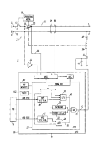
Referring to Figure 1, a circuit interrupter (e.g., without limitation, a
miniature, residential circuit breaker 1) is connected in an electric power
system 11
which has a line conductor 13 and a neutral conductor 15. The circuit breaker
1
includes a load terminal 3, a load neutral terminal 4, a line terminal 5, a
neutral
terminal 6, and separable contacts 17 which are electrically connected in
series with
the line conductor 13 between the line terminal 5 and the load terminal 3. The
separable contacts 17 are opened and closed by an operating mechanism 19. In
addition to being operated manually by a handle (not shown), the operating
mechanism 19 can also be actuated to open the separable contacts 17 by a trip
assembly 21 in response to predetermined current conditions. The trip assembly
21
includes the conventional bimetal 23 which is heated by persistent
overcurrents and
bends to actuate the operating mechanism 19 to open the separable contacts 17.
An
armature 25 in the trip assembly 21 is attracted by the large magnetic force
generated
by very high overcurrents to also actuate the operating mechanism 19 and
provide an
instantaneous trip function.
The trip assembly 21 further includes a processor (e.g., without
limitation, microcomputer ( C) 26 having a microprocessor ( P) 27) cooperating
with
the bimetal 23 to determine a plurality of different trip conditions
responsive to
current sensed from the voltage across the bimetal 23, and a nonvolatile (NV)
memory 51 operatively associated with 1.1P 27. The 1.1,P 27 of the trip
assembly 21
implements a number of different fault detection functions, such as, for
example and
without limitation, an arc fault detector (AFD) 29, a ground fault detector
(GFD) 30, a
overload detector 31 and a short delay detector 32. Alternatively, any number
of
these or other different fault detection functions may be implemented by
different
circuit structures other than or in cooperation with the IR 27.
The AFD 29 may be, for instance, of the type which detects the step
increases in current which occur each time an arc is struck, although other
types of arc
fault detectors could also be used. Suitable arc fault detectors are
disclosed, for
CA 02593646 2013-11-12
- 6 -
instance, in U.S. Patent No. 5,224,006, with a preferred type described in
U.S. Patent
No. 5,691,869. The AFD 29 senses the
current in the electrical system 11 by monitoring the voltage across the
bimetal 23 (or
other suitable current sensor (not shown)) through the lead 33 to sense an arc
fault
current condition. As described in U.S. Patent No. 5,691,869, the An) 29
includes
circuitry which generates a pulse in response to each step change in current.
The
pulse signal is integrated with the result of the integration being attenuated
over time.
When the time attenuated accumulation of the pulses reaches a selected level,
the
AFD 29 generates at its output an arc fault trip signal 38 which is active in
response to
the arc fault. In turn, the signal 38 is combined with the output trip signal
40 of the
GFD 30 and is employed to actuate the operating mechanism 19 and open the
separable contacts 17 in response to the fault.
The GFD 30 may be of the well known dormant oscillator type in
which case it utilizes a pair of sensing coils 34,35 to detect both line-to-
ground and
neutral-to-ground fault current conditions. If the AFD 29 detects an arc fault
in the
electric power system 11, the trip signal 38 is generated which, through the
IR 27,
turns on a switch such as the silicon controlled rectifier (SCR) 37 to
energize a trip
solenoid 39. When the GFD 30 detects a ground fault, it generates at its
output a
ground fault trip signal 40 which is active in response to the ground fault.
The ground
fault trip signal 40 is "ORed" with the arc fault trip signal 38 (i.e., an
"OR" function
of the outputs of the GFD 3-0,1he AFD 29, the overload detector 31 and the
short
delay detector 32), such that the combination of the various output signals,
such as
38,40, forms a fault protection trip signal 41.
Under normal operation, the trip signal 41 passes through the piP 27 to
its output 42 to turn the SCR 37 on, energize the trip solenoid 39 and,
thereby, actuate
the operating mechanism 19 to open the separable contacts 17 in response to
the arc
fault, ground fault or other trip condition. The trip solenoid 39 is, thus, a
trip actuator
cooperating with the lc' 27 and the operating mechanism 19 to trip open the
separable
contacts 17 responsive to one of the different trip conditions from the piP
27. A
resistor 43 in series with the coil of the solenoid 39 limits the coil current
and a
capacitor 44 protects the gate of the SCR 37 from voltage spikes and false
tripping
due to noise. In this manner, the arc fault condition, the ground fault
condition or
.;.t
CA 02593646 2007-06-22
- 7 -
other trip condition results in the interruption of electrical power
independent of the
others.
One or both of the AFD 29 and the GFD 30 may have a test circuit,
such as 45 and 49, respectively. These circuits may be external to or internal
to the
ill) 27, as shown. Under test operation, if the GFD 30 and/or the AFD 29 are
operating properly, then they generate the trip signals 40 and 38 when the
corresponding one of the test circuits 49,45, respectively, is enabled. The
test circuit
49, when enabled by the test button 9, generates a test signal to the GFD 30
to
simulate a ground fault current condition by mimicking ground faults in the
electrical
system 11 and, thereby, testing operation of the GFD 30. The test circuit 45
may also
provide signals to the AFD 29 to simulate an arc fault current condition by
mimicking
arc faults in the electrical system 11 and, thereby, testing operation of the
AFD 29.
The test circuit 45 preferably includes a low frequency relaxation oscillator
and a
coupling circuit for coupling a pulse signal generated by the relaxation
oscillator to
the AFD 29.
The bimetal 23 forms a first sensor structured to sense current flowing
through the separable contacts 17. As shown in Figure 1, the trip assembly 21
may
also include a second sensor 50 structured to sense a voltage operatively
associated
with the separable contacts 17. In this example, the load side of the
separable
contacts 17 is at a common ground reference and the line-to-neutral voltage
is, thus,
sensed from the neutral conductor 15. As will be described, below, in
connection
with Figures 2A1, 2A2, 2B and 2C, the 11C 29 includes the suitable NV memory
51,
and the .13 27 is structured to save in and retrieve from such NV memory
cause-of-
trip information for the different trip conditions.
Figures 2A1, 2A2, 2B and 2C are flowcharts of a routine 100 executed
by the vtP 27 of Figure 1. After power-up, at 102, the [tP 27 resets and
starts a
timer 103 (Figure 1), at 104. Next, at 106, it is determined if a suitable
time (e.g.,
without limitation, one second) has elapsed since the timer 103 was started.
If not,
then, at 108, it is determined whether a periodic voltage zero-crossing signal
has
occurred as detected through sensor 50. The 13 27 inputs the voltage from the
sensor
50 and normally receives the periodic signal (e.g., without limitation, a zero-
crossing
signal of the line-to-neutral voltage) therefrom. If not, then step 106 is
repeated. On
CA 02593646 2007-06-22
- 8 -
the other hand, if a periodic voltage zero-crossing signal has occurred, then
normal
start-up processing begins at 144 of Figure 2B.
If, at 106, a suitable time has elapsed since the timer 103 was started,
then, at 110, a byte pointer and a bit pointer are both set to one. Even steps
110-142
provide a mechanism to read-out diagnostic information from the NV memory 51
when the circuit breaker 1 is powered in the manner as will be described,
below, in
connection with Figure 3, and is not powered through a power supply (not
shown) by
the line-to-neutral voltage from the line terminal 5 and the neutral terminal
6. As
such, the IR 27 retrieves the cause-of-trip information from the NV memory 51
when
it determines that it is powered for a predetermined time without receipt of
the
periodic signal from the line-to-neutral voltage. Then, the [LI) 27 outputs
the cause-of-
trip information from the NV memory 51 on the COMM serial data output 254
(Figure 3) responsive to the COMM serial clock input 256 (Figure 3).
Table 1, below, shows an example structure of a portion of the NV
memory 51. Of interest, one of the single stored bytes contains a cause-of-
trip code in
the upper nibble thereof that records the type of trip condition, while the
lower nibble
thereof records the peak current (divided by 20) at the time of trip.
Alternatively, the
meaning of the information stored in the lower nibble may differ based upon
the
specific trip or test condition as indicated by the upper nibble. As is
discussed, below,
the single byte is stored in the first cause-of-trip location of Table 1 when
the circuit
breaker 1 trips. Later, when the circuit breaker 1 powers on, the circuit
breaker P 27
processes the cause-of-trip information into a relatively more detailed trip
record.
The various cause-of-trip information further includes a count of arc fault
trips
corresponding to arc fault trip conditions, a count of ground fault trips
corresponding
to ground fault trip conditions, a count of short delay trips corresponding to
short
delay trip conditions, and a count of overload trips corresponding to overload
trip
conditions.
CA 02593646 2007-06-22
- 9 -
Table 1
Firmware code version (byte 1)
Firmware code version (byte 2)
Date code (byte 1)
Date code (byte 2)
Date code (byte 3)
Failure code
Cause-of-trip code (peak current)/20
Last Cause-of-trip code (peak current)/20
GF counter (byte 1)
GF counter (byte 2)
Short delay counter (byte 1)
Short delay counter (byte 2)
AF counter (byte 1)
AF counter (byte 2)
Overload counter (byte 1)
Overload counter (byte 2)
Test button counter (byte 1)
Test button counter (byte 2)
Test button counter (byte 20)
The IP 27 is operatively associated with a firmware code version
level, which is stored in two bytes, and a manufacture date code for the trip
assembly
21, which is stored in three bytes of the NV memory 51. Alternatively, or in
addition,
the NV memory 51 may include analog offset information (not shown) for the
analog-
to-digital converter (ADC) of the RC 26. The NV memory 51 also saves in two
bytes
different values (e.g., 255 x 2 = 510 possible maximum trips) for the count of
trips
corresponding to the ground fault trip condition, the short delay trip
condition, the arc
fault trip condition and the overload trip condition. The NV memory 51 further
saves
in twenty bytes the value (e.g., 255 x 20 = 5100 possible maximum trips) for
the
CA 02593646 2007-06-22
- 10 -
count of test trip conditions. The NV memory 51 may also include a failure
code (one
byte) for non-recoverable hardware faults, which are distinct from system
fault
conditions like, for example, ground faults or arc faults. Additional
information, such
as the count of ON/OFF cycles (not shown) and the "line voltage" (not shown)
may
also be stored, as needed, in the NV memory 51.
Next, at 112 of Figure 2A1, the trip signal 41 is output by the 111) 27.
This step, which is periodically executed when the COMM serial clock input 256
is
low, periodically actuates the trip solenoid 39 when the uP 27 is powered for
a
predetermined time without receipt of the periodic line-to-neutral voltage.
This is
either a safety precaution in the event that the line terminal 5 might be
energized, or,
alternatively, provides a "heartbeat" signal to indicate that the 1.IP 27 is
running. At
114, it is determined whether a low-to-high transition occurred on the COMM
serial
clock input 256 (Figure 3). If not, then step 112 is repeated such that the
trip signal
41 is periodically output. Otherwise, if the low-to-high transition occurred,
then, at
116, the tC timer 103 is reset and started.
Next, at 118, the bit designated by the combination "byte pointer : bit
pointer" of step 110 is output on the COMM serial data output 254 (Figure 3).
Next,
at 120, it is determined whether a high-to-low transition occurred on the COMM
serial clock input 256 (Figure 3). If not, then, at 122, it is determined if a
suitable
time (e.g., without limitation, one second) elapsed since the timer 103 was
reset. If
not, then step 120 is repeated. If so, then step 110 is repeated since the
diagnostic
information from the NV memory 51 was improperly read-out. As such, the pi' 27
repeats retrieval of the cause-of-trip information from the NV memory 51 and
outputs
the same on the COMM serial data output 254 responsive to the COMM serial
clock
input 256 being static for a predetermined time.
Otherwise, in response to the high-to-low transition on the COMM
serial clock input 256, at step 124, the [IC timer 103 is reset and started.
Next, at 126,
the bit pointer is incremented. At 128, if the bit pointer is greater than 8,
then, at 130,
the bit pointer is set to 1 and, at 132, the byte pointer is incremented.
Otherwise, at
128, if the bit pointer is not greater than 8, or after 132, then, at 134, it
is determined if
the byte pointer is greater than 28. If so, then a "failure code" in the NV
memory 51
is cleared before entering an endless loop at 142. On the other hand, if the
byte
CA 02593646 2007-06-22
- 11 -
pointer is not greater than 28, at 134, then, at 136, it is determined whether
a low-to-
high transition occurred on the COMM serial clock input 256 (Figure 3). If so,
then
step 116 is repeated. Otherwise, at 138, it is determined if a suitable time
(e.g.,
without limitation, one second) elapsed since the timer 103 was started. If
not, then
step 136 is repeated. If so, then step 110 is repeated.
At 144 of Figure 2B, it is determined if the cause-of-trip from the NV
memory 51 is zero. If so, then normal circuit breaker processing begins at
step 192 of
Figure 2C. Otherwise, the circuit breaker 1 was previously tripped, and after
power-
up, even steps 146-186 of Figures 2B-2C determine the type of the trip
condition and
increment the corresponding counter in NV memory 51 for the count of arc fault
trips,
the count of ground fault trips, the count of overload trips and the count of
short delay
trips based upon one of the arc fault trip code, the ground fault trip code,
the overload
trip code and the short delay trip code in NV memory 51. If the upper nibble
of the
cause-of-trip byte is non-zero at power-up, then an NV byte associated with
that
"cause-of-trip" is incremented (unless all associated bytes are saturated),
the "cause-
of-trip" byte is written into the "last cause-of-trip" NV byte (if it is a
protective trip)
and the cause-of-trip byte is cleared to zero. However, a test button trip
counter is
incremented (at 204 of Figure 2C) before a trip is initiated. Each "cause-of-
trip" has
two or more NV bytes for recording the count of those trips. Each byte
saturates at
255 and ceases to be updated.
At 146, the upper nibble of the cause-of-trip byte is extracted and
includes one of the following different cause-of-trip codes: (0) no trip
cause; (1)
ground fault trip; (2) short delay trip; (3) arc fault trip; (4) overload
trip; and (5-15)
any other suitable trip/condition code. At 148, if the code is 1 for a ground
fault trip,
then even steps 150-156 update the corresponding GF counter. At 150, if the
first
byte of the GF counter is less than 255, then the first byte of the GF counter
is
incremented at 152. Otherwise, at 154, if the second byte of the GF counter is
less
than 255, then the second byte of the GF counter is incremented at 156. After
either
152 or 156, execution resumes at 188 of Figure 2C.
At 158, if the-code is 2 for a short delay (SD) trip, then even steps 160-
166 update the corresponding SD counter. At 160, if the first byte of the SD
counter
is less than 255, then the first byte of the SD counter is incremented at 162.
CA 02593646 2007-06-22
- 12 -
Otherwise, at 164, if the second byte of the SD counter is less than 255, then
the
second byte of the SD counter is incremented at 166. After either 162 or 166,
execution resumes at 188 of Figure 2C.
At 168, if the code is 3 for an arc fault (AF) trip, then even steps 170-
176 update the corresponding-AF counter. At 170, if the first byte of the AF
counter
is less than 255, then the first byte of the AF counter is incremented at 172.
Otherwise, at 174, if the second byte of the AF counter is less than 255, then
the
second byte of the AF counter is incremented at 176. After either 172 or 176,
execution resumes at 188 of Figure 2C.
At 178 of Figure 2C, if the code is 4 for an overload trip, then even
steps 180-186 update the corresponding overload counter. At 180, if the first
byte of
the overload counter is less than 255, then the first byte of the overload
counter is
incremented at 182. Otherwise, at 184, if the second byte of the overload
counter is
less than 255, then the second byte of the overload counter is incremented at
186.
After either 182 or 186, execution resumes at 188 where the NV last cause-of-
trip is
set equal to the cause-of-trip. Then, at 190, the cause-of-trip is set equal
to zero.
At 192, the p,P 27 reads the various current values as sensed by the
bimetal 23 and the sensing coils 34,35 (Figure 1). Steps 193, 194 and 196
respectively provide an overload (OL)/short delay (SD) routine, a GFD routine
and an
AFD routine. During each of these routines, the P 27 determines if a trip
current
corresponds to one of the overload or short delay trip condition, the ground
fault trip
condition and the arc fault trip condition, and, if so, saves in and retrieves
from the
NV memory 51 the trip current as part of the cause-of-trip information.
Next, at 198, it is determined if the test pushbutton 9 (Figure 1) is
depressed. If so, then even steps 200-208 update the corresponding test
counter in
NV memory 51. At 200, an integer n is set to 1. At 202, it is determined if
the test
byte counter (byte n) is less than 255. If so, then at 204, the corresponding
test byte
(byte n) counter is incremented after which execution resumes at 210. Here,
the count
of trips corresponding to the test trip condition is incremented before the
13 27
actuates the trip solenoid 39.
Otherwise, at 202, if the corresponding test byte (byte n) counter is not
less than 255, then at 206, it is determined if the integer n is less than 20.
If not, then
CA 02593646 2007-06-22
- 13 -
execution resumes at 210. Otherwise, if the integer n is less than 20, then
the integer
n is incremented, at 208, and execution resumes at 202.
Step 210 processes the test pushbutton 9, which may provide one or
two inputs for the corresponding ground fault test circuit 49 and the arc
fault test
circuit 45. In turn, the pP 27 actuates the trip solenoid 39 to trip open the
separable
contacts 17 responsive to actuation of the test button 9.
Upon tripping in any of steps 193, 194, 196, 210, protective "cause-of-
trip" or test button trip information is saved in the upper nibble of the
cause-of-trip
byte in NV memory 51 (Table 1) and the peak current at tripping (divided by
20) is
saved in the lower nibble of that cause-of-trip byte. When multiplied by 20 A,
the
lower nibble saturates at 15 counts or 300 A. The upper nibble of the cause-of-
trip
byte includes one of the following different cause-of-trip codes: (0) no trip
cause; (1)
ground fault trip; (2) short delay trip (e.g., without limitation, sustained
high current >
250 A); (3) arc fault trip; (4) overload trip; and (5-15) any other suitable
trip/condition=
code.
After the circuit breaker 1 issues a trip request, but before the circuit
breaker electronic trip assembly 21 loses power, there is some opportunity to
store
information about the trip cause in NV memory 51. For example, the worst case
time
to store information in NV memory 51 may be on the order of about 10 mS. In
this
example, there is sufficient tithe to store only minimal information. This
example
stores a single byte of cause-of-trip information, although any suitable count
of bytes
may be stored as time permits.
Figure 3 shows RC 26' which may be the same as or similar to the p,C
26 of Figure 1. The pC 26' includes a first power supply voltage input (VDD)
250, a
second power supply voltage input (Vss) 252, a COMM serial data output 254 and
a
COMM serial clock input 256. The trip assembly 21 (Figure 1) includes a first
terminal 258 corresponding to the first power supply voltage input 250, a
second
terminal 260 corresponding to the second power supply voltage input 252, a
third
terminal 262 corresponding to the COMM serial data output 254 and a fourth
terminal
264 corresponding to the COMM serial clock input 256. The terminals
258,260,262,264 may be, for example, printed circuit board pads (not shown)
that can
be electrically engaged by a suitable diagnostic circuit (not shown) that
provides
CA 02593646 2007-06-22
- 14 -
power to the power supply voltage inputs 250,252, a suitable clock to the COMM
serial clock input 256 and receives the data from the COMM serial data output
254.
Under normal operation of the circuit breaker 1 (Figure 1), the uP 27
receives a periodic line-to-neutral voltage zero-crossing signal from sensor
50 during
powered operation. As was discussed above in connection with Figures 2A1-2A2,
if
the circuit breaker 1 is powered for about 1 second without the periodic line-
to-neutral
voltage zero-crossing signal, then the RP 27 assumes it is in an interrogation
mode,
periodically sends the trip signal 41 to the trip solenoid 39 and monitors the
COMM
serial clock input 256. When a low-to-high "clock" transition is detected, NV
byte
information is serially downloaded, least significant bit first, at a maximum
rate of
about 1000 bits per second. If the clock is static high or low for one second,
then the
NV byte pointer returns to the first NV byte. If communication of all NV bytes
is
successful, then the cause of failure byte is cleared and writes to NV memory
51 are
inhibited (at step 142 of Figure 2A2) until a power down reset occurs.
The example miniature residential circuit breaker 1 includes a
microprocessor-controlled protection circuit as part of the C 26. The RP 27
generates a trip, for example, in response to arc fault conditions, ground
fault
conditions, overload and/or short delay trip conditions. The cause-of-trip
data and trip
current level are stored at the time of trip in NV memory 51. Furthermore,
four
terminals 258,260,262,264 (e.g., printed circuit board pad connections) are
provided
such that when the circuit breaker 1 is returned to the manufacturer, the 13
27 can be
interrogated to extract meaningful trip information.
While specific embodiments of the invention have been described in --
detail, it will be appreciated by those skilled in the art that various
modifications and
alternatives to those details could be developed in light of the overall
teachings of the
disclosure. Accordingly, the particular arrangements disclosed are meant to be
illustrative only and not limiting as to the scope of the invention which is
to be given
the full breadth of the claims appended and any and all equivalents thereof
CA 02593646 2014-06-04
- 15 -
REFERENCE NUMERICAL LIST
circuit interrupter (e.g., without limitation, a miniature, residential
circuit breaker)
3 load terminal
4 load neutral terminal
line terminal
6 neutral terminal
11 electric power system
13 line conductor
neutral conductor
17 separable contacts
19 operating mechanism
21 trip assembly
23 conventional bimetal
armature
26 processor (e.g., without limitation, microcomputer (vC))
26' processor
27 microprocessor (.1P)
29 arc fault detector (AFD)
ground fault detector (GFD)
31 overload detector
32 short delay detector
33 lead
34 sensing coil
sensing coil
37 silicon controlled rectifier (SCR)
38 arc fault trip signal
39 trip solenoid
ground fault trip signal
41 fault protection trip signal
42 output
43 resistor
44 capacitor
test circuit
49 test circuit
second sensor
51 nonvolatile (NV) memory
100 routine
102 step
103 timer
104 step
106 step
108 step
110 step
112 step
114 step
116 step
CA 02593646 2014-06-04
- 16 -
118 step
120 step
122 step
124 step
126 step
128 step
130 step
132 step
134 step
136 step
138 step
140 step
142 step
144 step
146 step
148 step
150 step
152 step
154 step
156 step
158 step
160 step
172 step
174 step
176 step
178 step
180 step
182 step
184 step
186 step
188 step
190 step
192 step
193 step
194 step
196 step
198 step
200 step
202 step
204 step
206 step
208 step
210 step
250 first power supply voltage input (VDD)
252 second power supply voltage input (Vss)
254 COMM serial data output
256 COMM serial clock input
CA 02593646 2014-06-04
- 17 -
258 first terminal-
260 second terminal
262 third terminal
264 fourth terminal