Note: Descriptions are shown in the official language in which they were submitted.
CA 02593734 2007-06-22
WO 2006/071477 PCT/US2005/044204
RADIO FREQUENCY IDENTIFICATION DEVICE WITH VISUAL INDICATOR
BACKGROUND OF THE INVENTION
TECHNICAL FIELD OF THE INVENTION
[0001] The invention relates to radio frequency identification (RFID) devices.
DESCRIPTION OF THE RELATED ART
[0002] Radio frequency identification (RFID) tags and labels (collectively
referred
to herein as "devices") are widely used to associate an object with an
identification
code. RFID devices generally have a combination of antennas and analog and/or
digital electronics, which may include for example communications electronics,
data
memory, and control logic. For example, RFID tags are used in conjunction with
security-locks in cars, for access control to buildings, and for tracking
inventory and
parcels. Some examples of RFID tags and labels appear in U.S. Patent Nos.
6,107,920, 6,206,292, and 6,262,692, all of which are hereby incorporated by
reference in their entireties.
[0003] As noted above, RFID devices are generally categorized as labels or
tags.
RFID labels are RFID devices that are adhesively or otherwise have a surface
that is
attached directly to objects. RFID tags, in contrast, are secured to objects
by other
means, for example by use of a plastic fastener, string or other fastening
means.
Nevertheless, RFID devices are referred to herein somewhat interchangeably as
"tags" or "labels."
[0004] In activating, reading, and/or detecting RFID devices, radio frequency
(RF)
fields are generally sent over a relatively long range, that is, over
intervening free
space. Thus detection of devices is accomplished over a significantly-sized
region,
and spatial discrimination in reading and detection of devices may be
difficult.
[0005] One concern that has been raised regarding RFID devices is that their
ability to be read over relatively long distances may implicate privacy
concerns for
people having objects with RFID devices attached thereto or otherwise coupled
thereto. It will be appreciated that concerns about possible tracking or other
privacy-
related issues may inhibit some users from employing RFID devices.
Accordingly, it
1
CA 02593734 2007-06-22
WO 2006/071477 PCT/US2005/044204
will be appreciated that it would be desirable for RFID devices to avoid the
above
problems.
SUMMARY OF THE INVENTION
[0006] According to an aspect of the invention, an RFID device includes a
display
that selectively shows one or more visual indicators. Display of the one or
more
visual indicators may be actuated based on an operating state of the RFID
device.
[0007] According to another aspect of the invention an RFID device includes an
electrochromic display that is operatively coupled to a chip of the device.
[0008] According to still another aspect of the invention, an RFID device
includes a
display for displaying a visual indication of the disabling of operation of
the RFID
device.
[0009] According to a further aspect of the invention, an RFID device includes
a
display for displaying a visual indicator that is readable only using light
outside of the
wavelength range normally viewable by humans (i.e., ultraviolet light and/or
infrared
light).
[0010] According to a still further aspect of the invention, an RFID device
includes:
a chip; an antenna operatively coupled to the chip; and a display operatively
coupled
to the chip. The antenna is configured for receiving energy to power the chip.
The
antenna is configured to receive information signals to be passed on to the
chip.
The display includes a visual indicator that provides a visual indication of
an
operative state of the device.
[0011] According to another aspect of the invention, an RFID device includes:
a
chip; an antenna operatively coupled to the chip; and a display operatively
coupled
to the chip. The antenna is configured to receive information signals to be
passed
on to the chip. The display includes a visual indicator that provides a visual
indication that normal operation of the device is disabled.
[0012] According to yet another aspect of the invention, a method of using a
radio
frequency identification (RFID) device includes the steps of: disabling normal
operation of the device, thereby placing the device in a disabled state; and
displaying
a visual indication on a display of the device, wherein the visual indication
indicates
the disabled state.
2
CA 02593734 2007-06-22
WO 2006/071477 PCT/US2005/044204
[0013] To the accomplishment of the foregoing and related ends, the invention
comprises the features hereinafter fully described and particularly pointed
out in the
claims. The following description and the annexed drawings set forth in detail
certain
illustrative embodiments of the invention. These embodiments are indicative,
however, of but a few of the various ways in which the principles of the
invention
may be empioyed. Other objects, advantages and novel features of the invention
will become apparent from the following detailed description of the invention
when
considered in conjunction with the drawings.
BRIEF DESCRIPTION OF THE DRAWINGS
[0014] In the annexed drawings, which are not necessarily to scale:
[0015] Fig. 1 is an oblique view of a RFID device in accordance with the
present
invention;
[0016] Fig. 2 is a block diagram of one possible configuration of the RFID
device
of Fig. 1;
[0017] Fig. 3 is a schematic diagram showing interaction of an RFID
reader/detector, and the RFID device of Fig. 1;
[0018] Fig. 4A is a schematic illustration of an alternate configuration of
the RFID
device of Fig. 1;
[0019] Fig. 4B is a schematic illustration of a voltage multiplier that may be
part of
an RFID device in accordance with the present invention;
[0020] Fig. 4C is a schematic illustration of a voltage converter that may be
part of
an RFID device in accordance with the present invention;
[0021] Fig. 4D is another possible configuration of the RFID device of Fig. 1;
[0022] Fig. 5 is a high-level flowchart illustrating some steps in the
operation of the
display of the RFID device of Fig. 1;
[0023] Fig. 6 schematically illustrates an electrochromic display for possible
use
with the RFID device of Fig. 1;
[0024] Fig. 7 schematically illustrates a liquid crystal display for possible
use with
the RFID device of Fig. 1;
[0025] Fig. 8 is a plan view of an RFID device, in accordance with the present
invention, that utilizes a thermochromic display;
3
CA 02593734 2007-06-22
WO 2006/071477 PCT/US2005/044204
[0026] Fig. 9 is a schematic diagram illustrating configuration of a
chemically-
reactive-material display, for possible use with the RFID device of Fig. 1;
[0027] Figs. 10 and 11 illustrate two possible visual indicators that may be
displayed in use of the RFID device of Fig. 1;
[0028] Figs. 12 and 13 respectively illustrate obscured and revealed
information
that is part of a display that is usable with the RFID device of Fig. 1; and
[0029] Fig. 14 schematically illustrates another type of RFID device, with a
display
that integrated with an antenna and a chip, in accordance with the present
invention.
DETAILED DESCRIPTION
[0030] An RFID device includes a chip, an antenna operatively coupled to the
chip,
and a visual indicator operatively coupled to the chip. The visual indicator
provides a
visual indication of an operative state of the device. The visual indication
may be
human readable and/or machine readable, and may provide visual indication that
is
dependent on a change in an operative state of the device. The operative state
that
triggers the visual indication may include a state in which the chip has
temporarily or
permanently been rendered inoperative or disabled, that is, in which the chip
no
longer responds to, or otherwise interacts with, ordinary incoming RF signals
such as
from a device reader. The visual indicator may be included in a display that
functions by any of a variety of suitable mechanisms, such as by use of
electrochromic materials, thermochromic materials, liquid crystals, or
chemically-
reactive materials. The visual indication may include any of a wide variety of
human-
readable or machine-readable indications, for example, including words,
symbois,
and/or colors, and/or by hiding and/or revealing underlying human-readable or
machine-readable indicia. The display that includes the visual indicator may
have a
single changeable element, or may have multiple elements. Displays with
multiple
elements may be configured to show different combinations of elements to
provide
visual indications of different operative states of the RFID device. The
device with
the visual indicator may be used to communicate a wide variety of different
information on operative states, for a wide variety of different purposes. One
possible use for the RFID device is to provide a visual indication when the
device is
rendered permanently inoperative following the receipt by the device of a
signal
4
CA 02593734 2007-06-22
WO 2006/071477 PCT/US2005/044204
indicating that the device is to disable itself from further operation. Such a
visual
indication of device inoperabiiity may aid in allaying privacy-based concerns
regarding RFID devices.
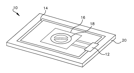
[0031] Referring to Fig. 1, an RFID device 10 includes a chip 12, an antenna
14
coupled to the chip 12, and a display 16 coupled to the chip 12. The display
16
includes a visual indicator 18 for providing a human-readable and/or machine-
readable visual indication of an operative state of the RFID device 10. The
visual
indicator 18 may indicate an operative state of the chip 12. All of the
components
12-18 of the RFID device 10 may be mounted on a suitable substrate 20.
[0032] A "transponder chip" or "chip" is defined as a device for providing
suitable
interaction, through an antenna, for communication with an external device,
such as
a reader. A chip may include any of a variety of suitable electrical
components, such
as resistors, capacitors, inductors, batteries, memory devices, and
processors. It will
be appreciated that a large variety of transponder chips for RFID devices are
widely
known. The term "transponder chip" is intended to encompass the broad range of
such devices, which may vary widely in complexity and functionality.
[0033] The antenna 14 may be any of a variety of suitable types of antennas
for
RFID devices. Examples of suitable types of antennas include dipole antennas,
loop
antennas, slot antennas, coil antennas, and hybrid antennas combining
structures
and characteristics of various antenna types.
[0034] The chip 12 and the antenna 14 may interact with a communication
device,
such as an RFID device reader or detector, in a variety of suitable ways. The
RFID
device 10 may be a fully passive device, in which the antenna 14 receives
signals
which, when rectified, provide power for the chip 12, and, if required provide
commands from the reader to the chip in the form of amplitude modulation of
the
signal. To send a signal from the RFID device to the reader, the device
modulates
its input impedance with a data-carrying signal. For low frequency tags, those
operating at typically 125kHz and 13.56MHz, the effect of this modulation is
best
described as an increase in the load presented to the reader transmitter, for
high
frequency signals, such as those in the band 902 - 928MHz, it is usually
described
as a form of reflection or backscatter modulation.
CA 02593734 2007-06-22
WO 2006/071477 PCT/US2005/044204
[0035] Alternatively, the RFID device 10 may be a semi-passive RFID device. As
with a fully passive RFID device, a semi-passive RFID device does not generate
its
own radio signals. However, unlike the fully passive device, in the semi-
passive
device the logic functions of the chip 12, and the communication functions of
the chip
12, are powered by a battery or other energy storage device. Communication
with a
semi-passive device is similar to communication with a fully passive device,
in that in
both devices communication from the device occurs by reflection of an incident
signal back to a device reader or detector.
[0036] Another alternative for the RFID device 10 is an active RFID device. An
active device contains its own power source, such as a battery, for providing
power
to the chip 12, and for transmitting signals from the chip 12, via the antenna
14.
[0037] The communication by RF signals of the RFID device 10 with external
devices is referred to herein as normal operation of the RFID device 10. This
normal
operation may be accomplished by reflecting of signals (for passive and semi-
passive devices) or by the transmitting of signals (for active devices). An
RFID
device that is rendered by internal mechanisms temporarily or permanently
unable to
send signals (by reflecting or transmission) is referred to herein as being
disabled.
[0038] The display 16 may be any of a variety of suitable types of displays.
Examples of such displays include electrochromic displays, thermochromic
displays,
liquid crystal displays (LCDs), and displays containing chemically-reactive
materials.
At least some of these types of displays are discussed in greater detail
below. The
display 16 may have its own power source, such as from a battery or a
capacitor.
Alternatively, or in addition, the display 16 may utilize the same active or
passive
power source used to power the chip 12.
[0039] The visual indicator 18 may include any of a wide variety of types of
visual
elements that are readable or otherwise detectable by human vision and/or
machine
vision. The visual indicator may include a plurality of separately or
simultaneously
actuatable elements, or may alternatively be a single element. The visual
indicator
18 provided may include display of one or more symbols, such as the display of
letters or words. Alternatively, or in addition, the visual indicator 18 may
include
graphic elements, such as stylized pictures. The visual indicator 18 may
include a
change of color, either alone or in addition to the display of other types of
visual
6
CA 02593734 2007-06-22
WO 2006/071477 PCT/US2005/044204
elements. The visual indicator 18 may also include a change in emissivity of a
material, for example, revealing or obscuring visible indicia, such as printed
matter,
that are underneath the display 16. Such indicia, for example, including bar
code
elements, may be printed on the substrate 20. It will be appreciated that
color
change in the visual indicator 18 may be used to obscure or reveal underlying
material, for example, visual elements printed in a similar color. The visual
indicator
18 may involve visual material which may be viewed under ordinary human-
visible
light. Alternatively or in addition, the visual indicator 18 may involve
material that is
visually-readable only in other sorts of light, such as infrared light or
ultraviolet light.
A further possibility for the visual indicator 18 is an indicator such as a
bar code that
is visually detectable by humans, but is only meaningfully deciphered (read)
by or
with the assistance of machines or devices.
[0040] The RFID device 10 may include a wide variety of other layers and/or
components. For example, the RFID device 10 may be a label that includes an
adhesive layer with a peelable cover layer. As another example, the RFID
device 10
may include protective layers for protecting the operative components of the
device,
and/or may include a printable layer or region, for example, for including a
bar code
or other information.
[0041] Fig. 2 shows a block diagram of one possible configuration of a fully
passive
version of the RFID device 10. Fig. 3 schematically illustrates interaction
between
an RFID device reader or detector 22, and the RFID device 10 of Fig. 2.
Antenna
elements 30 and 32 of the device 10 receive signals 34 and 36 sent by the
device
reader 22. The signals sent by the device reader 22 include an unmodulated
continuous-wave RF power signal 34, and an amplitude modulated RF instruction
signal 36. The unmodulated power signal 34 provides power to the RFID device
10,
while the instruction signal 36 provides commands to the chip 12 of the device
10.
The signals 34 and 36 may be sequentially emitted by the reader 22, in order
to
power the device 10, and to interrogate or command the RFID device 10.
Alternatively, in the situation where a reduced amplitude modulation depth
data
signal is used, the device 10 may receive power and commands simultaneously.
[0042] Both of the signal types 34 and 36 are received by the antenna elements
30
and 32 of the device 10. The element 32 acts as a power ground for the device
10.
7
CA 02593734 2007-06-22
WO 2006/071477 PCT/US2005/044204
Signals from the antenna element 30 pass through a rectifier 40, and into a
chip logic
block 41. Specifically, the incoming signal from the rectifier 40 enters the
chip logic
block 41 through a power port 42 and a data in port 44. The data out port 48
of the
logic block 41 may be coupled to a modulation transistor 50 for changing
impedance
of the device 10. The modulation transistor 50 is coupled to both of the
antenna
elements 30 and 32. The incoming power signal 34 provides power for operating
the
chip logic block 41. The logic block 41 acts upon commands that are received
by the
incoming instruction signal 36. These instructions may involve having the
logic block
41 modify a register in a memory location 56. Instructions may also involve
sending
a signal through the data out port 48 to modulate impedance through the
modulation
transistor 50. This change in impedance may be detected by the reader/detector
22
in its effect on the unmodulated power signal 34. The antenna element 32,
which
functions as a power ground, is also coupled to a ground port 60 of the logic
block
41.
[0043] The logic block 41 may be configured such that when a predetermined
value
is placed in a memory location 56, a switch 62 is tripped to provide high
voltage
through a power output port 64 and to the display 16. (A predetermined input
signal
may be used to put the value in the memory location 56.) The "high voltage"
supplied through the power output port may be a rectified supply voltage, such
as at
around 1-2 volts. The display 16 is also coupled to the ground port 60.
Providing
high voltage through the power output port 64 causes a change in a visual
indicator
18 of the display. Thus, the device 10 is configured such that writing of a
predetermined value to the memory location 56 also results in display of the
visual
indicator 18.
[0044] The signal sent to the RFID device 10 to trigger display of the visual
indicator 18 may be a "kill" or "self-destruct" signal that disables operation
of the
logic 41 of the chip 12. Examples of such signals may be found in Technical
Report:
13.56 MHz ISM Band Class 1 Radio Frequency Identification Tag Interface
Specification: Candidate Recommendation, Version 1Ø0 (describing a Destroy
command); Draft Protocol Specification For a 900 MHZ Class 0 Radio Frequency
Identification Tag (describing a Kill function); and Technical Report: 860 MHz-
930MHz Class I Radio Frequency Identification Tag Radio Frequency & Logical
8
CA 02593734 2007-06-22
WO 2006/071477 PCT/US2005/044204
Communication Interface Specification Candidate Recommendation, Version 1Ø1.
All of these reports are published by the Auto-ID Center of the Massachusetts
Institute of Technology, all are available on line at www.epcglobalinc.org,
and all are
incorporate herein by reference.
[0045] The above-described de-activation of the chip 12 may be a reversible or
irreversible operation. Further, the device 10 may be configured so that only
some
of kill or disable signals trigger activation of the display 16. For example,
the device
may be configured so that a password, key, or other specific type of kill
command
triggers activation of the display 16.
[0046] Fig. 4A illustrates one possible alternate configuration for providing
switchable power to the display 16, through a pair of input/output ports 65
and 66
that are part of the logic block 41. A pair of field effect transistors 67 and
68 are
coupled to a system supply voltage Vdd and a system ground voltage Vss. An
internal driver 69 of the logic block 41 provides signals X and Y to the field
effect
transistors 67 and 68 to direct the desired voltage to the ports 65 and 66.
The
signals X and Y may configure the field effect transistors 67 and 68 to
provide the
same voltage, either Vdd or Vss, to both of the ports 65 and 66, providing no
voltage
difference across the display 16. The signals X and Y may also be used to
provide a
voltage difference across the ports 65 and 66 in either direction (and thus
across the
display 16 as well), with the supply voltage Vdd supplied to either port, and
with
ground voltage supplied to the other port. Thus the display 16 may be driven
in
either direction.
[0047] Various forms of voltage converters or voltage multipliers may also be
used
as part of the device 10, as illustrated in Figs. 4B and 4C, to increase the
supply
voltage of the device 10. The voltage multiplier 70 shown in Fig. 4B shows a
field
effect transistor 72 coupled to a supply voltage Vdd and a ground voltage Vss.
A
pair of diodes 74 and 75 and a pair of capacitors 76 and 77 are used to
increase the
output voltage 78 of the voltage multiplier. Depending upon the input signal X
to the
field effect transistor 72, the output voltage 78 may be up to two times the
supply
voltage Vdd. The output voltage 78 may be used to drive the display 16 (Fig.
4A), or
may be fed to further voltage multipliers.
9
CA 02593734 2007-06-22
WO 2006/071477 PCT/US2005/044204
[0048] Fig. 4C illustrates a voltage converter 80 that includes an inductor 82
coupled to a supply voltage Vdd. A transistor 83 is coupled to output from the
inductor 82 and to a ground voltage Vss. A diode 84 and an output capacitor 86
also
make up part of the voltage converter 80. The transistor 83 sequentially
shorts the
inductor 82 across the supply voltage Vdd and the ground voltage Vss. As the
current through the inductor 82 changes, it generates a voltage proportional
to the
rate of change of the current. This change in voltage charges the output
capacitor
86 to a higher voltage, resulting in a higher output voltage 88 for the
voltage
converter 80.
[0049] The voltage converters 70 and 80 may be incorporated into the device 10
in
any of a variety of suitable ways. The converters 70 and 80 may be parts of
the chip
12, or may alternatively be separate from the chip 12. Multiple converters may
be
utilized, for example being placed in series, to achieve a desired voltage for
driving
the chip 12 and/or the display 16.
[0050] Fig. 4D shows a variation of the passive device of Fig. 2, in which an
energy
storage device 90, such as a battery or capacitor, is added. The energy
storage
device 90 is configured so as to be coupled to the display 16 when a display
control
switch 92 is activated. Energy in the energy storage device 90 may be used in
driving operation of the display 16. The device 10 may be configured so that
the
energy storage device 90 is charged or re-charged as excess power (beyond what
is
needed to operate the chip 12) is received by the antenna elements 30 and 32.
A,,
voltage converter 94, such as the voltage multipiier 79 (Fig. 4B) or the
voltage
converter 80 (Fig. 4C), may be included to provide increased voltage to the
display
16, and to the energy storage device 90.
[0051] The passive devices 10 described are but a few of the wide variety of
possible configurations for the RFID device 10. The devices ili*ustrated in
Figs. 2 and
4 show a configuration suitable for use with UHF RF energy. It will be
appreciated
that other suitable configurations may be utilized at that frequency or at
other
suitable frequencies.
[0052] Although the RFID devices 10 in Figs. 2 and 4 are described above as
fully
passive devices, it will be appreciated that the device in Fig. 4 may
correspond to a
semi-passive device, where the energy storage device 70 provides power to the
chip
CA 02593734 2007-06-22
WO 2006/071477 PCT/US2005/044204
12, as well as providing power to the display 16. It will be appreciated that
the
attachments of the chip 12 and the energy storage device 70, both tuned to the
display 16, may also be made part of an active RFID device.
[0053] Fig. 5 shows a high-level flowchart of one possible sequence of events
in
operation of the passive RFID device 10 shown in Figs. 2 and 4. In step 100
the
RFID device 10 maintains itself in a loop, while waiting for an instruction
signal to be
received to de-activate operation of the chip 12. It will be appreciated that
other
operations of the RFID device 10 may be accomplished while in this loop. Once
an
instruction signal is received to de-activate the chip 12, a change is made in
the
memory block or location 56, as indicated in step 102. In step 104, power is
provided to the display 16 through the power out port 64. The power may be the
same high voltage as used for operation of the chip 12. This power may be
provided
by the power signal 34 received through the antenna elements 30 and 32.
Alternatively, for a semi-passive chip, the power for operation of the chip 12
may be
provided by an energy storage device, such as a battery or capacitor, that is
built into
the chip 12, or is elsewhere in the RFID device 10. As another alternative,
there
may be a specific energy storage device 70 for powering the display 16. The
powering of the display 16 activates or actuates the visual indicator 18,
providing a
visual indication of the change of state of the operation of the RFID device
10.
Finally, in step 108, impedance of the device 10 may be modulated by sending a
signal through the data out port 48 to the modulation transistor 50.
[0054] The steps in the flowchart of Fig. 5 are but one way that the RFID
device 10
of Figs. 2 and 4 may be operated. It will be appreciated that the steps shown
in Fig.
may occur in a different order, or that some of the steps may be augmented or
omitted, if suitable. As an example of an additional step that may be part of
such an
operation, the chip 12 may be configured to send a signal (either by
reflection or
transmission) confirming that the predetermined signal (such a "kill" signal
instructing
the chip 12 to disable the device 10) has been received and acted upon by the
device 10.
[0055] The providing of a power input to the display 16 may be accomplished in
a
wide variety of suitable ways. One way is to configure the chip 12 so that
when a
triggering signal is received, high voltage is provided to and maintained to
the display
11
CA 02593734 2007-06-22
WO 2006/071477 PCT/US2005/044204
16. This allows possible refreshing of the high voltage provided to the
display 16,
when the device 10 receives more power from the power signal 34 of the
reader/detector 22. Such a configuration may be desirable where the display 16
is of
a type that may benefit from periodic refreshing.
[0056] Another way of configuring the device 10 is to provide the high voltage
to the
display 16 for only a limited period of time. This configuration may be
suitable for
use when actuation of the display 16 involves an irreversible process, for
example,
the mixing of chemicals. Removal of the high voltage from the display 16 may
be
desirable to prevent damage to other parts of the device 10, or to prevent
undesirable effects on the display 16.
[0057] The visual indicator 18 may undergo a permanent (irreversible) change
when power is applied to the display 16, which makes a permanent visually-
readable
display. As one alternative, the change in the visual indicator 18 may be
permanent,
~
but may be only intermittently displayable, such as being displayable only
when
power is applied to the RFID device 10 by having it in proximity to a reader
22 that is
emitting an unmodulated power signal 34. As a further alternative, the visual
indicator 18 may undergo a reversible change when power is applied to the
display
16. Some other process, such as sending a different power signal to the
display 16,
may cause reversal of the indication provided by the visual indicator 18.
[0058] The energy storage device 70 may be part of the display 16, may be part
of
the chip 12, or may be a separate part of the RFID device 10. The energy
storage
device 70 may be a printed super capacitor or a printed battery. The energy
storage
device 70 may be a traditional battery, for example flexible thin-film
batteries sold by
Cymbet Corporation of Elk Ridge, Minnesota, USA, which are described further
in
International Publication WO 01/73864, which is hereby incorporated by
reference in
its entirety.
[0059] What follows now are descriptions of some possible mechanisms for use
in
the display 16. Fig. 6 illustrates an electrochromic display 116 that is one
version of
the display 16. The electrochromic display 116 includes a film 120 upon which
there
is an electrolyte 122. On the electrolyte 122 there are electrochromic
material
portions 124 and 126. The electrochromic material portions 124 and 126 may be
configured to have the desired shape for the visual indicator 18 (Fig. 1).
Conductive
12
CA 02593734 2007-06-22
WO 2006/071477 PCT/US2005/044204
ink portions 128 and 130 are atop respective of the electrochromic material
portions
124 and 126. A power supply 132 is coupled to the conductive ink portions 128
and
130, to provide a potential across the conductive ink portions 128 and 130.
When
electric current flows from the power supply 132, the electrochromic materials
124
and 126 become black and stay black. The electrochromic display 116 requires
an
electrical current on the order of a few small amps, with a voltage on the
order of
0.5V. The electrochromic display 116 allows complex shapes, such as multiple
letters, to be displayed in a single step. The display in the electrochromic
display 116
may be reversed by reversing the current flow between the electrodes of the
display
116.
[0060] The electrochromic display 116 may have other suitable elements, such
as
suitable electrodes, and suitable layers for providing protection to the
operative
portions of the display 116. Suitable electrochromic materials include
electrochromic
metal oxides such as W03 and antimony-doped tin oxide. It will be appreciated
that
a wide variety of other well-known electrochromic materials, such as suitable
metals,
viologens, or intrinsically conductive polymers, may be employed. The
conductive
ink 128 and 130 may be a silver ink. Some or all of the layers of the
electrochromic
display 116 may be printable layers. Further details regarding electrochromic
displays may be found in International Publication No. WO 01/37244, in U.S.
Patent
Publication No. 2002/0171081, and in U.S. Patent Nos. 4,723,656, and
4,225,216.
The entire disclosures of the above patents and publications are incorporated
herein
by reference.
[0061] Fig. 7 shows an alternative configuration for the display 16, a liquid
crystal
display 146. The liquid crystal display 146 includes a pair of films 148 and
150, for
example being plastic films, which enclose the working parts of the display
146. The
films 148 and 150 may enclose a pair of electrodes 152 and 154, which are
coupled
to a power supply 156. Between the electrodes 152 and 154 are spacers 160,
such
as small plastic spheres, and a liquid crystal material 164. The liquid
crystal material
164 may be a suitable liquid crystal material, such as a suitable cholesteric
liquid
crystal material, that maintains a desired state once an electric field is
applied. One
of the electrodes 152 may be a transparent electrode, for example being an
indium
tin oxide electrode. The other electrode 154 may be made of silver ink with
carbon
13
CA 02593734 2007-06-22
WO 2006/071477 PCT/US2005/044204
particles added. The electrode 154 may include coloration so that it is color-
matched
to a scattered mode of the liquid crystal material 164. Alternatively, both of
the
electrodes 152 and 154 may be substantially transparent.
0
[0062] The liquid crystal material 164 may have two states, a first state
where the
molecules are randomly oriented, and in which light is scattered and the
material is
opaque; and a second state in which the liquid crystal molecules are oriented
in the
direction of an applied electric field across the eiectrodes 152 and 154,
making the
liquid crystal material 164 substantially transparent. The display 146 may be
changed from one state to another by applying a sufficient potential from the
power
generator 156, across the electrodes 152 and 154, to cause the liquid crystal
material '164 to re-orient itself. Thus, the liquid crystal material 164 may
selectively
be substantially opaque or substantially transparent, either obscuring or
revealing
the underlying material of the electrode 154. Thus, for instance, color in the
electrode 154 may either be obscured or displayed. It will be appreciated that
indicia, such as words or symbols, may be printed in the electrode 154, or
elsewhere
on the film 150 (if the electrode 154 is substantially transparent), with the
indicia
being selectively revealed or obscured by changing the state of the liquid
crystal
material 164.
[0063] One example of a suitable reflective and bi-stable liquid crystal
material is a
Surface Stabilized Cholesteric liquid crystal or SSChLC, having the following
formulation: 82.1 % liquid crystal ZLI-5400-100 (Merck), 5.7% chiral compounds
ZLI-
4572 (Merck), and 12.2% CB-15. Spacers of 5 microns may be used to define the
cellgap. Both substrates may be coated with a polyimide, e.g., the Nissan
Chemical's polyimide SE-610. An absorber may be applied on the bottom surface
of
the device. Such a device displays either green or black.
[0064] The above technology may be modified to display white and black, with
the
liquid crystal mixture having the following formulation: 80.8% liquid crystal
ZLI-5400-
100 (Merck), 5.5% chiral compounds ZLI-4572 (Merck), and 13.7% ZLI-3786
(Merck). Further details regarding liquid crystal materials may be found in
U.S.
Patent No. 5,251,048 and 5,625,477, both of which are herein incorporated by
reference in their entireties.
14
CA 02593734 2007-06-22
WO 2006/071477 PCT/US2005/044204
[0065] Fig. 8 illustrates a thermochromic display 176 that may be used as yet
another alternative for the display 16. The thermochromic display 176 includes
a
resistive track 180 of conductive material, and a thermochromic material 184
on at
least part of the resistive track 180. The resistive track 180 is coupled to
contacts of
the chip 12. Providing power to the resistive track 180 causes current flow in
the
track 180 that heats the conductive material, and the nearby thermochromic
material
184. This heating may cause a color change in the thermochromic material 184,
thus providing a visual indicator.
[0066] An example of a suitable thermochromic material is a material sold
under
the designation R45 Matsui, Inc. by Matsui Chemical Company of Kyoto, Japan.
It
will be appreciated that many other suitable thermochromic materials are
available,
and that thermochromic materials may be selected with any of a wide variety of
characteristics. It will further be appreciated that the visual change in the
thermochromic material 184 is temporary, and fades soon after current is no
longer
applied to the resistive track 180. However, it will be appreciated that the
thermochromic display 176 may be configured so that the visual indicia is
refreshable. That is, whenever power is applied to the RFID device 10,
currents may
flow anew through the resistive track 180, thereby heating and again changing
color
of the thermochromic material 184. Further details concerning thermochromic
displays may be found in U.S. Patent No. 5,600,231, which is herein
incorporated by
reference in its entirety.
[0067] Fig. 9 illustrates still another possible configuration for the display
16, in this
case a display 216 that involves mixing of two chemically-reactive materials.
The
display 216 includes an indicator material 218, a diffusion control layer 220,
a barrier
layer 222 that is coupled to a power supply 226, and a reactive layer 230. A
color
change in the display 216 occurs when the reactant material 230 and the
indicator
material 218 are mixed together. The barrier layer 222 initially prevents
passage of
the reactant layer 230. The barrier layer 222 may be a suitable material, such
as a
wax, that loses its structural material when heated. When power is applied,
using
the power supply 226, across the barrier 222, the barrier 222 breaks down,
allowing
passage of the reactant material 230. The reactant 230 diffuses through the
diffusion control layer 220, and eventually reaches the indicator material
218. Once
CA 02593734 2007-06-22
WO 2006/071477 PCT/US2005/044204
the reactant material 230 reaches the indicator material 218, a color change
occurs
in the indicator 218, due to a chemical reaction. The diffusion control layer
220
controls the timing and rate of the reaction between the reactant 230 and the
indicator 218. Many well-known chemically-reactive pairs of materials may be
utilized. The chemically-reactive material display 216 may be on the order of
a few
microns thick.
[0068] As another possibility, the display 16 may have multiple segments
connected in parallel, all of initially the same color. Certain of the
segments may
have a small amount of a suitable chemical inhibitor added to them as they are
printed. When a voltage is applied across the display, only those segments
without
the inhibitor change color, displaying a desired visual indicator. The
segments may
be such that chemical analysis (and destruction of the device) would be
required to
determine a priori which of the segments contain the inhibitor. Such a display
may
be provide additional security against determination of the visual indicator
by
tampering with the device 10.
[0069] It will be appreciated that other types of dispiays are possible for
use as part
of the display 16. For example, ferrofluids may be utilized. Ferrofluids are
fluids that
change in appearance or become visible with the application of a magnetic
field.
Examples of such fluids are described in U.S. Patent Publication No.
2004/0074973,
the disclosure of which is herein incorporated by reference. It may also be
possible
to utilize electrophoretic displays.
[0070] It will be appreciated that other elements, for instance, color
filters, may be
added to the displays described above, in order to achieve desired visual
effects.
Other types of elements may also be included to provide various visual
effects. For
example, additional visual effects, such as color change and intermittently
flashing
elements, may be achieved.
[0071] It will be appreciated that a wide variety of symbols may be displayed
as a
visual indicator, in order to indicate a wide variety of different
information. Fig. 10
shows an example of an indicator 318 (a letter "X"), which may be displayed to
indicate inoperability of an RFID device.
[0072] Fig. 11 illustrates another example, in which a discount or sale price
320 is
displayed as a visual indicator when a suitable instruction is sent to the
RFID device
16
CA 02593734 2007-06-22
WO 2006/071477 PCT/US2005/044204
10. It will be appreciated that displaying indicia indicating a discount may
be used as
part of a promotional theme, for instance, in order to encourage customer
involvement. Another possibility is that a bar code could be changed to
represent a
modified identity for a product, so that a new price is associated with the
product
during a checkout process.
[0073] Use of visual indicators may also be useful in theft-prevention, and in
merchandise authentication. The function within the RFID device 10 may be
instituted when an object coupled to the device is sold, such that either a
permanent
visual indicator is displayed, or a refreshable visual indicator is displayed.
Return for
refund of improperly acquired merchandise may thus be prevented, as the
merchandise may lack the permanent or transient (refreshable) visual indicator
indicating that a proper sale has been made. Additionally, a display may be
configured to provide a visual indicator indicating an intended source for a
product.
Such a visual indicator may aid in preventing sale of gray market goods.
[0074] As illustrated in Figs. 12 and 13, the visual indicator may be used to
make
information available only upon actuation of the display 16. As indicated in
Fig. 12,
the display 16 may obscure certain underlying information, such as underlying
printed information. Once the display 16 has been activated, for instance by
de-
activating functionality of the chip 12 of the RFID device 10 (Fig. 1), the
display 16
may display underlying informational material, such as a product serial number
330.
[0075] Fig. 14 shows another embodiment, wherein an RFID device 410 has a
chip 412 that has an antenna 414 and a display built on the chip 412. On an
upper
surface 420 of the chip 412 is the antenna 414, which may be a coil antenna, a
low
frequency antenna, or a high frequency antenna. The antenna 414 is operatively
coupled to the chip 412. A ground electrode 422 and an input/output electrode
424
of the display 416 are also coupled to corresponding ports of the chip 412.
The
ground electrode 422 may be a transparent electrode, made of a suitable
material
such as indium tin oxide. A display material 426 is between the electrodes 422
and
424, such that when a voltage difference is applied across the electrodes 422
and
424, a visual indicator is displayed in the display 416.
[0076] The RFID device 410 provides a compact and unobtrusive way of
indicating
a change of state of the device 410. The display material 426 may be a
suitable UV
17
CA 02593734 2007-06-22
WO 2006/071477 PCT/US2005/044204
responsive material. The device 410 may be configured such that the material
426
is visible against an object, such as a salable product, only under certain
conditions,
such as when the object has not bee properly sold, registered, or cleared, for
example.
[0077] Another potential application for the RFID device 10 with the visual
display
16 is in the area of RFID devices in labels attached to air cargo containers.
It is
often required that the operability of such devices be disabled during
aircraft flight,
because of concerns that operable RFID devices may interfere with aircraft
operations, such as interfering with operation of aircraft control systems or
aircraft
communications systems. Having a visual indication of the state of operability
of the
RFID devices may facilitate confirming that the devices are disabled prior to
aircraft
flight, such as by sending signals to the devices causing the devices to
temporarily
suspend normal operations, for example by entering a "sleep" mode. The visual
indicator may also facilitate confirmation of resumption of normal device
operating
state. Resumption of the normal device operating state may be accomplished,
for
example, by the sending to the device of a special "wake up" signal.
[0078] A further possible application for the RFID device 10 is in making
numbers
or symbols on a lottery ticket or other form of gambling media, visible on
command.
The command to change state may be such that it is only issued when payment
has
been authorized (such as at an electronic point of sale terminal), when money
has
been transferred to the lottery operator, and when a predetermined change
display
code, particular to that ticket or other form, is received back from a lottery
or
authenticating company.
[0079] Another possible application is in a re-usable transportation ticket,
such as a
bus or train ticket or fare card. The display 16 of a device 10 incorporated
into such
a ticket or fare card may display an indication of the number of rides
remaining or
amount of fares still chargeable on the ticket or card. Such a display may be
a
simple color change device that (for example) switches from green to yellow to
red
as the available fare amount of the ticket or card is used up. Of course, more
precise information may be displayable by more complicated displays. Such a
display may be reversible as the fare amount of the ticket or card is
replenished.
18
CA 02593734 2007-06-22
WO 2006/071477 PCT/US2005/044204
[0080] Software or other products may be shipped including an RFID device 10
that
obscures a code necessary for use of the object. The device 10 may be
configured
to have its state changed at a point of sale, so as to make the code visible,
thus
making the product usable. Theft or other diversion of such products may thus
be
prevented, as the products are practically useless without the code. As a
further
precaution, the device 10 may be configured so that any attempt to remove the
obscuring layer damages the underlying code, such as an underlying printed
code.
[0081] It will be appreciated from the foregoing that the visual indicator 18
of the
display 16 may be used in a wide variety of applications, to communicate
information
as triggered by some state of operation of the RFID device 10. The information
may
involve the operability of the chip 12 or of the device 10 as a whole, or
alternatively
may simply indicate the state of an internal memory location or logic block of
the chip
12. The visual indicator 18 may be used to directly communicate information
regarding the operative state of the RFID device 10. Alternatively, or in
addition, the
visual indicator 18 may be used to communicate a wide variety of additional
information, such as information that is for some reason not to be initially
known by a
viewer of the RFID device 10.
[0082] Although the invention has been shown and described with respect to a
certain preferred embodiment or embodiments, it is obvious that equivalent
alterations and modifications will occur to others skilled in the art upon the
reading
and understanding of this specification and the annexed drawings. In
particular
regard to the various functions performed by the above described elements
(components, assemblies, devices, compositions, etc.), the terms (including a
reference to a "means") used to describe such elements are intended to
correspond,
unless otherwise indicated, to any element which performs the specified
function of
the described element (i.e., that is functionally equivalent), even though not
structurally equivalent to the disclosed structure which performs the function
in the
herein illustrated exemplary embodiment or embodiments of the invention. In
addition, while a particular feature of the invention may have been described
above
with respect to only one or more of several illustrated embodiments, such
feature
may be combined with one or more other features of the other embodiments, as
may
be desired and advantageous for any given or particular application.
19