Note: Descriptions are shown in the official language in which they were submitted.
CA 02594527 2011-04-05
1
SHARED ELECTRODE PATTERN FIELD EFFECT SENSOR
AND JOYSTICK THEREWITH
FIELD OF THE INVENTION
[0002] The present invention is directed to field effect touch sensor
apparatus using
shared electrode patterns.
BACKGROUND OF THE INVENTION
100031 Navigational control devices, such as joysticks for use with computer
software, are known in the art. Conventional joysticks may include a housing
with a user-
positioned actuator handle pivoted about a fixed point to actuate
electromechanical switches
that generate X- and Y-axis data. In some joysticks, springs may be employed
to return the
actuator handle to a centered position. Such conventional joysticks typically
require some
type of opening in the housing through which the actuator handle extends. The
opening, as
well as openings in the switch itself, can allow dirt, water and other
contaminants to enter the
housing and become trapped within the switch. Certain environments contain a
large volume
of contaminants that can pass through the openings, causing electrical
shorting or damage to
the components. Further, electromechanical switches are subject to wear,
mechanical failure,
and slow reaction time due to their very nature as mechanical devices having
moving parts.
CA 02594527 2011-04-05
2
100041 Various alternatives to mechanical switches are known in the art, such
as
optical encoders, switch arrays, piezo-electric transducers, inductive
coupling devices, and
magnetic devices. However, the incorporation of such components in a joystick
has not
proven cost effective for consumer-oriented data input applications.
Furthermore, they may
unduly restrict actuator motion, thereby degrading user "feel."
100051 Field effect touch sensors have proven particular advantageous for many
applications. Such field effect touch sensors are disclosed in U.S. Patent
Nos. 5,594,222 to
Caldwell; 6,310,611 to Caldwell; and 6,320,282 to Caldwell. However, known
touch sensors use one electrode pattern per sense point. Further, the field
effect
sensors disclosed in U.S. Patent No. 6,320,282 also require one integrated
control circuit per electrode pattern and, therefore, one integrated
control circuit per sense point. As such, these designs may not be cost
effective or practical
for use with some devices requiring numerous sense points, such as
navigational control
devices or slide control devices.
100061 There is a need for an apparatus that reduces the number of electrode
patterns
and integrated control circuits in field effect sensor applications, thereby
reducing component
cost and manufacturing cost, and improving reliability.
BRIEF DESCRIPTION OF THE DRAWINGS
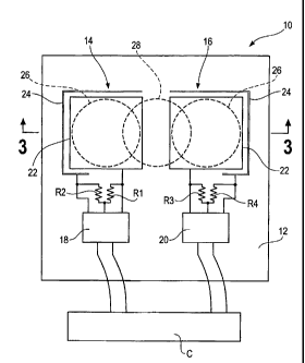
100071 Figure 1 is a plan view of a shared electrode pattern field effect
sensor
apparatus according to a first embodiment of the present invention;
100081 Figure 2 is a schematic diagram illustrating the electrical connections
among
the components on the sensor substrate of the apparatus of Figure 1;
[00091 Figure 3 is a cross-sectional view of the apparatus of Figure 1 taken
along line
3-3 and viewed in the direction of the arrows, with broken lines illustrating
electric flux lines;
CA 02594527 2007-06-22
WO 2006/071799 PCT/US2005/046870
3
[0010] Figure 4 is a plan view of a shared electrode pattern field effect
sensor
apparatus according to a second embodiment;
[0011] Figure 5 is a plan view of a shared electrode pattern field effect
sensor
apparatus according to a third embodiment;
[0012] Figure 6 is a plan view of a shared electrode pattern field effect
sensor
apparatus according to a fourth embodiment;
[0013] Figure 7 is a schematic diagram illustrating the electrical connections
among
the components on the sensor substrate of the apparatus of Figure 6;
[0014] Figure 8 is a plan view of a shared electrode pattern field effect
sensor
apparatus according to a fifth embodiment;
[0015] Figure 9 is a schematic diagram illustrating the electrical connections
among
the components on the sensor substrate of the apparatus of Figure 8; and
[0016] Figure 10 is a plan view of an inner electrode according to the fifth
embodiment.
DETAILED DESCRIPTION OF THE ILLUSTRATED EMBODIMENTS
[0017] Figure 1 illustrates a first preferred embodiment of a shared electrode
pattern
field effect sensor apparatus 10 according to the present invention. Apparatus
10 includes
first and second conductive electrode patterns 14, 16 disposed on dielectric
substrate 12.
Each electrode pattern is electrically coupled to a corresponding pulse
generation circuit and
a corresponding detection circuit. Preferably, the pulse generation and
detection circuits are
embodied as integrated control circuits 18, 20, which are disposed on
substrate 12 near the
corresponding electrode patterns 14, 16. A controller C receives output
signals from each
detection circuit. Controller C can, but need not be, disposed on substrate
12.
[0018] Substrate 12 may be formed from glass, plastic, fiberglass reinforced
epoxy
resin, or some other dielectric substance. Depending on the particular
application, substrate
CA 02594527 2007-06-22
WO 2006/071799 PCT/US2005/046870
4
12 may be either rigid or flexible, and may have either a substantially
uniform or varying
thickness including dimples or depressions. For example, a glass substrate 12
may have a
thickness of between about 1.1 mm and about 5 mm. A polymer substrate 12 may
have a
thickness of less than 1 mm. The thickness of substrate 12 may vary depending
on the
particular application such that a thicker substrate may be used where
additional strength is
required. Further, substrate 12 may be manufactured from a flexible material
for use in
applications where sensor apparatus 10 must conform to a non-planar shape.
Preferably,
substrate 12 is free of penetrations proximate electrode patterns 14, 16 and
corresponding
sense areas, as described below, so that contaminants present on one side of
substrate 12 do
not readily migrate to the other surface of substrate 12.
[00191 Each electrode pattern 14, 16 preferably has an inner electrode 22 and
an outer
electrode 24 partially surrounding inner electrode 22. Each inner electrode 22
defines a
primary sense area, as shown by dashed lines 26. A portion of inner electrode
22 of electrode
pattern 14 is adjacent a portion of inner electrode 22 of electrode pattern
16. The adjacent
portions of inner electrodes 22 of electrode patterns 14, 16 define a
secondary sense area, as
shown by dashed lines 28. Preferably, outer electrodes 24 do not extend into
the region
between inner electrodes 22 of adjacent electrode patterns 14, 16. Inner
electrodes 22 of
electrode patterns 14, 16 are arranged and spaced such that secondary sense
area 28 partially
overlaps a portion of each primary sense area 26 of adjacent patterns 14, 16.
[00201 While inner electrodes 22 are shown in Figure 1 as being substantially
rectangular, and outer electrodes 24 are shown as comprising linear segments,
other
geometric shapes may be used for inner and outer electrodes 22, 24. The
conductive material
surface area of inner electrode 22 can, but need not differ from the
conductive material
surface area of outer electrode 24. Electrodes 22, 24 can be made of any
suitable conductive
CA 02594527 2011-04-05
material, for example, copper, indium tin oxide, and other materials as would
be recognized
by one skilled in the art.
[0021) Integrated control circuits 18, 20 preferably are TS-100 ASICs, an
integrated
circuit available from TouchSensor Technologies, LLC of Wheaton, Illinois. The
general
principles of operation of the TS-100 ASIC are described in United States
Patent No.
6,320,282 to Caldwell. The pin-out of integrated circuits 18, 20 as shown in
the drawings corresponds to that of the TS-100 ASIC, where the input power
(+5 volts) connection is on pin 1, the ground connection is on pin 2, the
signal
output connection is on pin 3, outer electrode 24 connection is on pin 4, the
excitation signal connection is on pin 5, and inner electrode 22 connection is
on pin 6.
[0022] Referring to Figures 1 and 2, integrated control circuit 18 preferably
is
connected to inner and outer electrodes 22, 24 of electrode pattern 14 through
resistors RI,
R2, respectively. Likewise, integrated control circuit 20 is connected to
inner and outer
electrodes 22, 24 of electrode pattern 16 through resistors R3, R4,
respectively. In the
illustrated embodiments, resistors R1-R4 are external to, and connected to,
integrated control
circuits 18, 20. In other embodiments, resistors RI -R4 can be internally
provided within
integrated control circuits 18, 20.
[0023] In operation, excitation signals are provided to inner and outer
electrodes 22,
24 of each electrode pattern 14, 16 from pin 5 of the corresponding integrated
control circuit
18, 20. Preferably, an oscillator output pulse train or square wave signal is
provided at pin 5
to both inner electrode 22 and outer electrode 24. The oscillator signal may
be a square wave
oscillating between 0 and +5 volts at a frequency of approximately 32 kHz.
Alternatively,
the oscillator or strobe signal may have a frequency of up to or greater than
200 kHz,
depending on the detection circuitry used. Furthermore, the strobe signal may
oscillate
CA 02594527 2007-06-22
WO 2006/071799 PCT/US2005/046870
6
between 0 and +3 volts, 0 and +12 volts, 0 and +24 volts, -5 volts and +5
volts, or any other
voltage range.
[0024] The excitation signals applied to inner and outer electrodes 22, 24 of
each
electrode pattern 14, 16 generate electric fields about inner and outer
electrodes 22, 24. As
shown by the dashed lines in Figure 3, electric flux lines emanate from inner
and outer
electrodes 22, 24 and through substrate 12, such that electric fields
corresponding to each
inner and outer electrode 22, 24 emanate from primary sense areas 26 and
secondary sense
area 28. Although not shown in the drawings, electric flux lines would also
emanate from
inner and outer electrodes 18, 20 in the opposite direction, away from (rather
than through)
substrate 12. However, the electric flux concentration would be greater near
the sense areas
26, 28 on the side of substrate 12 opposite the electrode patterns, given that
the electric flux
concentration is multiplied through dielectric substrates, as would be
understood by one
skilled in the art. An insulator, such as a potting material, preferably is
applied to the
electrode pattern side of substrate 12 to shield or dissipate the electric
fields emanating away
from substrate 12. In other embodiments, an air gap or backing of foam rubber
or plastic
may be provided. These insulating structures reduce the likelihood of stimuli
on the side of
substrate 12 opposite sense areas 26, 28 from causing unintended sensor
actuation. These
insulating structures would be omitted in embodiments where sensing from both
sides of the
substrate is desired.
[0025] Preferably, inner and outer electrodes 22, 24 are charged such that all
of the
electric fields emanating therefrom have the same polarity. The fields extend
outwardly from
inner and outer electrodes 22, 24. Field strength is greatest closer to
electrodes 22, 24 (and,
therefore, substrate 12), and dissipates with distance from electrodes 22, 24.
Preferably, the
strength of the electric fields is substantially dissipated at a distance of
about 25 mm from the
CA 02594527 2007-06-22
WO 2006/071799 PCT/US2005/046870
7
exterior surface of substrate 12 proximate the corresponding sense area 26,
28. Voltage input
may be increased if stronger fields are desired.
[0026] Integrated control circuits 18, 20 and associated resistors R1-R4 are
configured so as to generate an electric field of predetermined strength about
each electrode
22, 24. The detection circuits embodied in integrated control circuits 18, 20
sense and
compare the strengths of the electric fields generated about inner and outer
electrodes 22, 24.
When an object or stimulus, for example, a user's fingertip or conductive
mass, is proximate
a sense area 26, the electric fields associated with the corresponding inner
and outer
electrodes 22, 24 are disturbed. (Preferably, the stimulus must be 25 mm or
closer to the
sense area 26 to disrupt the electric fields, given that the field strength
preferably is
substantially dissipated at greater distances.) Preferably, each integrated
control circuit 18,
20 produces an output signal indicating a touch only when it senses that the
disturbance to the
electric field about the corresponding inner electrode 22 exceeds the
disturbance to the
electric field about the corresponding outer electrode 24 by a predetermined
degree. This
output signal is sent to controller C for further processing, as discussed
further below.
[0027] Typically, contaminants and debris would affect the electric fields
about both
inner and outer electrodes 22, 24 equally. Because at least the foregoing
threshold difference
in field disturbance must be achieved in order for integrated control circuit
18, 20 to output a
signal indicating an intentional touch, unintended responses causes by
contaminants are
minimized. Similarly, unintended responses resulting from stimuli proximate
the periphery
of sense area 26 disturbing the electric field about outer electrode 24 to a
greater degree than
the electric field about inner electrode 22 are minimized.
[0028] Electrode patterns 14, 16 are arranged such that the presence of a
stimulus
proximate one of primary sense areas 26 affects the field associated with the
corresponding
electrode pattern 14, 16, causing the corresponding integral control circuit
18, 20 to output a
CA 02594527 2007-06-22
WO 2006/071799 PCT/US2005/046870
8
signal indicative of an intentional touch (a "touch signal"). The presence of
an object
proximate secondary sense area 28 affects the fields associated with the inner
electrodes 22 of
both of electrode patterns 14 and 16 to a greater degree than the electric
fields associated with
the corresponding outer electrodes 24, causing both integrated control
circuits 18 and 20 to
substantially simultaneously output a touch signal. Based on the touch signals
it receives
from integrated control circuits 18 and 20, controller C can determine which,
if any, of sense
areas 26, 28 is touched or otherwise stimulated at a given time. In response,
controller C can
generate a corresponding control signal. For example, controller C can
generates a first
control signal in response to a touch signal received only from integrated
control circuit 18, a
second control signal in response to a touch signal received only from
integrated control
circuit 20, and a third control signal in response to touch signals received
substantially
simultaneously from both integrated control circuits 18, 20. Thus, the present
invention
allows a controller to generate three distinct and specific control signals
based on input
received from only two sense electrode patterns 14, 16 and corresponding
integrated control
circuits 18, 20.
[00291 In a preferred embodiment, electrode patterns 14, 16 are configured so
that
primary sense areas 26 are sufficiently sized to receive a human fingertip.
For example,
primary sense area 26 may have a diameter of between about 8 mm and about 10
mm.
Likewise, secondary sense area 28 is sufficiently sized to receive a
fingertip. Inner electrodes
22 of first and second patterns 14, 16 are arranged so that a user's fingertip
overlaps inner
electrodes 22 associated with both of patterns 14, 16 when the fingertip is
within secondary
sense area 28. In other embodiments, sense areas 14, 16, can be sized as
required by the
specific application.
[00301 Various configurations and arrangements of electrode patterns 14, 16
may be
provided depending on the particular application. Further, three or more
electrode patterns
CA 02594527 2007-06-22
WO 2006/071799 PCT/US2005/046870
9
may be configured such that at least two corresponding detection circuits may
be
simultaneously triggered when a stimulus is simultaneously proximate the
corresponding
secondary sense area defined by two or more of the electrode patterns. Various
exemplary
embodiments of shared electrode patterns will now be described.
[0031] A shared sense electrode pattern touch sensor apparatus 40 according to
a
second embodiment of the present invention is best shown in Figure 4.
Apparatus 40
includes three linearly spaced electrode patterns 42, 44, 46 disposed on
substrate 12. Each
pattern 42, 44, 46 is electrically coupled to an associated pulse generation
and detection
circuit which preferably is embodied on an integrated control circuit (not
shown), as
described above. Each pattern 42, 44, 46 includes an inner electrode 48 and an
outer
electrode 50. An excitation signal is applied to each of inner and outer
electrodes 48, 50,
creating electric fields about each of inner and outer electrodes 48, 50, as
described above.
[0032] Each inner electrode 48 includes a primary portion 48A which in essence
defines a primary sense area, as shown by dashed lines 26a. Inner electrodes
48 of patterns
42, 46 also include one secondary portion 48B which in essence defines a
portion of a
secondary sense area. Inner electrode 48 of pattern 44 includes two secondary
portions 48B,
one of which is adjacent secondary portion 48B of electrode pattern 42 and the
other of which
is adjacent secondary portion 48B of electrode pattern 46. Adjacent secondary
portions 48B
define first and second secondary sense areas, as shown by dashed lines 28a.
[0033] Electrode patterns 42-46 and, therefore, primary and secondary sense
areas
26a, 28a may be linearly arranged, as shown in the drawings. In other
embodiments, the
electrode patterns and sense areas may be configured non-linearly by, for
example, modifying
the geometry of the inner and outer electrodes, as would be recognized by one
skilled in the
art. Primary and secondary sense areas 26a, 28a should be sufficiently sized
to receive a
stimulus, for example, a human fingertip. When a stimulus is introduced
proximate one of
CA 02594527 2007-06-22
WO 2006/071799 PCT/US2005/046870
primary sense areas 26a, the electric field about primary portion 48A of inner
electrode 48 of
the corresponding electrode pattern 42, 44, 46 is disrupted, and the
corresponding detection
circuit outputs a touch signal, as described above. When a stimulus is
introduced proximate
one of secondary sense areas 28a, the electric fields about secondary portions
48B of inner
electrodes 48 of corresponding electrode patterns 42, 44, 46 are disrupted,
and both
corresponding detection circuits output a touch signal, as described above.
[0034] As in the first embodiment described above, the detection circuit
associated
with each electrode pattern is electrically coupled to a controller (not
shown), which may be
disposed on substrate 12 or elsewhere. The controller generates a control
signal based on the
touch signals it receives from the detection circuits corresponding to
electrode patterns 42,
44, 46, as discussed above. Thus, apparatus 40 provides five input points or
sense areas
(three primary and two secondary sense areas) using only three electrode
patterns and three
associated integrated control circuits. In a preferred embodiment, apparatus
40 is used as a
digital slider control device having five command points or "levels" of
gradation.
[0035] A shared sense electrode pattern touch sensor apparatus 60 according to
a third
embodiment is best shown in Figure 5. Apparatus 60 includes five electrode
patterns 62, 64,
66, 68, 70 disposed in a linear arrangement on substrate 12. In alternate
embodiments,
electrode patterns 62-70 could be arranged in a non-linear pattern, as
discussed above. Each
electrode pattern 62-70 is electrically coupled to an associated pulse
generation and detection
circuit which preferably is embodied on an integrated control circuit (not
shown), as
described above. Electrode patterns 62 and 70 are disposed at opposite ends of
this linear
arrangement. Each end pattern 62, 70 includes an inner electrode 72 and an
outer electrode
74. Patterns 64, 66, 68 are disposed intermediate end patterns 62 and 70. Each
intermediate
pattern 64, 66, 68 includes an inner electrode 72A and first and second outer
electrodes 74A,
74B. As in the other embodiments discussed above, excitation signals are
applied to all inner
CA 02594527 2007-06-22
WO 2006/071799 PCT/US2005/046870
11
and outer electrodes 72, 72A, 74, 74A, 74B, which create electric fields
emanating therefrom.
The fields preferably have the same polarity so that the fields repel each
other, extending
outwardly toward infinity.
[00361 Each inner electrode 72, 72A defines a primary sense area, as shown by
dashed lines 26b. Adjacently disposed portions of inner electrodes 72, 72A
define secondary
sense areas, as shown by dashed lines 28b. For example, adjacent portions of
inner electrode
72 of end pattern 62 and inner electrode 72A of intermediate pattern 64 define
a first
secondary sense area 28b, and adjacent portions of inner electrodes 72A of
intermediate
patterns 64, 66 define a second secondary sense area 28b. Thus, five primary
sense areas 26b
and four secondary sense areas 28b are provided.
[00371 Primary and secondary sense areas 26b, 28b should be sufficiently sized
to
receive the particular stimulus to be used to disturb the electric fields
about sense areas 26b,
28b, for example, a human fingertip. When a stimulus is proximate one of
primary sense
areas 26b, the electric field emanating from the corresponding inner electrode
72, 72A is
disturbed, thereby triggering the corresponding detection circuit. When a
stimulus is
proximate one of secondary sense areas 28b, the electric fields emanating from
inner
electrodes 72, 72A of the two corresponding electrode patterns 62-70 are
disturbed, thereby
triggering the two corresponding detection circuits.
[00381 As in the embodiments described above, the detection circuit associated
with
each electrode pattern is electrically coupled to a controller (not shown),
which may be
disposed on substrate 12 or elsewhere. The controller generates a control
signal based on the
touch signals it receives from the detection circuits, as discussed above.
Thus, apparatus 60
provides nine input points using only five electrode patterns and five
associated integrated
control circuits. In a preferred embodiment, apparatus 60 is used as a digital
slider control
device having nine command points or "levels" of gradation.
CA 02594527 2007-06-22
WO 2006/071799 PCT/US2005/046870
12
[0039] A shared sense electrode pattern touch sensor apparatus 80 according to
a
fourth embodiment is best shown in Figure 6. Apparatus 80 includes four
peripherally
spaced electrode patterns 82, 84, 86, 88, and one central electrode pattern 90
disposed on
substrate 12. Peripheral patterns 82-88 are arranged in a circular
configuration, and central
electrode 90 is provided in a center of the circular configuration.
[0040] Each peripheral pattern 82-88 includes an inner electrode 92 and an
outer
electrode 94. Each inner electrode 92 includes a primary portion in essence
defining a
primary sense area 26c, and a secondary portion in essence defining a portion
of a secondary
sense area. Outer electrodes 94 preferably are peripherally spaced around the
circular
configuration and radially aligned with a corresponding primary sense area
26c.
[0041] Central pattern 90 includes an inner electrode 92A having a primary
portion
defining a primary sense area 26c' and four secondary portions adjacent
secondary portions of
each of inner electrodes 82-88 to define four secondary sense areas 28c.
Central pattern 90
also includes an outer electrode 94A proximate inner electrode 92A.
[0042] As in the other embodiments described above, each electrode pattern is
coupled to a pulse generation circuit and a detection circuit, both of which
preferably are
embodied on a TS-100 ASIC or other integrated control circuit. An excitation
signal is
applied to all inner and outer electrodes 92, 92A, 94, 94A, creating electric
fields emanating
therefrom. The fields preferably have the same polarity so that the fields
repel each other,
extending outwardly toward infinity.
[0043] Primary sense areas 26c, 26c' are sufficiently sized to receive a
stimulus, such
as a fingertip. When a stimulus is proximate one of primary sense areas 26c or
26c', the
electric field emanating from inner electrode 92 or 92A of the corresponding
pattern 82-90 is
disrupted, thereby causing the corresponding detection circuit to output a
touch signal. When
a stimulus is proximate one of secondary sense areas 28c, the electric fields
emanating from
CA 02594527 2007-06-22
WO 2006/071799 PCT/US2005/046870
13
adjacent inner electrodes 94, 94A of the corresponding one of peripheral
patterns 82-88 and
central pattern 90 are disrupted, thereby causing the two corresponding
detection circuits to
output touch signals.
[0044] Similar to the embodiments described above, the detection circuit
associated
with each electrode pattern is electrically coupled to a controller C', which
may be disposed
on substrate 12 or elsewhere. The controller generates a control signal based
on the touch
signals it receives from the detection circuits, as discussed above.
[0045] Apparatus 80 may also include light-emitting diodes L1-L5 or other
light
sources disposed on substrate 12, as illustrated schematically in Figure 7.
Light-emitting
diodes L1-L5 preferably are illuminated when the corresponding detection
circuit outputs a
touch signal.
[0046] In a preferred embodiment, apparatus 80 is a navigational control
device for
use with microprocessor Chaving an associated display. Apparatus 80 preferably
includes a
base for housing the electrical components and electrodes of apparatus 80.
Electrode patterns
82-90 and the associated components 95 may be provided on the back surface 12A
of a
transparent substrate 12, so that the opposing front surface 12B acts as the
touch surface for a
user. The touch surface may include graphical designs aligned with primary and
secondary
sense areas 26c, 26c', 28c. For example, directional arrows and a center
button may be
provided on the touch surface. Alternatively, a thin layer, such as a film,
including such
graphical designs may be adhered to the touch surface 12B.
[0047] Apparatus 80 can be used to provide directional control commands to,
for
example, move an object in a display in X-, Y- coordinates relative to the
display. Referring
to Figures 6 and 7, a touch (or other stimulus) proximate primary sense area
26c
corresponding to electrode pattern 82 causes the corresponding detection
circuit (embodied in
corresponding integrated control circuit 95) to output a touch signal to
controller C. In
CA 02594527 2007-06-22
WO 2006/071799 PCT/US2005/046870
14
response, controller C' generates a directional command for "up", as shown by
arrow U.
Similarly, touches proximate primary sense areas 26c corresponding to
electrode pattern 84,
86, 88, cause the corresponding detection circuits to output touch signals to
Controller C'. In
response, controller C' generates directional commands for "right," "down,"
and "left,"
respectively, as shown by arrows R, D, and L, respectively.
[0048] A touch proximate secondary sense area 28C corresponding to electrode
patterns 82, 90 causes both corresponding detection circuits to output touch
signals to
Controller C'. In response, controller C' generates a directional command for
"diagonally up
and to the right", as shown by arrow U-R. Similarly, touches proximate
secondary sense
areas 28c corresponding to electrode patterns 84, 90, electrode patterns 86,
90, and electrode
patterns 88, 90, will, respectively, cause controller C' to generate
directional commands for
"diagonally down and to the right," as shown by arrow D-R, diagonally down and
to the left,"
as shown by arrow D-L, and "diagonally up and to the left," as shown by arrow
U-L. A
touch proximate sense area 26c' will cause only the detection circuit
corresponding to center
electrode pattern 90 to output a touch signal, which controller C' may
interpret as a command
to, for example, start or stop movement. A shared sense electrode pattern
touch sensor
apparatus 100 according to a fifth embodiment is best shown in Figure 8.
Apparatus 100
includes four peripherally spaced electrode patterns 102, 104, 106, 108
disposed on substrate
12 and arranged in a circular configuration. Each pattern 102-108 is
electrically coupled to a
pulse generation circuit and a detection circuit which preferably are embodied
as a TS-100
ASIC or other integrated control circuit, as described above and as best shown
in Figure 9.
[0049] Each pattern 102-108 includes an inner electrode 110 and an outer
electrode
112. As best shown in Figure 10, each inner electrode 110 includes a primary
portion 114,
first and second side portions 116, 118, and a center portion 120. Each outer
electrode 112 is
CA 02594527 2007-06-22
WO 2006/071799 PCT/US2005/046870
peripherally spaced around the circular configuration, and radially aligned
with a
corresponding primary portion 114, as best shown in Figure 8.
[0050] Inner electrodes 110 are arranged such that first side portion 116 of
one of
patterns 102-108 is adjacent second side portion 118 of another of patterns
102-108. Center
portions 120 from each of patterns 102-108 are disposed in a center portion of
the circular
configuration. Primary portions 114 define a primary sense area, as shown by
dashed circles
26d. Each pair of adjacent side portions 116, 118 define a secondary sense
area, as shown by
dashed circles 28d. The center portion defines a tertiary sense area, as shown
by dashed
circle 122. Each sense area 26d, 28d, 122 is sufficiently sized to receive a
stimulus, such as a
human fingertip.
[0051] The output of each detection circuit preferably is coupled to a
controller C", as
best shown in Figure 9. Controller C" generates an output signal as a function
of the touch
signals it receives from the various detection circuits. Apparatus 100 may
also include light-
emitting diodes, such as provided in the fourth embodiment.
[0052] In a preferred embodiment, apparatus 100 is a navigational control
device for
use with a microprocessor C" having an associated display. Apparatus 100
preferably
includes a base for housing the electrical components and a substrate 12
having directional
arrows and a center button on the touch surface, as described above.
[0053] Nine command points are provided using four electrode patterns and four
components, as best shown in Figures 8 and 9. Control commands providing
directional
information may then move an object in X-, Y- coordinates relative to the
display, or change
the orientation of images on the display. Because each inner electrode 110
includes center
portion 120, a separate centrally disposed electrode pattern is not required,
such as provided
in the fourth embodiment.
CA 02594527 2007-06-22
WO 2006/071799 PCT/US2005/046870
16
[0054] Referring to Figure 8, a user's finger or other stimulus proximate one
of
secondary sense areas 28d causes both corresponding detection circuits to
output touch
signals to controller C". In response, controller C" generates a corresponding
directional
command for "up", "right", "down", or "left", as shown by arrows U, R, D, L,
respectively.
A user's finger proximate one of primary sense areas 26d causes only the one
corresponding
detection circuit to output a touch signal to controller C". In response,
controller C"
generates a corresponding directional command for "diagonally up and to the
right",
"diagonally down and to the right", "diagonally down and to the left", and
"diagonally up and
to the left", as shown by arrows U-R, D-R, D-L, U-L, respectively. A user's
finger proximate
tertiary sense area 122 causes the detection circuits corresponding to all
four electrode
patterns to output a touch signal to controller C". In response, controller C'
generates a
command to, for example, "start movement" or "stop movement."
[0055] It should be understood that the embodiments disclosed herein are
exemplary
only, and the present invention is not so limited. The present invention may
be used for
various other applications. Further, various control signals may be generated
by an
associated controller. In addition, aspects of one of the embodiments may be
incorporated
into another of the embodiments. The shared electrode patterns of the present
invention
allow for a reduction in the number of components required for multiple sense
points, thereby
decreasing manufacturing costs. Furthermore, the present invention provides
for increased
functionality for applications having limited space.
[0056] Thus, various modifications and configurations of the present invention
may
be made without departing from the scope or spirit of the present invention.
For example, a
shared electrode pattern may include an inner electrode having more than three
secondary
portions. Accordingly, the present invention is intended to include all such
modifications and
variations, provided they come within the scope of the following claims and
their equivalents.