Note: Descriptions are shown in the official language in which they were submitted.
CA 02594683 2007-07-10
WO 2006/083500 PCT/US2006/000768
ARRAY ANTENNA INCLUDING A MONOLITHIC ANTENNA
FEED ASSEMBLY AND RELATED METHODS
Background of the Inve-ztion
Existing phased array antennas include a wide
variety of configurations for various applications, such as
satellite reception and remote broadcasting. The desirable
characteristics of low cost, light-weight, low profile and
mass producibility are provided in general by printed circuit
antennas. Printed circuit antennas are defined by flat
conductive elements spaced from a single, essentially
continuous ground element by a dielectric sheet of uniform
thickness.
While a printed circuit antenna is advantageous in
applications requiring a conformal configuration, e.g., in
aerospace systems, mounting the antenna presents challenges.
One of these challenges is with respect to the manner in which
it is fed such that conformality and satisfactory radiation
coverage and directivity are maintained and losses to
surrounding surfaces are reduced.
An antenna feed assembly for a phased array antenna
with a wide frequency bandwidth and a wide scan angle is
disclosed in U.S. Patent No. 6,483,464. The '464 patent is
assigned to the current assignee of the present invention, and
is incorporated herein by reference in its entirety. In
particular, this antenna can be conformally mounted to a
surface, and the antenna feed assembly includes a respective
feed line organizer body having passageways therein for
receiving the respective coaxial feed lines for a
corresponding antenna element. Each respective feed line
organizer body is individually coupled to the ground plane
using four screws. Although this patent discloses a
significant advance in such antennas, inlividually coupling
the feed line organizer bodies to the ground plane is a
-1-
CA 02594683 2007-07-10
WO 2006/083500 PCT/US2006/000768
tedious and time consuming process, especially when the phased
array antenna includes a large number of antenna elements. In
addition, manufacturing costs may be increased as a result of
this process.
Summary of the Invention
In view of the foregoing background, it is therefore
an object of the present invention to provide an array antenna
that is relatively straightforward to produce, particularly
with respect to the antenna feed assembly.
This and other objects, features, and advantages in
accordance with the present invention are provided by an
antenna comprising a plurality of antenna elements, an antenna
feed assembly, and at least one integrated circuit adjacent
the antenna feed assembly on a side thereof opposite the
antenna elements and connected thereto via the antenna feed
assembly.
The antenna feed assembly may comprise a conductive
base plate spaced from the plurality of antenna elements, and
the conductive base plate has a plurality of feed openings
therein. A plurality of spaced apart conductive posts are
integrally formed with the conductive ba.3e plate as a
monolithic unit, and extend outwardly therefrom toward the
plurality of antenna elements. Each conductive post may have
at least one passageway therethrough aligned with at least one
respective feed opening in the conductive base plate to define
at least one antenna feed passageway. A respective elongated
feed conductor may extend through each antenna feed
passageway.
The conductive base plate functions as a ground
plane for the plurality of antenna elements. Since each
conductive post is integrally formed with the conductive base
plate as a monolithic unit, this advantageously allows the
antenna feed assembly to be formed in a relatively
-2-
CA 02594683 2007-07-10
WO 2006/083500 PCT/US2006/000768
straightforward manner. For example, the antenna feed
assembly may be machined from a block of conductive material.
The cost of an antenna with an antenna feed assembly machined
from a block of conductive material may be significantly
reduced. Moreover, since the conductive posts and the
conductive base plate are formed as a monolithic unit, the
antenna feed assembly is more reliable, particularly during
periods of extreme vibration.
The plurality of antenna elements may comprise first
and second sets of orthogonal antenna elements to provide dual
polarization. For a dual polarization, ~ach conductive post
has four passageways for interfacing with a respective first
and second set of orthogonal antenna elements.
The antenna may further comprise a dielectric layer
between the plurality of antenna elements and the conductive
base plate. The antenna has a desired frequency range, and
the dielectric layer has a thickness that is equal to or less
than one-half a wavelength of a highest desired frequency.
The at least one integrated circuit may comprise a
plurality of active Balun integrated circuits. The active
Balun integrated circuits advantageously provide impedance
matching with the antenna elements. In addition, the Baluns
replace the 0/180 degree hybrid circuits normally used with
this type of antenna - which resulted in a 3 dB power loss.
Moreover, in addition to overcoming this power loss, the Balun
integrated circuits may also comprise low noise amplifiers.
The antenna may further comprise a beam forming
network layer coupled to the active Balun integrated circuits
so that the antenna is a phased array antenna. The beam
forming network layer is based upon strip lines sandwiched
between ground planes, and replaces the coaxial cables
normally associated with this type of antenna. The advantages
are two-fold. First, the thickness of the beam forming
network layer is smaller by about a factor of six as compared
-3-
CA 02594683 2007-07-10
WO 2006/083500 PCT/US2006/000768
to the use of coaxial cables. Second, trie strip lines help to
dissipate heat away from the antenna elements and the active
Balun integrated circuits.
The antenna may further comprise at least one time
delay integrated circuit coupled to the beam forming network
layer. The time delay integrated circuits may be programmable
to define a scan angle of about +50 degrees.
The antenna may further comprise a power and control
distribution network layer coupled to the active Balun
integrated circuits and the beam forming network layer. The
array of antenna elements is sized and relatively positioned
so that the antenna is operable over a frequency range of 2 to
18 GHz. The antenna has an overall thickness that is less than
or equal to about 1 inch.
Another aspect of the present invention is directed
to a method for making an antenna as described above. The
method comprises forming a plurality of antenna elements,
forming an antenna feed assembly, and connecting at least one
integrated circuit to the plurality of antenna elements via
the antenna feed assembly. The at least one integrated
circuit may be adjacent the antenna feed assembly on a side
thereof opposite the plurality of antenna elements.
More particularly, forming the antenna feed assembly
comprises forming a conductive base plate spaced from the
plurality of antenna elements and having a plurality of feed
openings therein, and forming as a monolithic unit a plurality
of spaced apart conductive posts with the conductive base
plate. The plurality of spaced apart conductive posts extend
outwardly from the conductive base plate toward the plurality
of antenna elements. Each conductive post may have at least
one passageway therethrough aligned with at least one
respective feed opening to define at least one antenna feed
passageway connecting the at least one integrated circuit to
-4-
CA 02594683 2007-07-10
WO 2006/083500 PCT/US2006/000768
the plurality of antenna elements via the antenna feed
assembly.
Brief Description of the Orawings
FIG. 1 is a top schematic plan view of a dual
polarization phased array antenna in accordance with the
present invention.
FIG. 2 is an exploded perspective view of the dual
polarization phased array antenna illustrated in FIG. 1.
FIG. 3 is a top plan view of the antenna feed
assembly illustrated in FIG. 2.
FIG. 4 is a side view of the antenna feed assembly
illustrated in FIG. 2.
FIG. 5 is a partial cross-sectional side view of the
phase array antenna in accordance with the present invention.
Detailed Description of the Preferred Embodiments
The present invention will now be described more
fully hereinafter with reference to the accompanying drawings,
in which preferred embodiments of the invention are shown.
This invention may, however, be embodied in many different
forms and should not be construed as limited to the
embodiments set forth herein. Rather, these embodiments are
provided so that this disclosure will be thorough and
complete, and will fully convey the scope of the invention to
those skilled in the art. Like numbers refer to like elements
throughout.
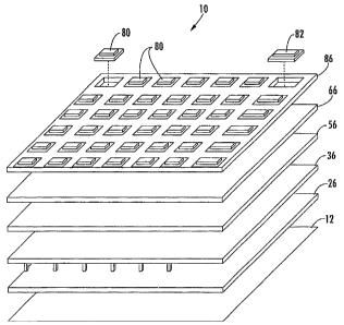
Referring initially to FIG. 1, an antenna 10
according to the invention includes a plurality of antenna
units 12 arranged in an array. The illustrated antenna 10
includes 36 antenna units 12 formed on a printed conductive
sheet 14, where each antenna unit includes four adjacent
dipole antenna elements 16, 18, 20, 22 arranged in a spaced
apart relation from one another about a central feed position
-5-
CA 02594683 2007-07-10
WO 2006/083500 PCT/US2006/000768
24. The 36 antenna units 12 are for illustrative purposes
only, and the antenna 10 may include a larger number of
antenna units, such as 250 or more, for example.
The four adjacent antenna elements 16-22 for each
antenna unit 12 may be arranged as first and second sets of
orthogonal antenna elements, e.g., 16/22 and 18/20, to provide
dual polarization. Of course, only a single pair of antenna
elements, e.g., 16/22, may be used to provide for a single
polarization embodiment.
The array of antenna units 12 are sized and
relatively positioned so that the antenna 10 is operable over
a desired frequency range, such as 2 to 18 GHz, for example,
which is a 9:1 bandwidth. Of course, the antenna units 12 may
be sized and positioned to support other frequency bands,
including frequency bands with a larger bandwidth. For a more
detailed discussion on the different features and embodiments
of the antenna units, reference is directed to U.S. Patent No.
6,512,487. The '487 patent discloses dipole antenna elements
and is assigned to the current assignee of the present
invention, and is incorporated herein by reference in its
entirety.
The antenna 10 will now be discussed with reference
to FIGS. 2-5. The antenna 10 is made up of a plurality of
layers. The different layers are fabricated by standard PCB
techniques, and the antenna 10 can be conformally mounted to a
desired surface as readily abpreciated by those skilled in the
art. The outermost layer is the array of antenna units 12
carried by the printed conductive sheet 14. A dielectric
layer 26 is between the printed conductive sheet 14 and an
antenna feed assembly 36. The dielectric layer 26 has a
thickness that is typically equal to or less than about one-
half a wavelength of a highest desired frequency, e.g., 18
GHz.
-6-
CA 02594683 2007-07-10
WO 2006/083500 PCT/US2006/000768
The antenna feed assembly 36 comprises a conductive
base plate 38 spaced from the array of antenna elements 16-22,
and the conductive base plate has a plurality of feed openings
40 therein. A plurality of spaced apart conductive posts 42
are integrally formed with the conductive base plate 38 as a
monolithic unit, and extend outwardly therefrom toward the
plurality of antenna elements 16-22. Each conductive post 42
has a plurality of passageways therethrough 46 that are
aligned with a plurality of respective feed opening 40 in the
conductive base plate 38 to define a plurality of antenna feed
passageways.
A respective elongated feed conductor 50 extends
through each antenna feed passageway. For dual polarization,
each conductive post 42 has four passageways 46 therethrough
for interfacing with a respective first and second set of
orthogonal antenna elements 16/22 and 18/20, and a respective
elongated feed conductor 50 extends through each passageway
46. A distance that each conductive post 42 extends from the
conductive base plate 38 is based on the highest operating
frequency of the antenna 10, i.e., one-half the wavelength of
the highest desired frequency. The thickness of the
dielectric layer 24 and the distance the conductive posts 42
extend from the conductive base plate 38 are substantially
equal.
The conductive base plate 38 functions as a ground
plane for the plurality of antenna elements 16-22. Since each
conductive post 42 is integrally formed aith the conductive
base plate 38 as a monolithic unit, this advantageously allows
the antenna feed assembly 36 to be formed in a relatively
straightforward manner. For example, the antenna feed assembly
36 may be machined from a solid block of conductive material,
such as brass.
The cost of an antenna 10 with an antenna feed
assembly 36 that is machined from a solid block of conductive
-7-
CA 02594683 2007-07-10
WO 2006/083500 PCT/US2006/000768
material may be significantly reduced. The weight is also
reduced. Moreover, since the conductive posts 42 and the
conductive base plate 38 are formed as a monolithic unit, the
antenna feed assembly 36 is more reliable, particularly during
periods of extreme vibration. The common mode normally
associated with multiple feed structures is also reduced.
Each conductive post 42 is illustrated as being
rectangular shaped, although other shapes are acceptable. An
example diameter d of each respective passageway 46
therethrough is 0.028 inches. An example distance x between a
center of any two passageways 46 is 0.048 inches. A
corresponding width w of the sides 43 of each conductive post
42 is 0.100 inches. The antenna feed assembly 36 also
includes a plurality of alignment posts 52 used in assembling
together the plurality of layers of the antenna 10.
A DC power and control distribution network layer 56
is adjacent the antenna feed assembly 36. The DC power and
control distribution network layer 56 includes a ground plane
58 and typically 2 or more DC/control layers 60, as best
illustrated in FIG. S.
A beam forming network layer 66 is adjacent the DC
power and control distribution network layer 56, and a
plurality of integrated circuits 80 are connected to the beam
forming network layer so that the antenna 10 is a phased array
antenna. The beam forming network layer 66 includes couplers,
i.e., a summing network, for summing the signals from the
antenna elements 16-22. The beam forming network layer 66 is
based upon strip lines 68 sandwiched between ground planes 70
and 72, as illustrated in FIG. 5, and replaces the coaxial
cables normally associated with this type of antenna. The
advantages are two-fold. First, the thi--kness of the beam
forming network layer 66 is smaller by about a factor of six
as compared to the use of coaxial cables. Second, the strip
-8-
CA 02594683 2007-07-10
WO 2006/083500 PCT/US2006/000768
lines help to dissipate heat away from the antenna elements
16-22 and the integrated circuits 80.
The integrated circuits 80 comprise a plurality of
active MMIC Balun integrated circuits. The Balun integrated
circuits 80 advantageously provide impedance matching, e.g.,
50 ohms, between the antenna elements 16-22 and the beam
forming network layer 66. Each Balun integrated circuit may
further comprise a low noise amplifier for amplifying signals.
There is an active Balun integrated circuit 80 for each
antenna unit 12.
In addition, the Balun integrated circuits 80
replace the 0/180 degree hybrid circuits normally used with
this type of antenna. The 0/180 degree hybrid circuits are
passive devices, and there was typically a 3 dB power loss
associated with these circuits. Not only do the active MMIC
Balun integrated circuits 80 avoid this 3 dB power loss, but
they also reduce the effects of any loses associated with the
strip lines 68 in the beam forming network layer 66.
Insertion loss is also reduced and the active Balun integrated
circuits 80 also provide an improved noise figure because of
the low noise amplifiers included therein.
The antenna 10 may further comprise a plurality of
time delay integrated circuits 82 coupled to the beam forming
network layer 66. The time delay integrated circuits add up
in phase all the signals arriving at each individual antenna
element 16-22. The time delay integrated circuits 82 may be
programmable so that the phased array antenna is operable over
a scan angle of about +50 degrees, for example. The time
delay integrated circuits 82 may be 6 bit integrated circuits,
for example. A ribbon 90 connects the integrated circuits 80,
82 to the DC power and control distribution network layer 56.
The illustrated antenna 10 is compact, and has an
overall thickness that is less 1 inch, and more particularly,
is about 0.7 inches. The 0.7 inches overall thickness is
-9-
CA 02594683 2007-07-10
WO 2006/083500 PCT/US2006/000768
based upon the integrated circuits 80, 82 being recessed
within the dielectric layer 86 carrying the integrated
circuits so that the upper surface of these integrated
circuits is flush with the upper surface of the dielectric
layer.
Another aspect of the present invention is directed
to a method for making an antenna 10 as described above. The
method comprises forming a plurality of antenna elements 16-
22, forming an antenna feed assembly 36, and connecting at
least one integrated circuit 80 to the plurality of antenna
elements via the antenna feed assembly. The at least one
integrated circuit 80 is adjacent the antenna feed assembly 36
on a side thereof opposite the plurality of antenna elements
16-22.
More particularly, forming the antenna feed assembly
36 comprises forming a conductive base plate 38 spaced from
the plurality of antenna elements 16-22 and having a plurality
of feed openings 40 therein, and forming as a monolithic unit
a plurality of spaced apart conductive posts 42 with the
conductive base plate. The plurality of spaced apart
conductive posts 42 extend outwardly from the conductive base
plate 38 toward the plurality of antenna elements 16-22. Each
conductive post 42 has at least one passageway 46 therethrough
aligned with at least one respective feed opening 40 to define
at least one antenna feed passageway connecting the at least
one integrated circuit 80 to the plurality of antenna elements
16-22 via the antenna feed assembly 36.
-10-