Note: Descriptions are shown in the official language in which they were submitted.
CA 02594884 2011-01-14
IMAGING APPARATUS FOR FULLYAUTOMATIC SCREEN PRINTER
FIELD OF THE INVENTION
The present invention relates to an imaging apparatus, specially relates to an
imaging apparatus for the reference mark measurement and inspecting the paste
solder
printing; more specially relates to an imaging apparatus for the reference
mark
measurement of the screen and the printed circuit board during the paste
solder printing
of the printed circuit board of the screen printing process, and for the
inspection of the
screen and the printed circuit board during the paste solder printing.
BACKGROUND OF THE INVENTION
During the paste solder printing of the printed circuit board of the screen
printing
process, in order to apply the solder paste to the printed circuit board
accurately, the
portions of the printed circuit board desired to be printed are required to be
corresponding
to the holes of the screen. Reference mark measurement is usually used for the
alignment of the screen and the printed circuit board, that is to say, signs
are marked on
both the screen and the printed circuit board so as to ensure that the
portions of the
printed circuit board desired to be printed are corresponding to the holes of
the screen
when the relevant signs of the screen are calibrated with respect to that of
the printed
circuit board. The simplest method of the alignment is mechanical positioning,
in which
the reference marks are the holes formed on the printed circuit board, and the
sinker bars
of the pistons of one or more cylinder-piston means are inserted into the
positioning holes
of the printed circuit board when positioning. However, this method is of the
defects
including low precision, low speed and even that there is no positioning hole
due to the
different positioning aperture of different printed circuit board. Therefore,
this method is
difficult to adapt to the development of the SMT production with high density,
large output
and high precision, and will fall into disuse gradually.
I
CA 02594884 2007-07-26
With the development of the electronic component in the direction of
micromation,
chip type and high density, the screen printer is required to be of higher
precision, speed
and reliability. Currently, in the SMT product line of the printed circuit
board with high
density, most of the defects come from the printing faults of the solder
paste. The quality
inspection of the solder-paste printing is mainly carried out by manual
inspection. The
manual inspection may have the problems including strong subjectivity, poor
reproducibility, misjudgment and overlook due to vision fatigue, etc. The
manual
inspection is hardly qualified for the inspection requirement of SMT product
line.
A screen printer utilizing machine vision technique can realize simultaneously
both
alignment with respect to the reference mark in high speed and high precision,
and
printing quality inspection during printing. At present, the imaging apparatus
of the screen
printer of this type normally includes a low-angle ring light source, two
light sources, a
beamsplitter, an optical reflector, an imaging lens and an image sensor.
During the
operation, the two light sources on different horizontal planes illuminate at
different time,
the light sources irradiate on the screen or the printed circuit board through
the
beamsplitter, and then the beams of light are reflected back to the
beamsplitter and
refracted to the imaging lens by the beamsplitter, and finally imaging on the
image sensor
is obtained. This method is of the advantages including simple light path and
low cost.
However, acquiring the images at different time may result in that the image
acquiring
positions of the lower image and the upper image are inconsistent; and the
dimension of
the apparatus in the direction of the upward and downward light path is too
large, so that
the distance between the printed circuit board and the screen is accordingly
large when
acquiring the image.
SUMMARY OF THE INVENTION
An object of the present invention is to provide an imaging apparatus with
compact
structure, in which the light path is easy to adjust and the images can be
acquired from
the same position in upward and downward directions. The apparatus is used for
image
acquiring during the reference mark measurement of the screen and the printed
circuit
board, and during the inspection in the solder-paste printing process.
The above object of the present invention is achieved by the following
technical
solutions:
2
CA 02594884 2007-07-26
An imaging apparatus for fully automatic screen printer including two stacked
light
sources, two stacked beamsplitters, two stacked optical reflectors, two
stacked imaging
lens and two stacked image sensors, wherein the two stacked optical reflectors
and the
two stacked light sources are correspondingly disposed on two different sides
of the two
beamsplitters, the two stacked imaging lens are disposed on another side of
the
beamsplitters different from that of the optical reflectors and the light
sources, the two
stacked image sensors are disposed behind the imaging lens; the optical
reflectors are
provided with an upward reflection plane and a downward reflection plane, the
optical
axes of the imaging lenses are orthogonal to that of the light sources.
Preferably, the two stacked optical reflectors and the two stacked light
sources are
disposed on two opposite sides of the two beamsplitters, the imaging apparatus
forms a
T-shaped structure.
Preferably, the two stacked optical reflectors and the stacked imaging lens
are
correspondingly disposed on two opposite sides of the two stacked
beamsplitters, the two
stacked light sources are disposed on another side of the two stacked
beamsplitters
different from that of the optical reflectors and the imaging lens, the
imaging apparatus
forms a L-shaped structure.
Preferably, the angles of the light-splitting planes of the beamsplitters with
respect to
the axes of the imaging lenses and the axes of the light source are both 45 .
Preferably, the beamsplitter may be formed of two right angular prisms; or the
beamsplitter may be formed of one or two light-splitting plates.
Preferably, the optical reflector may be formed of an isosceles right angle
prism or
two reflection lens or a right angle prism with two reflection planes.
Preferably, the image sensor may be formed of an analog or digital CCD camera
or
CMOS camera.
Preferably, the imaging apparatus further includes a ring light source, the
ring light
source is formed of a LED ring light source between a printed circuit board
and the optical
reflector in order to provide lateral illumination for the printed circuit
board, the beam of
light reflected downwards by the optical reflector travels through the central
hole of the
ring light source and then irradiates on the printed circuit board.
Preferably, the light source and the image sensor are connected to the camera
3
CA 02594884 2007-07-26
controller of the image acquiring control and processing device so as to
control the
switching of the light source and accordingly control the image acquiring of
the screen
and the printed circuit board; the video signal output end of the image sensor
is
connected to the image acquiring card of the image acquiring control and
processing
device, so as to convert the acquired image video signals into digital
signals.
The advantages of the present invention
The imaging apparatus according to the present invention can simultaneously
capture the images in downward direction (i.e. the screen) and upward
direction (i.e. the
printed circuit board), so that the relative movement of the printed circuit
board and the
screen is minimized. Moreover, the combination of the coaxial illumination and
the side
illumination can improve the quality of the reference mark image of the
printed circuit
board and the inspection image of the solder paste, which adapts to the image
acquiring
during the reference mark measurement of the screen and the printed circuit
board, and
during the inspection in the solder-paste printing process.
BRIEF DESCRIPTION OF THE DRAWING
Fig.1 is a schematic perspective view of the first embodiment showing a T-type
imaging apparatus with two lenses for fully automatic screen printer;
Fig.2 is the top view of the imaging apparatus shown in Fig.1;
Fig.3 is the front view of the imaging apparatus shown in Fig.1 during
operation;
Fig.4 is the bottom view of the imaging apparatus shown in Fig.1;
Fig.5 is the right view of the imaging apparatus shown in Fig.1;
Fig.6 is the schematic view showing the structure formed of the T-type imaging
apparatus with two lenses as shown in Fig.1, and the image acquiring control
and
processing device, along with the positioning device; and
Fig.7 is a schematic perspective view of the second embodiment showing a L-
type
imaging apparatus with two lenses for fully automatic screen printer.
Wherein,
1- the first reflector;
2- the second reflector;
4
CA 02594884 2007-07-26
3- low-angle LED ring light source;
4- the first beamsplitter;
5- the second beamsplitter;
6- the first LED light source;
7- the second LED light source;
8- the first imaging lens;
9- the first image sensor;
10- the second imaging lens;
11- the second image sensor;
12- imaging apparatus;
13- screen;
14- printed circuit board;
15- positioning device;
16- image acquiring control and processing device;
1.5
DESCRIPTION OF PREFERRED EMBODIMENT
The above characteristics and spirit of the present invention will be more
clearly
understood by the detailed description of the preferred embodiments
accompanying the
drawings, which are given as example only without intention to limit the
protection scope
of the present invention.
EMBODIMENT 1: A T-type Imaging apparatus with Two Lenses for Fully Automatic
Screen Printer
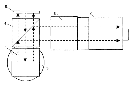
As shown in Figs.1, 2, 3, 4 and 5, the imaging apparatus for reference mark
measurement and inspection of the solder-paste printing, includes a first
reflector 1, a
second reflector 2, a low-angle ring light source 3, a first beamsplitter 4, a
second
beamsplitter 5, a first LED light source 6, a second LED light source 7, a
first imaging lens
8, a second imaging lens 10, a image sensor 9 and a second image sensor 10.
The two
stacked optical reflectors 1, 2 and the two stacked LED light sources 6, 7 are
5
CA 02594884 2007-07-26
correspondingly disposed on two opposite sides of the two stacked
beamsplitters 4, 5.
The two stacked imaging lens 8, 10 are disposed on another side of the
beamsplitters 4,
different from that of the optical reflectors and the light sources. The
optical axes of the
two stacked image sensors 8, 10 are orthogonal to that of the LED light
sources 6, 7. The
5 angles of the light-splitting planes of the two beamsplitters with respect
to the axes of the
two imaging lenses and the axes of the two light sources are both 45 . The
beams of light
from the first LED light source 6 and the second LED light source 7 are
refracted to the
first reflector 1 and the second reflector 2 by the first beamsplitter 4 and
the second
beamsplitter 5, respectively. Then, the beams of light are reflected to the
screen 13 and
the printed circuit board 14 by the first reflector 1 and the second reflector
2, respectively.
The ring light source 3 is disposed below the reflector 2, so as to provide
side illumination
for the printed circuit board 14. The beam of light reflected downwards by the
reflector 2
travels through the central hole of the ring light source 3 and irradiates on
the printed
circuit board 14. The reflected beams of light of the screen 13 are reflected
in an angle of
90 towards the first beamsplitter 4 by the first reflector 1. The reflected
beams of light of
the printed circuit board 14 travel through the central hole of the ring light
source 3 and
then irradiate onto the second reflector 2 below, by which the beams of light
are reflected
back to the second beamsplitter 5. The first reflector 1 and the second
reflector 2 are two
isosceles right angle prisms stacked together. In the present embodiment, the
first
reflector 1 and the second reflector 2 may be two light-splitting plates or a
right angle
prism with two reflection planes. The first beamsplitter 4 and the second
beamsplitter 5
are right angle prisms stacked together, or a cuboid beamsplitter, or one or
two
light-splitting plates. A part of the reflected light is refracted towards the
first LED light
source 6 and the second LED light source 7 by the first beamsplitter 4 and the
second
beamsplitter 5 respectively; the other part of the reflected light is
reflected in an angle of
90 by the first beamsplitter 4 and the second beamsplitter 5 into the first
imaging lens 8
and the second imaging lens 10, and then imaging is obtained on the first
image sensor 9
and the second image sensor 11. The first image sensor 9 and the second image
sensor
11 may be formed of analog CCD cameras or digital CCD cameras or CMOS cameras,
so
that the images are converted into analog signals or digital signals by the
image sensors
and transferred to computer for processing. In the whole imaging apparatus,
the two
stacked reflectors and the two stacked light sources are disposed on two
opposite sides
of the two stacked beamsplitters. The imaging apparatus forms a T-shaped
structure, in
which the upper light path and the lower light path are independent with
respect to each
6
CA 02594884 2007-07-26
other, and acquire the image of the screen and the image of the printed
circuit board,
respectively.
As shown in Fig. 6, in order to cooperate with the operation of the imaging
apparatus
according to the present invention, an image acquiring control and processing
device 16
and a positioning device 15 are further required. The image acquiring control
and
processing device 16 consists of a camera controller, an image acquiring card,
a
positioning controller, an image processing model, a general computer and a
memory.
The camera controller is connected to the first LED light source 6, the second
LED light
source 7, the first image sensor 9 and the second image sensor 11
respectively, and
controls the image acquiring of the first image sensor 9 and the second image
sensor 11.
The image acquiring card is connected to the video interfaces of the first
image sensor 9
and the second image sensor 11, and the image video signals are converted into
digital
signals. The positioning controller is connected to the positioning device 15
on which the
imaging apparatus 12 is mounted. When acquiring the images, according to the
given
coordinate information, the imaging apparatus 12 is conveyed to a designated
position
between the screen 13 and the printed circuit board 14. The imaging apparatus
12
simultaneously captures the image of the screen on the side facing the printed
circuit
board, and the image of the printed circuit board on the side facing the
screen. The image
acquiring process is automatically controlled and accomplished by program. The
acquired images and the processing results are stored on the memory.
When using the imaging apparatus of this embodiment, the light emitted from
the first
LED light source 6 and the second LED light source 7 is refracted towards the
first
reflector 1 and the second reflector 2 by the first beamsplitter 4 and the
second
beamsplitter 5. A beam of light is reflected upwards to the screen 13 by the
first reflector 1,
while a beam of light is reflected downwards by the second reflector 2 and
travels through
the central hole of the ring light source 3 and irradiates onto the printed
circuit board 11.
The ring light source 3 provides side illumination for the image acquiring of
the printed
circuit board. The beam of light reflected back from the screen 10 is
reflected towards the
first beamsplitter 4 by the first reflector 1; the beam of light reflected
back from the printed
circuit board 14 travels through the central hole of the ring light source 3
and irradiates
onto the second reflector 2, and then is reflected to the second beamsplitter
5. 50% of the
light reflected back by the first reflector 1 and the second reflector 2 is
refracted towards
the first LED light source 6 and the second LED light source 7 by the first
beamsplitter 4
7
CA 02594884 2007-07-26
and the second beamsplitter 5. The other 50% of the light is reflected in an
angle of 900
towards the first imaging lens 8 and the second imaging lens 10 by the first
beamsplitter 4
and the second beamsplitter 5, and finally the upper and lower paths of light
are imaged
on the first image sensor 9 and the second image sensor 10 separately.
When the apparatus according to the embodiment of the present invention is
used
for reference mark measurement, the images of reference marks on the printed
circuit
board 14 and the screen 13 are simultaneously acquired, and then inputted into
computer
after being converted into digital signals by the image acquiring card, and
the coordinates
of the two reference marks can be calculated, and then deviation analysis is
carried out,
so that the alignment in high speed and high precision can be obtained.
When the apparatus according to the embodiment of the present invention is
used
for the inspection of the solder paste printing, the images of the printed
circuit board 14
and the screen 13 can be simultaneously acquired, and then inputted into
computer after
being converted into digital signals by the image acquiring card, and the
digital signals
are compared with the information of standard model stored on the computer, so
that the
block of the screen and the quality of solder-paste printing of the printed
circuit board can
be inspected.
EMBODIMENT 2: A L-type Imaging apparatus with Two Lenses for Fully Automatic
Screen Printer
As shown in Fig. 7, the two stacked reflectors 1, 2 and the two stacked
imaging
lenses 8, 10 are disposed on two opposite sides of the two stacked
beamsplitters 4, 5,
and the two stacked LED light sources 6, 7 are disposed on another side of the
two
stacked beamsplitters 4, 5 different from that of the reflectors and the
imaging lenses, so
that the imaging apparatus forms a L-shaped structure: The other features of
the
embodiment 2 are the same as that of the embodiment 1 as described above. The
optical axes of the first imaging lens 8 and the second imaging lens 10 are
both
orthogonal to that of the first LED light source 6 and the second LED light
source 7. The
angles of the light-splitting planes of the two beamsplitters 4, 5 with
respect to the axes of
the two imaging lenses 8, 10 and the axes of the two LED light sources 6, 7
are both 45 .
The light emitted from the first LED light source 6 and the second LED light
source 7
is reflected in an angle of 90 by the first beamsplitter 4 and the second
beamsplitter 5
towards the first reflector 1 and the second reflector 2. Then, the beams of
light are
8
CA 02594884 2007-07-26
reflected towards the screen 13 and the printed circuit board 14 by the
reflectors 1, 2,
respectively. The ring light source 3 is disposed below the reflector 2, so as
to provide
side illumination for the printed circuit board 14. The beam of light
reflected downwards
by the reflector 2 travels through the central hole of the ring light source 3
and irradiates
onto the printed circuit board 14. The beam of light reflected by the screen
13 is reflected
in an angle of 900 towards the first beamsplitter 4 by the first reflector 1.
The beam of light
reflected by the printed circuit board 14 travels through the central hole of
the ring light
source 3 and then irradiates onto the second reflector 2 below, by which the
beam of light
is reflected back to the second beamsplitter 5. The first reflector 1 and the
second
reflector 2 are two isosceles right angle prisms stacked together. The
reflectors also may
be formed of two reflection mirror or a right angle prism with two reflection
planes. A part
of the reflected light from the screen 13 or the printed circuit board 14 is
reflected in an
angle of 90 by the first beamsplitter 4 and the second beamsplitter 5 towards
the first
LED light source 6 and the second LED light source 7; the other part of the
reflected light
is refracted into the first imaging lens 8 and the second imaging lens 10 by
the first
beamsplitter 4 and the second beamsplitter 5, and imaging is respectively
obtained on
the image sensor 9 and the image sensor 10. The images are converted by the
image
sensors into analog voltage signals or digital signals. The images are
transferred to
computer for processing.
The operation mode of the imaging apparatus according to this embodiment is
the
same as that of the embodiment 1.
The embodiments described above are only the preferred examples without
intention to limit the protection scope of the present invention. Therefore,
any
amendments to the structure according to the present invention as described in
the
specification or the drawings are within the protection scope of the present
invention.
9