Note: Descriptions are shown in the official language in which they were submitted.
CA 02595114 2007-06-07
Organic field effect transistor gate
The invention relates to an electronic device, in
particular an RFID transponder, comprising at least one
logic gate formed from organic field effect
transistors.
The simplest logic gate is the inverter, from which all
complex logic gates, such as, for example, ANDs, NANDs,
NORs and the like, can be formed by combination with
further inverters and/or further electronic components.
Organic logic gates comprising only one type of
semiconductor - p-type semiconductors are typically
involved - as active layer are susceptible to parameter
fluctuations of the individual devices. This can mean
that said circuits operate unreliably or do not operate
at all as soon as individual devices, such as
transistors, cannot adequately fulfill the
specifications determined by the circuit design on
account of deviations in the production process.
Moreover, a dissipative current, that is to say a
current that does not stem from the function of the
circuit, flows in these circuits based only on one type
of semiconductor, depending on the circuit concept
used, at least during half of the operating time. As a
result, the power consumption is significantly higher
than is actually necessary.
Such logic gates are unsuitable for RFID transponders
(RFID = Radio Frequency Identification), for example,
since the RFID transponders obtain their supply voltage
from a radiofrequency signal that is received by means
of a small antenna and then rectified. RFID
transponders are increasingly being employed for
providing merchandise or security documents with
information that can be read out electronically. They
are thus being employed for example as electronic bar
code for consumer goods, as luggage tag for identifying
luggage or as security element that is incorporated
CA 02595114 2007-06-07
_ 2 -
into the binding of a passport and stores
authentication information.
The document KLAUK, H. et al.: Pentacene Thin Film
Transistors and Inverter Circuits. In: IEDM Tech. Dig.,
December 1997, pp. 539-542, describes an inverter
comprising organic field effect transistors of
identical type, which is formed from a charging field
effect transistor and a switching field effect
transistor, which transistors are connected in series.
The production of the field effect transistors is
provided by thermal deposition of the organic
semiconductor material.
Combinations of different semiconductors for logic
gates are also known, but hitherto only organic
semiconductors have been combined with inorganic
semiconductors, for example described in the document
BONSE, M. et al.: Integrated a-Si:H/Pentacene
Inorganic/Organic Complementary Circuits. In: IEEE IEDM
98, 1998, pp. 249-252, or organic semiconductors have
been combined with organometallic semiconductors, as
reported in the document CRONE, B. K. et al,: Design
and fabrication of organic complementary circuits. In:
J. Appl. Phys.. Vol. 89, May 2001, pp. 5125-5132.
Thermal deposition of the organic semiconductor is
likewise provided as the production method for the
field effect transistors in both documents.
It is an ob j ect of the present invention to specify an
improved electronic device using field effect
transistors.
This object is achieved according to the invention by
forming an electronic device comprising at least one
logic gate, wherein the logic gate is formed from a
plurality of layers which are applied on a common
substrate, which comprise at least two electrode layers
at least one, in particular organic, semiconductor
CA 02595114 2007-06-07
- 3 -
layer applied from a liquid, and an insulator layer and
which are formed in such a way that the logic gate
comprises at least two differently constructed field
effect transistors.
In this case, the term liquid encompasses for example
suspensions, emulsions, other dispersions or else
solutions. Such liquids can be applied by printing
methods, for example, wherein parameters such as
viscosity, concentration, boiling point and surface
tension determine the printing behavior of the liquid.
Field effect transistors are understood hereinafter to
mean field effect transistors whose semiconductor
layers have essentially been applied from said liquids.
By forming two, in particular, organic, field effect
transistors which differ in terms of their construction
on a common carrier with at least one semiconductor
layer applied from liquid, it is possible to form logic
gates having properties which cannot be obtained
otherwise.
In this way, it is possible to realize faster logic
gates than by means of the previous embodiment with
only one semiconductor. Thus, to date it has been
conventional practice to construct circuits based on
only one type of semiconductor on a carrier, that is to
say that silicon-based ICs have only silicon-based
transistors. The invention makes it possible to
simplify the circuit design, to increase the switching
speed, to reduce the power consumption and/or to
increase the reliability. At the same time it is
therefore ensured that this type of logic gate can be
produced by means of fast and continuous production
methods, for example in a roll-to-roll printing method.
The logic gates according to the invention are
furthermore distinguished by greater insensitivity
toward production tolerances. A further advantage of
the logic gates according to the invention is their
CA 02595114 2007-06-07
- 4 -
lower power consumption by comparison with
conventional, in particulax organic, logic gates.
Therefore, the circuit layout no longer has to be
developed in a manner taking account of reserves, such
as, for example, by overdimensioning the individual
devices or by inserting redundant components.
The organic field effect transistor, referred to
hereinafter as OFET, is a field effect transistor
comprising at least thr=ee electrodes and an insulating
layer. The OFET is arranged on a carrier substrate,
which may be formed as a solid substrate or as a film,
for example as a polymer film. A layer composed of an
organic semiconductor forms a conductive channel, the
end sections of which are formed by a source electrode
and a drain electrode. The layer composed of an organic
semiconductor is applied from a liquid. The organic
semiconductors may be polymers dissolved in the liquid.
The liquid containing the polymers may also be a
suspension, emulsion or other dispersion.
The term polymer here expressly includes polymeric
material and/or oligomeric material and/or material
composed of "small molecules" and/or material composed
of "nanoparticles". Layers composed of nanoparticles
can be applied by means of a polymex suspension, for
example. Therefore, the polymer may also be a hybrid
material, for example in order to form an n-conducting
polymeric semiconductor. All types of substances with
the exception of the traditional semiconductors
(crystalline silicon or germanium) and the typical
metallic conductors are involved. A restriction in the
dogmatic sense to organic material within the meaning
of carbon chemistry is accordingly not intended.
Rather, silicones, for example, are also included.
Furthermore, the term is not intended to be restricted
with regard to the molecular size, but rather to
include "small molecules" or "nanoparticles", as
CA 02595114 2007-06-07
- 5 -
already explained above. Nanoparticles comprise
organometallic semiconductor-organic compounds
containing zinc oxide, for example, as non-organic
constituent. It may be provided that the semiconductor
layers are formed with different organic materials.
The conductive channel is covered with an insulation
layer, on which a gate electrode is arranged. The
conductivity of the channel can be altered by
application of a gate-source voltage UGs between gate
electrode and source electrode. The semiconductor layer
may be formed as a p-type conductor or as an n-type
conductor. The current conduction in a p-type conductor
is effected almost exclusively by defect electrons, and
the current conduction in an n-type conductor is
effected almost exclusively by electrons. The
prevailing charge carriers present in each case are
referred to as majority carriers. Even though p-type
doping is typical of organic semiconductors, it is
nevertheless possible to form the material with n-type
doping. Pentacene, polyalkylthiophene, etc. may be
provided as p-conducting semiconductors, and e.g.
soluble fullerene derivatives may be provided as
n-conducting semiconductors.
The majority carriers are densified by the formation of
an electric field in the insulation layer if a gate-
source voltage UGg of suitable polarity is applied, that
is to say a negative voltage in the case of p-type
conductors and a positive voltage in the case of n-type
conductors. The electrical resistance between the drain
electrode and the source electrode consequently
decreases. Upon application of a drain-source voltage
UGS, it is then possible for a larger current flow to
form between the source electrode and the drain
electrode than in the case of an open gate electrode. A
field effect transistor is therefore a controlled
resistor. The logic gate according to the invention,
through combination of two differently formed field
CA 02595114 2007-06-07
- 6 -
effect transistors, in particular OFETs, then avoids
the disadvantage of combinations of field effect
transistors of identical type, in particular OFETs, of
forming a dissipative current, i.e. exhibiting a
current flow when they are not driven.
Advantageous embodiments of the invention are presented
in the subclaims.
It is provided that the at least two different field
effect transistors have semiconductor layers which
differ in terms of their thickness. The formation of
the different thicknesses may be provided by means of
semiconductors formed in soluble fashion,
advantageously in a printing process. For this purpose,
in the case of organic semiconductors, provision may be
made for varying the polymer concentration of the
semiconductor. In this way, a layer thickness of the
organic semiconductor that is dependent on the polymer
concentration is formed after the evaporation of the
solvent.
It may also be provided that the semiconductor layers
of the field effect transistors are formed with
different conductivities. The conductivity of the, in
particular organic, semiconductor layer can be
decreased or increased for example by means of a
hydrazine treatment and/or by targeted oxidation. The
field effect transistor formed with such a
semiconductor material can thus be set in such a way
that its off currents are only approximately one order
of magnitude less than the on currents. The off current
is the current which flows in the field effect
transistor between source electrode and drain electrode
if no electrical potential is present at the gate
electrode. The on current is the current which flows in
the field effect transistor between source electrode
and drain electrode if an electrical potential is
present at the gate electrode, for example a negative
CA 02595114 2007-06-07
- 7 -
= potential if a field effect transistor with p-type
conduction is involved.
It is therefore advantageous to use differ-ent types of
semiconductors or to arrange a different combination of
semiconductors for forming an electronic functional
layer alongside one another, and thus to influence
properties such as charge mobility, switching speed and
power or switching behavior in a targeted manner.
It may also be provided that the field effect
transistors differ in the formation of the insulator
layer. They may have insulator layers having different
thicknesses and/or different materials. However, the
insulator layers of the at least two differently formed
field effect transistors may also differ in terms of
their permeability and thus influence the charge
carrier density that can be formed in the semiconductor
layers, or be formed as a dielectric for the capacitive
coupling of electrodes, for example for coupling the
gate electrode to the source or drain electrode of the
same field effect transistor.
The different areal structuring of the layers is
possible in a particularly cost-effective manner. This
is possible in a particularly simple manner in the case
of a printing method, such that in this case the
behavior of the field effect transistors can be
optimized according to the trial and error method
without specifically knowing the functional
dependencies. The two different field effect
transistors may be formed for example with different
channel widths and/or channel lengths. Strip-type
structures may preferably be provided. However,
arbitrarily contoured structures may also be provided,
for example for forming the electrodes of the field
effect transistors, such as the gate electrode. The
geometrical dimensions are dimensions in the m range,
for example channel widths of 30 m to 50 m, tending
CA 02595114 2007-06-07
- 8 -
toward even smaller dimensions in order to obtain high
switching speeds and low capacitances between the
electrodes. It is known from conventional silicon
technology that component capacitances cause high power
losses and therefore have a critical influence on
minimizing the power demand of the circuit.
In this way, it is also possible to form field effect
transistors having different switching capacitances,
for example in order to form different switching
behaviors.
Provision may be made for arranging the at least two
different field effect transistors alongside one
another or one above another. In this way, circuit
designs can be transferred particularly simply into
layouts and the number of plated-through holes, so-
called vias, for example, can be minimized. However,
the arrangement of the field effect transistors may
also be provided for functional reasons, for example in
order to form two field effect transistors having a
common gate electrode, in which case an arrangement of
the two field effect transistors one above another may
be particularly advantageous.
The field effect transistors may be arranged with
identical orientation or with different orientations.
It is provided that the at least two differently formed
field effect transistors may be arranged with bottom-
gate or top-gate orientation.
Provision may be made for varying the at least two
different field effect transistors in such a way that
they are formed with a different resistance
characteristic curve and/or a different switching
behavior. The resistance characteristic curve can be
altered for example by changing the thickness of the
semiconductor layer, in which case, by forming
particularly thin layers - for example in the case of
CA 02595114 2007-06-07
- 9 -
layers within the range of 5 nm to 30 nm - additional
effects can be set which cannot be observed given
thicker layers of the order of magnitude of 200 nm.
The at least two different field effect transistors may
be connected to one another in a parallel and/oz series
connection. It may be provided, for example, that two
differently formed field effect transistors, in
particular two OFETs, in series connection form the
load OFET and the switching OFET. However, it may also
be provided, for example, that load OFET and/or
switching OFET are formed by parallel or series
connection of two or more different OFETs. In this way,
a logic gate formed as an inverter may be formed for
example from four - preferably different - field effect
transistors. Such logic gates can be connected to form
a ring oscillator that can be used, in particular in
RFID transponders, as a logic circuit or oscillation
generator.
The solution according to the invention is not
restricted to the direct electrical coupling of the
field effect transistors. Rather, provision may be made
for capacitively coupling the field effect transistors
to one another, for example by enlarging a gate
electrode and a further electrode in such a way that
together with the insulation layer they form a
capacitor having a sufficient capacitance. Owing to the
possible very small layer thickness of the insulation
layer and, if appropriate, of further layers arranged
between the capacitively coupled electrodes,
comparatively high capacitance values can be formed
despite small electrode areas.
Provision may also be made for forming the different
field effect transistors with semiconductor layers of
different conduction types, that is to say with
p-conducting and n-conducting semiconductor layers.
Even though p-conducting semiconductor layers are still
CA 02595114 2007-06-07
- 10 -
preferred for forming OFETs, applying an n-conducting
layer is nevertheless not more difficult than applying
a p-conducting layer. In this way, p-n junctions can
also be formed between the two adjoining layers.
The logic gate according to the invention is formed in
such a way that it can essentially be produced by
printing (e.g. by intaglio printing, screen printing,
pad printing) and/or blade coating. The entire
construction is therefore directed at forming layers
which form the logic gate in their interaction and
which can be structured by means of the two methods
mentioned. Tried and tested equipment is available for
this, as is provided for example for the producing of
optical security elements. The gates according to the
invention can therefore be produced on the same
installations.
The differing formation of the field effect transistors
can be achieved particularly well if the layers of the
at least two different field effect transistors, in
particular the OFETs, are formed as printable
semiconducting polymers and/or printable insulating
polymers and/or conductive printing inks and/or
metallic layers.
The thickness of the soluble polymeric layer can be set
in a particularly simple manner through its solvent
proportion. However, it may also be provided that the
thickness of the soluble organic layer can be set
through its application quantity, for example if the
application of the layer by pad printing or by blade
coating is provided. Thicker layers can preferably be
formed in this way. As an alternative to this, the
layered construction of a layer may be provided. If, by
way of example, the at least two different field effect
transistors have a semiconductor layer of identical
material with different thicknesses, the thin layer of
one field effect transistor can be applied in a first
CA 02595114 2007-06-07
- 11 -
pass and this basic layer can be reinforced for the
other field effect transistor in one or more further
passes. For this purpose, provision may be made for
applying the layers with different solvent proportions,
i.e. the basic layer with a high solvent proportion and
the further layer or the further layers with a low
solvent proportion.
It may preferably be provided that the electronic
device produced in the manner described above is formed
by a multilayer flexible film body. The flexibility of
the electronic device can make it particularly
resistant, in particular if it is applied to a flexible
support. The organic electronic devices formed
according to the invention as multilayer flexible film
bodies are, moreover, completely insensitive to impact
loads and, in contrast to devices applied on rigid
substrates, can be used in applications in which
printed circuit boards are provided which nestle
against the contour of the electronic apparatus. There
is an increasing trend toward providing these for
apparatuses having irregularly formed contours, such as
mobile phones and electronic cameras.
Provision may be made for forming security elements,
merchandise labels or tickets with one or a plurality
of logic gates according to the invention.
The invention will now be explained in more detail with
reference to the drawings, in which:
Figures 1 and 2 show schematic sectional
illustrations of a first exemplary
embodiment;
Figures 3a and 3b show basic circuit diagsams of the
first exemplary embodiments in
figures 1 and 2;
CA 02595114 2007-06-07
- 12 -
Figure 4 shows a schematic sectional
illustration of a second exemplary
embodiment;
Figure 5 shows a schematic sectional
illustration of a third exemplary
embodiment;
Figure 6 shows a schematic sectional
illustration of a fourth exemplary
embodiment;
Figure 7 shows a basic circuit diagram of the
exemplary embodiments in figures 5
and 6;
Figure 8 shows a schematic current-voltage
diagram of a logic gate;
Figure 9a shows a first schematic output
characteristic curve diagram of a
logic gate comprising differently
formed organic field effect
transistors;
Figure 9b shows a second schematic output
characteristic curve diagram of a
logic gate comprising differently
formed organic field effect
transistors.
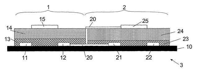
Figures 1 and 2 in each case show a schematic sectional
illustration of a logic gate 3, formed from two
differently formed organic field effect transistors 1,
2, referred to hereinafter as OFET, which are arranged
on a substrate 10. However, field effect transistors
which are not formed, or not completely formed, from
organic semiconductor material may also be involved in
this case. The substrate may be for example a laminar
CA 02595114 2007-06-07
- 13 -
substrate or a film. The film is preferably a plastic
film having a thickness of 6 m to 200 m, preferably
having a thickness of 19 pm to 100 m, preferably
formed as a polyester film.
The first OFET 1 is formed from a first semiconductor
layer 13 with a source electrode 11 and a drain
electrode 12. An insulator layer 14 is arranged on the
semiconductor layer 13 with a gate electrode 15
arranged on said insulator layer.
These layers can be applied in an already partially
structured manner, or in a manner structured in
patterned fashion, by means of a printing method for
example. For this purpose, provision is made for
applying in particular the semiconductor layer from a
liquid. In this case, the term liquid encompasses for
example suspensions, emulsions, other dispersions or
else solutions. For preparing solutions, the organic
materials provided for the layers are formed as soluble
polymers, where the term polymer here, as already
described further above, also includes oligometers and
"small molecules" and nanoparticles. The organic
semiconductor may be for example pentacene. A plurality
of parameters of the liquid can be varied:
- the viscosity of the liquid, it determines the
printing behavior;
- the polymer concentration of the mixture ready for
printing, it determines the layer thickness;
- the boiling point of the liquid, it determines which
printing method can be used;
- the surface tension of the mixture ready for
printing, it determines the wettability of the
carrier substrate or other layers.
Provision may also be made, as described in detail
further above, for forming the layers with a variable
layer thickness by means of repeatedly successive
printing.
CA 02595114 2007-06-07
- 14 -
Provision may also be made for applying to the
substrate 10 a curable resist and structuring the
latter prior to curing in such a way as to form
depressions into which, by way of example,
semiconductor layers are introduced by blade coating.
Such method steps may be provided in order to combine
for example optical security elements produced using
curable resist layers with the logic gates according to
the invention.
The electrodes 11, 12 and 15 preferably comprise a
conductive metallization, preferably composed of gold
or silver. However, provision may also be made for
forming the electrodes 11, 12 and 15 from an inorganic
electrically conductive material, for example from
indium tin oxide, or from a conductive polymer, for
example polyaniline or polypyrrole.
The electrodes 11, 12 and 15 may in this case be
applied in a manner already partially structured in
patterned fashion to the substrate 10 or to the organic
insulator layer 14, or another layer provided in the
production method, for example by means of a printing
method (intaglio printing, screen printing, pad
printing) or by means of a coating method. However, it
is also possible for the electrode layer to be applied
to the substrate 10, or another layer provided in the
production method, over the whole area or over a
partial area and then to be partially removed again and
thus structured by means of an exposure and etching
method or by ablation, for example by means of a pulsed
laser.
The electrodes 11, 12 and 15 are structures in the m
range. The gate electrode 15, for example, may have a
width of 50 m to 1000 m and a length of 50 m to
1000 m. The thickness of such an electrode may be
0.2 pm or less.
CA 02595114 2007-06-07
- 15 -
The second OFET 2 is formed from a first organic
semiconductor layer 23 with a source electrode 21 and a
drain electrode 22. An organic insulator layer 24 is
arranged on the organic semiconductor layer 23 of the
gate electrode 25 arranged on said insulator layer.
In figure 1, the drain electrode 12 of the first OFET I
is connected to the source electrode 21 of the second
OFET 2 and to the gate electrode 25 of the second OFET
2 by means of the electrically conductive connecting
layers 20.
Furthermore, it is also possible for the gate electrode
25 to be connected to the drain electrode 22 instead of
to the source electrode 21.
In figure 2, the gate electrode 15 of the first OFET 1
and the gate electrode 25 of the second OFET 2 and also
the drain electrode 12 of the first OFET 1 and the
drain electrode 22 of the second OFET 2 are connected
by means of electrically conductive connecting layers
20.
In these exemplary embodiments in accordance with
figures 1 and 2, the two OFETs 1, 2 lie alongside one
another with identical orientation, that is to say
that, by way of example, the gate electrodes 15, 25 are
arranged in one plane. In the case illustrated, the
top-gate orientation is chosen for both OFETs, in other
words the two gate electrodes 15, 25 are formed as the
topmost layer. However, it may also be provided that
the bottom-gate orientation is chosen for both OFETs,
in which orientation the two gate electrodes 15, 25 are
arranged directly on the substrate 10.
As can be discerned in figure 1 and figure 2, the
organic semiconductor layers 13, 23 determining the
electrical properties of the two OFETs 1, 2 and/or the
CA 02595114 2007-06-07
- 16 -
organic insulator layers 14, 24 can be formed with
different layer thicknesses, both OFETs 1, 2 being
formed with the same overall layer thickness in the
exemplary embodiment illustrated. It may preferably be
provided that the organic semiconductor layers 13, 23
are applied in strips. In order to form different
electrical behaviors of the two OFETs 1, 2, provision
may be made for forming differently the thickness
and/or the channel length, i.e. the distance between
the source electrode 11, 21 and the drain electrode 12,
22, and/or the material of the organic semiconductor
layers 13, 23 of the two OFETs 1, 2. The material of
the organic semiconductor layers 13, 23 may for example
be doped identically or to different extents. The
semiconductors layers 13, 23 may be formed as p-type
conductors or as n-type conductors. The current
conduction in a p-type conductor is effected almost
exclusively by defect electrons, and the current
conduction in an n-type conductor is effected almost
exclusively by electrons. The prevailing charge
carriers present in each case are referred to as
majority carriers. Even though p-type doping is typical
of organic semiconductors, it is nevertheless possible
to form the material with n-type doping. Thus, by way
of example the p-conducting semiconductor may be formed
from pentacene, polythiophene, and the n-conducting
semiconductor may be formed for example from
polyphenylenevinylene derivatives or fullerene
derivatives.
If both organic semiconductor layers 13, 23 have
different majority charge carriers, a logic gate 3
comprising semiconductor layers 13, 23 having
complementary conductivities is formed. Such a gate is
illustrated in figure 2, for example, and is
distinguished by the fact that a respective one of the
two field effect transistors permits no current flow
between source and drain as long as the input voltage
of the logic gate does not change, that is to say that
CA 02595114 2007-06-07
- 17 -
. the gate assumes one of its two switching states. A
dissipative shunt current through the gate flows only
during the switching operation. Consequently, logic
circuits comprising the logic gates according to the
invention have a significantly lower current
consumption than logic circuits which are formed from
identical OFETs. This is particularly advantageous if
only current sources having low loading capacity are
available, as is the case for example in RFID
transponders that obtain their energy from a rectified
antenna signal stored in a capacitor.
Figures 3a and 3b show the two basic circuits that can
be produced with the first exemplary embodiment in
figures 1 and 2. The positions in figures 1 and 2 have
been maintained for the sake of better illustration.
Figure 3a shows a logic gate 3, formed from two
different OFETs 1 and 2 having semiconductor layers of
the same conduction type. The two OFETs 1, 2 are
connected in series, the drain electrode 12 of the
first OFET 1 being connected to the source electrode 21
of the second OFET 2. The gate electrode 15 of the OFET
1 forms the input of the logic gate, and the gate
electrode 25 of the OFET 2 is connected to the source
electrode 21 of the OFET 2. The logic gate may be an
inverter comprising load OFET 2 and switching OFET 1.
Figure 3b shows a logic gate 3, formed from two
different OFETs 1 and 2 of differing doping types. Such
a logic gate, as described further above, is formed
with a lower power consumption than an OFET logic gate
according to the prior art. The two OFETs 1 and 2 are
connected in series, the drain electrode 12 of the
first OFET 1 being connected to the drain electrode 22
of the second OFET 2. The gate electrodes 15 and 25 of
the two OFETs are connected to one another and
represent the input of the logic gate.
CA 02595114 2007-06-07
- 18 -
Figure 4 then shows a second exemplary embodiment, in
which the two OFETs 1, 2 are arranged alongside one
another with different orientations on the substrate
10. In this case, the first OFET 1 is arranged in such
a way that the source electrode 11 and the drain
electrode 12 are arranged directly on the substrate 10
and are successively followed by the semiconductor
layer 13, the insulator layer 14, the second
semiconductor layer 23, which is different from the
first semiconductor layer, and the gate electrode 15.
Such an orientation of the OFET is referred to as top-
gate orientation. The second OFET 2 is arranged, then,
in such a way that the gate electrode 25 is arranged on
the substrate 10 and the source electrode 21 and the
drain electrode 22 are arranged such that they lie at
the top on the OFET 2. Such an orientation is referred
to as bottom-gate orientation. The gate electrode 25 of
the OFET 2 is connected to the source contact 21 of
OFET 2 and the drain contact 12 of OFET 1 by means of
the electrically conductive connecting layer 20, which,
in this exemplary embodiment, is formed in sections as
a plated-through hole running perpendicular to the
substrate 10.
In the exemplary embodiment illustrated it may
preferably be provided that the electrodes arranged in
a plane in each case are formed from identical
material, for example from a conductive printing ink or
from a metal layer applied by sputtering,
electroplating or vapor deposition. However, it may
also be provided that they are formed from different
materials in each case, preferably if this is
associated with an advantageous functional effect.
In the exemplary embodiment illustrated in figure 4,
the semiconductor layers 13 and 23 and the insulator
layer 14 are formed as layers common to both the OFETs
1, 2. In this case, for OFET 1 exclusively the
semiconductor layer 13 produces the connection between
CA 02595114 2007-06-07
- 19 -
source 11 and drain 12. The conductive channel
necessary for the function of the OFET 1 is formed in
said semiconductor layer 13 at the interface with the
insulator layer 14. For OFET 2, by contrast,
exclusively the semiconductor layer 23 produces the
connection between source 21 and drain 22. As can
zeadily be discerned in figure 4, the OFETs 1, 2 are
formed with different geometries, here in particular
with different channel lengths. However, it may also be
provided that both OFETs 1, 2 are formed with different
semiconductor layers and/or insulator layers.
The basic circuits that can be formed with the second
exemplary embodiment illustrated in figure 4 correspond
to the basic circuits illustrated in figures 2a and 2b.
It may be provided that the two OFETs 1, 2 are
connected to one another by further connecting lines
(not illustrated in figures 2a, 2b) in such a way that
they are interconnected or connected to other
components in parallel or series connection.
The basic circuit diagram of the exemplary embodiment
illustrated in figure 4, in which the two OFETs 1, 2
are formed with common semiconductor layers that may be
formed as p-type conductors or as n-type conductors, is
shown in figure 2a.
Figure 2b shows the basic circuit diagram of a modified
exemplary embodiment in comparison with figure 4,
wherein the two semiconductor layers of the OFETs 1, 2
are formed differently and with complementary
conduction types. This case emerges from the drawing in
figure 4 by the depicted connection 20 exclusively
connecting the two gate contacts 15 and 25, while a
connection of identical type to the connection 20 is
additionally placed between drain contact 22 of OFET 2
and drain 12 of OFET 1.
CA 02595114 2007-06-07
- 20 -
Figure 5 shows a third exemplary embodiment, in which
the two OFETs 1, 2 are arranged in a manner lying one
above the other on the substrate 10 and are formed with
a common gate electrode 15. The source electrode 11 and
the drain electrode 12 of the first OFET 1 are
therefore arranged in a manner lying directly on the
substrate 10, and the source electrode 21 and the drain
electrode 22 are formed as topmost layer of the OFETs
1, 2 lying one on top of another. The logic gate formed
from the two OFETs 1, 2 is therefore constructed from a
total of 7 layers. In this case, layers having an
identical function may be constructed identically or
differently, it being provided that at least one of the
layers of a layer pair is formed differently. By way of
example, it may be provided that the semiconductor
layers 13, 23 are formed with different conduction
types (p-type conduction, n-type conduction) and/or
different geometries.
The two drain electrodes 12, 22 are connected to the
electrical interconnect 20 formed as plated-through
hole.
Figure 6 then shows a fourth exemplary embodiment, in
which the two OFETs 1, 2 are arranged in a manner lying
one above the other on the substrate 10 and are formed
with a common gate electrode 15, but both OFETs 1, 2
are arranged with identical orientation on the
substrate. In this case, the common gate electrode 15
is formed as topmost layer of the logic gate, which is
formed with 7 layers like the logic gate illustrated in
figure 5.
In the example illustrated, the source electrode 11 and
the drain electrode 12 of the first OFET 1 are arranged
as a first layer directly on the substrate 10 and are
covered by the semiconductor layer 13. The insulator
layer 14 is arranged on the semiconductor layer 13. The
second OFET 2 is then arranged with the same
CA 02595114 2007-06-07
- 21 -
orientation and the same layer sequence on the OFET 1,
that is to say that the source electrode 21 and the
drain electrode 22 are applied on the insulator layer
14 and are covered with the semiconductor layer 23, on
which the insulator layer 24 of the OFET 2 is applied.
The common gate electrode 15 is arranged thereon as a
final layer.
The two drain electrodes 12, 22 are connected by means
of the electrically conductive connecting layer 20,
which is formed as a plated-through hole.
However, it may also be provided that the arrangement
described above is formed in such a way that the common
gate electrode 15 is formed as bottom-most layer lying
directly on the substrate 10.
Owing to the above-described possibility of rotating
the arrangement of the layers forming the logic gate
through 180 , a particularly advantageous topology of
interconnected logic gates or other components can be
formed and in this way it is possible for example to
avoid or minimize the number of plated-through holes
for connecting the logic gates or components.
Figure 7 then shows the basic circuit that is possible
with the exemplary embodiments illustrated in figures 5
and 6.
The two OFETs 1, 2 form in each case a logic gate
comprising a common gate electrode 15 and drain
electrodes 12, 22 that are conductively connected to
one another. The two source electrodes 11 and 21 form
further terminals of the logic gate for supply voltage
and ground. The logic gate illustrated in figure 7 can
be formed differently with regard to the conduction
type of the semiconductor layers. Semiconductor layers
of identical conduction type or semiconductor layers
CA 02595114 2007-06-07
- 22 -
formed with complementary conduction types may be
involved in this case.
Figure 8 then shows an example of a current-voltage
diagram of a logic gate with OFET that is formed as an
inverter. A logic gate comprising an OFET can form an
inverter in which the source electrode is connected to
the circuit ground, the gate electrode forms the input
of the inverter and the drain electrode forms the
output of the inverter and is connected to the supply
voltage via a load resistor. As soon as the gate
electrode is then connected to an input voltage, a
current flow forms between source electrode and drain
electrode, whereby the channel resistance of the OFET
is reduced to an extent such that the drain electrode
has approximately zero potential. As soon as the input
voltage at the gate electrode is then zero, the channel
resistance of the OFET rises to such a great extent
that the drain electrode has approximately the
potential of the supply voltage. In this way,
therefore, the input voltage is transformed into an
inverted output voltage, that is to say that the input
signal of the inverter is inverted. In practice, the
load resistor of the inverter is likewise formed as an
OFET. For better differentiation, this OFET is referred
to as the load OFET and the OFET that effects switching
is referred to as the switching OFET.
The current-voltage diagram in figure 8 shows the
dependence between the forward current ID through
switching OFET or load resistor and the output voltage
Uout= In this case, 80e denotes the on characteristic
curve and 80a denotes the off characteristic curve of
the switching OFET, and 80w denotes the resistance
characteristic curve of the load resistor. The points
of intersection 82e and 82a of the resistance
characteristic curve 80w with the on characteristic
curve 80e and with the off characteristic curve 80a
denote the switching points of the inverter, which are
CA 02595114 2007-06-07
-23-
spaced apart from one another by a voltage swing 82h of
the output voltage Uoõt. A charge-reversal current flows
during each changeover operation of the inverter, the
magnitude of said current being symbolized by the
hatched areas 84e and 84a. Fast logic gates which can
be switched reliably and well at the same time are
distinguished by the schematically illustrated
properties in figure 8 of the large voltage swing 82h
and the charge-reversal currents 84e and 84a
approximately identical in magnitude.
Figure 9a qualitatively illustrates a first profile of
the output voltage Uouti of the inverter as a function of
the input voltage Uin. In this case, the curve 82k is to
be assigned to the inverter from figure 8. The position
of the off level 82e is directly dependent on the
position of the curves 80e and 80w in figure 8. By
means of the embodiment according to the invention of
the logic gates comprising at least two different OFETs
1, 2, as illustrated in figure 2b, for example, the
advantageous characteristic curve 86k illustrated in
figure 9a can be formed for example by forming the two
OFETs with semiconductors layers 13, 23 having
different thicknesses. The advantage resides in the
larger voltage swing 86h that results from this in
comparison with 82h.
Figure 9b shows a second profile of the output voltage
Uoõt of the inverter as a function of the input voltage
Uiõ in a qualitative illustration. The voltage swing 86h
is now enlarged again because the characteristic curve
86h includes the output voltage Uoõt = 0. Such an
inverter is formed with a particularly low power loss.
The embodiment of the logic gates according to the
invention comprising different field effect transistors
which can be produced by layer-by-layer printing and/or
blade coating enables the cost-effective mass
production of the logic gates according to the
CA 02595114 2007-06-07
- 24 -
invention. The printing methods have reached a state
such that extremely fine structures can be formed in
the individual layers which can only be formed with a
high outlay using other methods.