Note: Descriptions are shown in the official language in which they were submitted.
CA 02595151 2007-07-27
BALANCING CIRCUIT FOR A METAL DETECTOR
BACKGROUND
[0001] The invention relates to a balancing circuit for a metal detector.
Known
metal detectors include an oscillator (or transmit) coil and two detector (or
receive)
coils. The receive coils are typically positioned on either side of the
oscillator coil
and substantially equidistant therefrom. The oscillator coil is provided with
an
oscillatory signal that is inductively coupled to the detector coils. Metal
passing
through the coils causes an imbalance in the inductively coupled signals,
which can
be used to detect the presence of the metal.
[0002] To operate properly, the inductively coupled signals should be balanced
such that the signals produced by each receive coil are the same when metal is
not
present. Due to variances in tolerances, aging of materials, etc., it is
necessary to
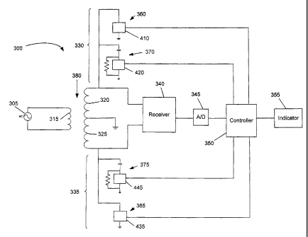
provide a means of balancing the inductively coupled signals when no metal is
present.
SUMMARY
[0003] In one embodiment, the invention provides a metal detector including
an
oscillating power source, a transmit coil connected to the oscillating power
source,
first and second receive coils inductively coupled to the transmit coil, a
first amplitude
balancing circuit connected to one of the first receive coil and the second
receive
coil, and a first phase balancing circuit connected to one of the first
receive coil and
the second receive coil, the first phase balancing circuit including a first
capacitor
and a first variable resistor.
[0004] In another embodiment, the invention provides a method of balancing
a
metal detector. The metal detector includes a transmit coil, first and second
receive
coils inductively coupled to the transmit coil, a differential circuit coupled
to the first
and second receive coils, a first amplitude balancing circuit coupled to one
of the first
receive coil and the second receive coil and including a first variable
resistor, and a
first phase balancing circuit coupled to one of the first receive coil and the
second
receive coil and including a capacitor. The method includes detecting a
difference
between a signal from the first receive coil and a signal from the second
receive coil
1
CA 02595151 2014-11-03
67363-1591
when there is no material in the metal detector, adjusting the first variable
resistor to
reduce the difference, adjusting the second variable resistor to reduce the
difference,
and repeating adjustment of the first and second variable resistors to reduce
the
difference.
[0005] In another embodiment the invention provides a signal adjuster for
an
inductor. The signal adjuster includes, an amplitude adjuster configured to
provide a
resistance between a lead of the inductor and ground, and a phase adjuster
configured to provide a capacitance and a variable resistance between a lead
of the
inductor and ground. The variable resistance is configured to adjust a phase
of a
signal generated by the inductor.
[0005a] According to one aspect of the present invention, there is
provided a
metal detector, comprising: an oscillating power source; a transmit coil
connected to
the oscillating power source; first and second receive coils inductively
coupled to the
transmit coil; a first amplitude balancing circuit connected to the first
receive coil; a
first phase balancing circuit connected to the first receive coil, the first
phase
balancing circuit including a first capacitor and a first variable resistor; a
second
amplitude balancing circuit connected to the second receive coil; and a second
phase
balancing circuit connected to the second receive coil, the second phase
balancing
circuit including a second capacitor and a second variable resistor.
[0005b] According to another aspect of the present invention, there is
provided
a method of balancing a metal detector having a transmit coil, first and
second
receive coils inductively coupled to the transmit coil, a differential circuit
coupled to
the first and second receive coils, a first amplitude balancing circuit
coupled to one of
the first receive coil and the second receive coil and including a first
variable resistor,
and a first phase balancing circuit coupled to one of the first receive coil
and the
second receive coil and including a capacitor and a second variable resistor,
the
method comprising: detecting a difference between a signal from the first
receive coil
and a signal from the second receive coil when there is no material in the
metal
detector; adjusting the first variable resistor to reduce the difference;
adjusting the
2
CA 02595151 2014-11-03
67363-1591
second variable resistor to reduce the difference; and repeating adjustment of
the first
and second variable resistors to reduce the difference.
[0005c] According to another aspect of the present invention, there is
provided
a metal detector, comprising: an oscillating power source; a transmit coil
connected
to the oscillating power source; first and second receive coils inductively
coupled to
the transmit coil; a first amplitude balancing circuit connected to one of the
first
receive coil and the second receive coil; and a first phase balancing circuit
connected
to one of the first receive coil and the second receive coil, the first phase
balancing
circuit including a first capacitor, a fixed resistor, and a first variable
resistor, wherein
the first capacitor and the first variable resistor are connected in series,
and the fixed
resistor is connected across the first variable resistor, wherein the first
variable
resistor is also connected to ground, and the first capacitor is also
connected to the
first receive coil.
[0006] Other aspects of the invention will become apparent by
consideration of
the detailed description and accompanying drawings.
BRIEF DESCRIPTION OF THE DRAWINGS
[0007] Fig. 1 is a schematic representation of a prior art metal
detector.
[0008] Fig. 2 is a schematic diagram of a construction of a balancing
circuit
according to the invention.
[0009] Fig. 3 is a partial schematic diagram, partial block diagram of a
construction of a metal detector according to the invention.
[0010] Fig. 4 is a flow chart of a first embodiment of a process for
balancing
the metal detector of Fig. 3.
[0011] Figs. 5A and 5B are a flow chart of a second embodiment of a
process
for balancing the metal detector of Fig. 3.
2a
CA 02595151 2014-11-03
67363-1591
DETAILED DESCRIPTION
[0012] Before any embodiments of the invention are explained in
detail, it is to
be understood that the invention is not limited in its application to the
details of
construction and the arrangement of components set forth in the following
description
or illustrated in the following drawings. The invention is capable of other
embodiments and of being practiced or of being carried out in various ways.
Also, it
2b
CA 02595151 2007-07-27
is to be understood that the phraseology and terminology used herein is for
the
purpose of description and should not be regarded as limiting. The use of
"including," "comprising," or "having" and variations thereof herein is meant
to
encompass the items listed thereafter and equivalents thereof as well as
additional
items. Unless specified or limited otherwise, the terms "mounted,"
"connected,"
"supported," and "coupled" and variations thereof are used broadly and
encompass
both direct and indirect mountings, connections, supports, and couplings.
Further,
"connected" and "coupled" are not restricted to physical or mechanical
connections
or couplings.
[0013] In addition, it should be understood that embodiments of the
invention
include hardware, software, and electronic components or modules that, for
purposes of discussion, may be illustrated and described as if the majority of
the
components were implemented solely in hardware. However, one of ordinary skill
in
the art, and based on a reading of this detailed description, would recognize
that, in
at least one embodiment, the electronic based aspects of the invention may be
implemented in software. Similarly, some embodiments of the present invention
described herein operate utilizing software. One of ordinary skill in the art,
and
based on a reading of this detailed description, would recognize that, in at
least one
embodiment, such embodiments could instead operate without software, instead
utilizing electronic circuitry and other hardware configured to perform the
same
functions. As such, it should be noted that any number and combination of
hardware-based devices, software-based devices, and structural components may
be utilized to implement the various embodiments of the present invention.
Also,
although various components of the present invention are described and
illustrated
herein as being defined by modules, it will be appreciated that the modules
described and illustrated herein can be configured in a significantly
different manner,
can be defined by one or more other modules performing additional tasks,
and/or
can be defined by fewer modules.
[0014] Fig. 1 schematically illustrates a construction of a prior art metal
detector
100. The metal detector 100 includes a passageway 105. A transmit coil 110 is
centrally positioned around the passageway 105. A first receive coil 115 and a
second receive coil 120 are positioned around the passageway 105 on opposite
3
CA 02595151 2007-07-27
sides of the transmit coil 110, substantially equidistant from the transmit
coil 110. A
first lead 125 of the first receive coil 115 and a first lead 130 of the
second receive
coil 120 are connected to ground. A second lead 135 of the first receive coil
115 and
a second lead 140 of the second receive coil 120 are connected to a
differential
circuit 145.
[0015] During operation of the metal detector 100, an oscillatory signal
150 (e.g.
an AC signal) is supplied to the transmit coil 110. The transmit coil 110
transmits a
signal, based on the oscillatory signal. The first receive coil 115 and the
second
receive coil 120 receive, via inductive coupling, the signal transmitted by
the transmit
coil 110. The first and second receive coils 115 and 120 each generates an
output
signal based on the signals they receive from the transmit coil 110. When
there is
no material, particularly no metallic material, in the passageway 105 (i.e.,
the
passageway 105 is empty), the signals received by, and output by, the first
and
second receive coils 115 and 120 should be substantially equivalent. The
differential
circuit 145 compares the output of the first receive coil 115 to the output of
the
second receive coil 120, and outputs a signal indicative of a difference in
the signals.
In the case, where there is no material in the passageway 105, the signals
should be
substantially equivalent, and the differential circuit 145 outputs a signal
with a zero or
near zero signal (e.g, a zero amplitude analog signal or a digital zero
value).
[0016] When a non-metal material (e.g., a food product) enters the passageway
105, the signals received by the first receive coil 115 and the second receive
coil 120
differ. The amplitude of these signals can differ significantly but the phase
angles of
the signals will generally be different than the phase angle generated by a
metal.
Therefore, the outputs of the first receive coil 115 and the second receive
coil 120,
amplitude and phase angle, will differ. The differential circuit 145 then
outputs a
signal (e.g., analog or digital) indicative of the difference between the
first receive
coil 115 output and the second receive coil 120 output.
[0017] When a piece of metal (ferrous or non-ferrous) enters the passageway
105, the metal distorts the signal transmitted by the transmit coil 110, and
therefore,
the signals received by the first receive coil 115 and the second receive coil
120.
The distortion is greater nearer the metal. Therefore, the receive coil nearer
the
metal receives a signal having a greater distortion than the receive coil that
is farther
4
CA 02595151 2007-07-27
away from the metal. Accordingly, the outputs of the first receive coil 115
and the
second receive coil 120 can differ relatively significantly when metal is
present in the
passageway 105. The differential circuit 145 receives the different signals
from the
first receive coil 115 and the second receive coil 120 and generates an output
(e.g.,
analog or digital) indicative of the difference. The metal detector 100
receives the
relatively large output of the differential circuit 145 and detects the
presence of metal
in the passageway 105, taking appropriate action (e.g., sounding an alarm,
stopping
a conveyor, etc.).
[0018] The signals received by, and output by, the first receive coil 115
and the
second receive coil 120, should be equivalent when there is no material in the
passageway 105. Thus, the differential circuit 145 should output a zero signal
when
there is no material in the passageway 105. However, differences in the
signals
output by the first and second receive coils 115 and 120 can occur, even when
there
is no material in the passageway 105. For example, variances in the tolerances
of
the first receive coil 115 and the second receive coil 120, as well as in
manufacturing
the metal detector 100 (e.g., the positioning of the receive coils 115 and 120
relative
to the transmit coil 110), can result in differences in the signals received
by, and
output by, the receive coils 115 and 120. In addition, changes in temperature
can
also result in differences in the signals received by, and output by, the
receive coils
115 and 120.
[0019] The signals output by the receive coils include two components that
should match in order for the differential circuit 145 to output a relatively
zero signal.
The components are (1) the amplitudes of the signals and (2) the phases of the
signals. Reducing and/or removing the variations in the amplitude and/or phase
of
the outputs of the first receive coil 115 and/or the second receive coil 120,
when no
material is present in the passageway 105, improves the ability of the metal
detector
100 to detect when metal is actually present in the passageway 105.
[0020] A balancing circuit can be used to adjust the outputs of the first
receive coil
115 and the second receive coil 120, such that the amplitude and phase of the
output signals match when there is no material in the passageway 105. Fig. 2
illustrates a construction of a balancing circuit 200. The balancing circuit
200
includes an amplitude balancing circuit 205 and a phase balancing circuit 210.
The
CA 02595151 2007-07-27
amplitude balancing circuit 205 includes a variable resistor 215 (e.g., a 0-
20k
model AD5262 manufactured by Analog Devices) having a wiper 220 connected to a
receive coil 225 and a second lead 230 connected to ground.
[0021] The phase balancing circuit 210 includes a capacitor 235 (e.g., 2 to
20
nanofarad), a variable resistor 240 (e.g., a 0-20k 0 model AD5262 manufactured
by
Analog Devices), and a fixed resistor 245 (e.g., 100 0). A first lead 250 of
the
capacitor 235 is connected to the receive coil 225. A second lead 255 of the
capacitor 235 is connected to a wiper 260 of the variable resistor 240. A
second
lead 265 of the variable resistor 240 is connected to ground. The fixed
resistor 245
is connected across the variable resistor 240.
[0022] Fig. 3 illustrates a construction of a metal detector 300 embodying
the
present invention. The metal detector 300 includes an oscillatory power source
305,
a transmit coil 315, a first receive coil 320, a second receive coil 325, a
first
balancing circuit 330, a second balancing circuit 335, a receiver circuit 340,
an
analog-to-digital (ND) converter 345, a controller 350, and an indicator 355.
[0023] The oscillatory power source 305 provides an oscillatory signal
(e.g., an
AC signal) to the transmit coil. The transmit coil 315 transmits a signal
which is
received by the first receive coil 320 and the second receive coil 325. The
first
receive coil 320 and the second receive coil 325 provide output signals, to
the
receive circuit 340, based on the signals they receive from the transmit coil
315. The
receive circuit 340 amplifies any imbalance in the signals received from the
first
receive coil 320 and the second receive coil 325. The amplified differential
signal is
provided to the ND converter 345 where it is converted into a digital value
indicative
of the amplitude of the amplified differential signal. The digital value is
then provided
to the controller 350, which is also connected to the indicator 355, and the
first and
second balancing circuits 330 and 335. The controller 350 reduces and/or
removes
differences between the output signals (i.e., balances the signals) of the
first receive
coil 320 and the second receive coil 325, when there is no material present in
a
passageway 380, by adjusting one or more of an amplitude balancing circuit 360
and
a phase balancing circuit 370, of the first balancing circuit 330, and an
amplitude
balancing circuit 365 and a phase balancing circuit 375, of the second
balancing
circuit 335.
6
CA 02595151 2007-07-27
[0024] Fig. 4 is a flow chart of an embodiment of a balancing operation 400
for
the metal detector 300. The controller 350 begins by adjusting the first
amplitude
balancing circuit 360 (block 405) (e.g., adjusting the resistance of a
variable resistor
410). The controller 350 monitors the amplified differential signal received
from the
AID converter 345 and adjusts the first amplitude balancing circuit 360 until
an
amplitude of the differential signal is as low as can be achieved by adjusting
the
balancing circuit 360.
[0025] Next the controller 350 adjusts the first phase balancing circuit
370 (block
415) (e.g., adjusting the resistance of a variable resistor 420). The
controller 350
monitors the amplified differential signal received from the ND converter 345
and
adjusts the first phase balancing circuit 370 until the amplitude of the
differential
signal is as low as can be achieved by adjusting the balancing circuit 370.
The
controller 350 then determines if adjusting the first amplitude balancing
circuit 360
and/or the first phase balancing circuit 370 reduced the amplitude of the
differential
signal (block 425). If the amplitude of the differential signal was reduced,
the
controller 350 repeats the previous process beginning at block 405 with
adjusting the
first amplitude balancing circuit 360.
[0026] If the amplitude of the differential signal was not reduced, the
controller
350 adjusts the second amplitude balancing circuit 365 (block 430) (e.g.,
adjusting
the resistance of a variable resistor 435). The controller 350 monitors the
amplified
differential signal received from the ND converter 345 and adjusts the second
amplitude balancing circuit 365 until an amplitude of the differential signal
is as low
as can be achieved by adjusting the balancing circuit 365.
[0027] Next the controller 350 adjusts the second phase balancing circuit
375
(block 440) (e.g., adjusting the resistance of a variable resistor 445). The
controller
350 monitors the amplified differential signal received from the ND converter
345
and adjusts the second phase balancing circuit 375 until the amplitude of the
differential signal is as low as can be achieved by adjusting the balancing
circuit 375.
The controller 350 then determines if adjusting the second amplitude balancing
circuit 365 and/or the second phase balancing circuit 375 reduced the
amplitude of
the differential signal (block 450). If the amplitude of the differential
signal was
7
CA 02595151 2007-07-27
reduced, the controller 350 repeats the previous process beginning at block
430 with
adjusting the second amplitude balancing circuit 365.
[0028] If the amplitude of the differential signal was not reduced, the
controller
350 determines if the amplitude of the differential signal was reduced while
repeating
blocks 440 and 450 (i.e., since last adjusting the first amplitude balancing
circuit 360
and/or the first phase adjusting circuit 370). If the amplitude of the
differential signal
was reduced while repeating blocks 440 and 450, the controller 350 repeats the
whole process beginning at block 405 with adjusting the first amplitude
balancing
circuit 360. If the differential signal was not reduced, the receive coils are
balanced,
the process is complete, and the sensitivity of the metal detector 300 is
maximized.
[0029] Figs. 5A and 5B illustrate a flow chart of another embodiment of a
balancing operation 500. The controller 350 begins by adjusting the first
amplitude
balancing circuit 360 (block 505) (e.g., adjusting the resistance of the
variable
resistor 410). The controller 350 monitors the amplified differential signal
received
from the ND converter 345 and adjusts the first amplitude balancing circuit
360 until
an amplitude of the differential signal is as low as can be achieved by
adjusting the
balancing circuit 360. The controller 350 then determines if adjusting the
first
amplitude balancing circuit 360 reduced the amplitude of the differential
signal (block
510). If the amplitude of the differential signal was reduced, the controller
350 sets
an amplitude flag to one (block 515). If the amplitude of the differential
signal was
not reduced, the controller 350 sets the amplitude flag to two (block 520).
[0030] Next the controller 350 adjusts the first phase balancing circuit
370 (block
525) (e.g., adjusting the resistance of the variable resistor 420). The
controller 350
monitors the amplified differential signal received from the ND converter 345
and
adjusts the first phase balancing circuit 370 until the amplitude of the
differential
signal is as low as can be achieved by adjusting the balancing circuit 370.
The
controller 350 then determines if adjusting the first phase balancing circuit
370
reduced the amplitude of the differential signal (block 530). If the amplitude
of the
differential signal was reduced, the controller 350 sets a phase flag to one
(block
535). If the amplitude of the differential signal was not reduced, the
controller 350
sets the phase flag to two (block 540).
8
CA 02595151 2007-07-27
[0031] The controller 350 then checks the amplitude flag (block 545). If
the
amplitude flag equals one, the controller 350 adjusts the first amplitude
balancing
circuit 360 (block 550) until the differential signal is as low as can be
achieved by
adjusting the balancing circuit 360. If the amplitude flag equals two, the
controller
adjusts the second amplitude balancing circuit 365 (block 555) (e.g., by
adjusting the
variable resistor 435) until the differential signal is as low as can be
achieved by
adjusting the balancing circuit 365.
[0032] The controller 350 then checks the phase flag (block 560). If the phase
flag equals one, the controller 350 adjusts the first phase balancing circuit
370 (block
565) until the differential signal is as low as can be achieved by adjusting
the
balancing circuit 370. If the phase flag equals two, the controller adjusts
the second
phase balancing circuit 375 (block 5705) (e.g., by adjusting the variable
resistor 445)
until the differential signal is as low as can be achieved by adjusting the
balancing
circuit 375.
[0033] Next the controller 350 checks if any change in the amplitude of the
differential signal was achieved by adjusting one of the amplitude balancing
circuits
360 or 365 and/or by adjusting one of the phase balancing circuits 370 or 375
(block
575). If there was a change (i.e., reduction) in the amplitude of the
differential signal,
the controller 350 repeats the adjustment process beginning at block 545. If
there
was no change, the process is complete and the receive coils are balanced.
[0034] The controller 350, as discussed above can be in the form of a
microcontroller or microprocessor and can include other components such as a
power supply, memory, an AID converter, and filters. Further, it is envisioned
that
components shown in the embodiments above can be combined and/or separated
resulting in different arrangements of the circuits.
[0035] The invention has been described in constructions and embodiments of
metal detectors; however, the invention has application in other types of
metal
detectors and other inductor systems requiring amplitude and/or phase
adjustment.
[0036] The values of components above are given by way of example only and
different combinations and values of components (e.g., resistances and
capacitances) are contemplated in the invention.
9
CA 02595151 2014-11-03
67363-1591
[0037] Thus, the invention provides a new and useful
balancing circuit for a metal detector. Various features and advantages of the
invention are set forth in the following claims.