Language selection

Search

Patent 2596025 Summary

Third-party information liability

Some of the information on this Web page has been provided by external sources. The Government of Canada is not responsible for the accuracy, reliability or currency of the information supplied by external sources. Users wishing to rely upon this information should consult directly with the source of the information. Content provided by external sources is not subject to official languages, privacy and accessibility requirements.

Claims and Abstract availability

Any discrepancies in the text and image of the Claims and Abstract are due to differing posting times. Text of the Claims and Abstract are posted:

  • At the time the application is open to public inspection;
  • At the time of issue of the patent (grant).
(12) Patent: (11) CA 2596025
(54) English Title: A MICROSTRIP DOUBLE SIDED MONOPOLE YAGI-UDA ANTENNA WITH APPLICATION IN SECTOR ANTENNAS
(54) French Title: UNE ANTENNE YAGI-UDA UNIPOLAIRE A LIGNE MICRORUBAN DOUBLE FACE AVEC APPLICATION COMME ANTENNES SECTORIELLES
Status: Granted and Issued
Bibliographic Data
(51) International Patent Classification (IPC):
  • H01Q 19/30 (2006.01)
  • H01Q 01/38 (2006.01)
(72) Inventors :
  • LITVA, JOHN (Canada)
  • HOJJAT, NASRIN (Canada)
(73) Owners :
  • COMMUNICATION COMPONENTS ANTENNA INC.
(71) Applicants :
  • COMMUNICATION COMPONENTS ANTENNA INC. (Canada)
(74) Agent: ROBIC AGENCE PI S.E.C./ROBIC IP AGENCY LP
(74) Associate agent:
(45) Issued: 2017-06-27
(22) Filed Date: 2007-08-02
(41) Open to Public Inspection: 2008-04-20
Examination requested: 2012-08-02
Availability of licence: N/A
Dedicated to the Public: N/A
(25) Language of filing: English

Patent Cooperation Treaty (PCT): No

(30) Application Priority Data:
Application No. Country/Territory Date
2,565,032 (Canada) 2006-10-20

Abstracts

English Abstract

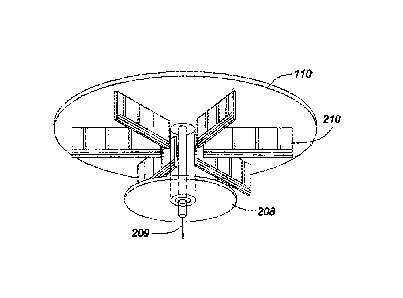
A double-sided PCB monopole Yagi-Uda antenna is disclosed, preferably as part of a directional beam antenna comprising a plurality of such antennas vertically mounted in spoke-like fashion around a metallic antenna PCB substrate. The monopoles are printed on a monopole dielectric substrate. Each antenna comprises a driver, a reflector and a pair of directors, each forming a strip etched at corresponding positions on either side of the PCB and electrically connected at a distal end of the strip by a via passing through the PCB. The driver is connected to the central conductor of a connector, while the reflector and directors are grounded. Because the monopoles are printed on a double-sided PCB, there is no bias in the azimuth pattern of antenna when vertically mounted as contemplated above. The use of a monopole dielectric substrate provides generally more consistent and improved performance over discrete wire monopole Yagi-Uda antennas.


French Abstract

Une antenne Yagi-Uda unipolaire à carte de circuits imprimés double face est décrite, de préférence comme faisant partie dune antenne directionnelle à faisceau comprenant une pluralité de telles antennes fixées verticalement à la manière de rayons dune roue autour dun substrat de carte de circuits imprimés dantenne métallique. Les monopoles sont imprimés sur un substrat diélectrique monopole. Chaque antenne comprend un élément excitateur, un réflecteur et une paire déléments directeurs, chacun formant une bande gravée à des emplacements correspondants de chaque côté de la carte de circuits imprimés et étant connecté électriquement à une extrémité distale de la bande par un trou dinterconnexion traversant la carte. Lantenne est reliée au conducteur central dun connecteur, alors que le réflecteur et les éléments directeurs sont mis à la terre. Comme les monopoles sont imprimés sur une carte de circuits imprimés double face, il ny a aucune polarisation dans le motif dazimut de lantenne lorsquelle est fixée verticalement comme prévu ci-dessus. Lutilisation dun substrat diélectrique unipolaire offre une performance généralement plus homogène et améliorée par rapport aux antennes Yagi-Uda unipolaires à fil distinct.

Claims

Note: Claims are shown in the official language in which they were submitted.


-8-
What is claimed is:
1. A Yagi-Uda monopole antenna printed on each side of a
double-sided printed circuit board wherein each strip element
etched on a first side of the printed circuit board is
electrically connected to a corresponding strip element on a
second side of the printed circuit board by at least one via
hole.
2. The Yagi-Uda monopole antenna according to claim 1,
further comprising a plurality of strip elements identically
etched at corresponding identical positions on each side of the
printed circuit board.
3. The Yagi-Uda monopole antenna according to claim 2,
wherein the distal end of each of the plurality of strip
elements on either side of the printed circuit board are
electrically connected.
4. The Yagi-Uda monopole antenna according to claim 3,
wherein the distal end of each of the plurality of strip
elements on either side of the printed circuit board are
electrically connected by a via hole passing therethrough the
printed circuit board.
5. The Yagi-Uda monopole antenna according to claim 2,
further comprising a reflector.
6. The Yagi-Uda monopole antenna according to claim 5,
wherein the reflector is electrically grounded.

-9-
7. The Yagi-Uda monopole antenna according to claim 2,
further comprising a driver.
8. The Yagi-Uda monopole antenna according to claim 7,
wherein the driver is electrically connected to an internal
conductor of a Sub Miniature Version A (SMA) connector.
9. The Yagi-Uda monopole antenna according to claim 2,
further comprising a plurality of directors.
10. The Yagi-Uda monopole antenna according to claim 9,
wherein at least one of the plurality of directors is
electrically grounded.
11. The Yagi-Uda monopole antenna according to claim 9,
wherein the plurality of directors is two in number, and wherein
the two are both grounded.
12. The Yagi-Uda monopole antenna according to claim 1,
wherein the double-sided printed circuit board is used as an
antenna substrate.
13. A directional beam antenna comprising a plurality of
Yagi-Uda monopole antennas according to claim 1 and a metallic
disk, wherein the plurality of Yagi-Uda monopole antennas are
mounted substantially normal to the metallic disk and radially
outward from an axis thereof in spaced-apart fashion.
14. The directional beam antenna according to claim 13,
wherein the plurality of Yagi-Uda monopole antennas is six in
number.

-10-
15. The directional beam antenna according to claim 13,
wherein the plurality of Yagi-Uda monopole antennas are
substantially equally spaced apart.
16. The directional beam antenna according to claim 13,
wherein the metallic disk is deposited on one side of a PCB
substrate.
17. The directional beam antenna according to claim 13,
wherein the height thereof in a direction normal to the metallic
disk is substantially approximately one quarter of an operating
wavelength of one of the plurality of Yagi-Uda monopole
antennas.

Description

Note: Descriptions are shown in the official language in which they were submitted.


CA 02596025 2007-08-02
1
19207P0021 CA01
A MICROSTRIP DOUBLE SIDED MONOPOLE YAGI-UDA ANTENNA WITH
APPLICATION IN SECTOR ANTENNAS
FIELD OF THE INVENTION
The present invention relates to wireless local area
networks and in particular to a novel Yagi-Uda antenna for
use in such networks.
BACKGROUND TO THE INVENTION
Modern wireless networks rely on suitable antennas
that exhibit desirable performance characteristics while
remaining light weight. In many wireless networks,
multiple independent antennas may be used, whether in
stand-alone mode or as part of a composite antenna.
In most systems, it Is preferable that the performance
of each such antenna be consistent across the board and in
conformance to designed parameters.
With the emergence of new wireless standards for
multiple input multiple output (MIMO) systems, the design
of low profile, high gain, efficient and cheap antennas for
improving the performance of wireless systems has gained
increased importance.
One of the more challenging areas of wireless antenna
design is the implementation of high gain sector antennas
with vertical polarization for wireless local area network
(WLAN) access points.
While a number of different kinds of printed circuit
antennas have been considered for wireless applications,
none of these conventional antennas have proved suitable

CA 2596025 2017-04-28
- 2a -
Attorney Ref: 1227P016CA01
for vertically polarized sector antenna applications. This
includes the so-called Yagi-Uda dipole antenna well known in
the art, for example, as discussed in microstrip form in
United States Patent Nos. 5,712,643 entitled "Planar
Microstrip Yagi Antenna Array" and issued to Skladany on
January 27, 1998, and 7,015,860 entitled "Microstrip Yagi-Uda
Antenna" and issued to Alsliety on March 21, 2006.
The primary difficulty with such conventional antennas is
inserting them in on a common disk in a stable vertical
position and in providing a feed network therefore.
Additionally, the physical height of such antennas would be
half of their operating wavelength.
Accordingly, it is desirable to provide a novel sector
antenna that may be produced in quantities while maintaining
minimum consistent performance characteristics.
Furthermore, it is desirable to provide a novel sector
antenna that maintains stability, good gain, wide bandwidth
and low return loss characteristics.
SUMMARY OF THE INVENTION
In a first aspect, this document discloses a Yagi-Uda
monopole antenna printed on each side of a double-sided
printed circuit board wherein each strip element etched on a
first side of the printed circuit board is electrically
connected to a corresponding strip element on a second side of
the printed circuit board by at least one via hole.
The present invention accomplishes these aims by
providing a double-sided printed-circuit board (PCB) monopole
Yagi-Uda antenna. Preferably, a plurality of such antennas is
vertically mounted in spoke-like fashion around a circular
ground plane deposited on one side of a PCB substrate.

CA 2596025 2017-04-28
- 2b -
Attorney Ref: 1227P016CA01
To assist in manufacturability and reproducibility, the
monopoles are printed on a monopole dielectric substrate,
which provides generally more consistent and

CA 02596025 2007-08-02
- 3 -
19207P0021CA01
improved performance over discrete wire monopole Yagi-Uda
antennas. Because the monopoles are printed on both sides
of the PCB and then connected by vias, there is no bias in
the antenna pattern when vertically mounted as contemplated
above and the resulted pattern would be completely
symmetrical.
According to a broad aspect of an embodiment of the
present invention, there is disclosed a Yagi-Uda monopole
antenna printed on each side of a double-sided printed
circuit board.
According to a second broad aspect of an embodiment of
the present invention, there is disclosed a directional
beam antenna comprising a plurality of such Yagi-Uda
monopole antennas and a metallic disk, wherein the
plurality of Yadi-Uda monopole antennas are mounted
substantially normal to the metallic disk and radially
outward from an axis thereof in spaced-apart fashion.
BRIEF DESCRIPTION OF THE DRAWINGS
The embodiments of the present invention will now be
described by reference to the following figures, in which
identical reference numerals in different figures indicate
identical elements and in which:
Figure 1 is a perspective view of an antenna in
accordance with a preferred embodiment of the present
invention as mounted in an exemplary configuration as part
of a MIMO sub-assembly;

CA 02596025 2007-08-02
- 4 -
19207P0021CA01
Figure 2 is a plan view of the layout of a side of a
double-sided PCB monopole Yagi-Uda antenna used in the MIMO
sub-assembly of Figure 1; and
Figure 3 is a plot of simulated and measured input
reflection for the antenna of Figure 2.
Figure 4 is a plot of measured directivity and gain of
an antenna in accordance with the present invention.
Figure 5 shows a simulated azimuth and elevation
pattern of an antenna in accordance with the present
invention.
DETAILED DESCRIPTION OF THE PREFERRED EMBODIMENTS
Referring now to Figure 1, there is shown a circular
metallic disk 110, preferably deposited upon an antenna PCB
substrate, each of which holds a plurality of directional
beam antennas 210, which each comprise the inventive
double-sided printed circuit monopole Yagi-Uda antenna
vertically oriented around the circumference thereof and
connected by a Sub Miniature Version A (SMA) connector
soldered therewith.
An omni directional antenna 209 is located on a
pedestal 208 at the center of the circular metallic disk
110. This omni directional antenna 209 is a sleeve
monopole on a small circular ground plane 208 and is used
in different operation modes of MIMO application.
Preferably, the circular metallic disk 110 is
deposited on one side of a PCB substrate.

CA 02596025 2007-08-02
- 5 -
19207P0021CA01
Turning now to Figure 2, each of the monopole antennas
210 are printed on both sides of a dielectric substrate
211. The dielectric substrate thickness and permeability
can be a variable in the design.
The use of double-sided PCB manufacturing technology
permits more accurate monopole heights that correspond to
more accurate beam shapes and design flexibility, while
maintaining stability, good gain, wide bandwidth and low
return loss characteristics. Experimental results of
Figures 3, 4 and 5 have shown that performance is also
generally improved over discrete wire monopole Yagi-Uda
antennas with the same number of directors.
Each Yagi-Uda antenna 210 has one reflector 212, one
driver 213 and two director elements 214, 215. It is made
by etching identical strips on both sides of the PCB
dielectric substrate 211. The two identical strips are
connected together with via holes (not clearly shown) that
help to suppress the destructive effect of surface waves.
The double-sided pattern of such an antenna provides both a
symmetrical pattern in the azimuth plane and a higher
radiation efficiency over prior attempts to mass produce
dipole Yagi-Uda antennas using single sided PCB techniques.
Preferably, the monopole dielectric substrate 211 is
thin, of approximately 0.787 mm, to avoid dielectric
losses, and manufactured from the low cost Flame Resistant
4 (FR4) material having a permittivity of 4.2 and a tangent
loss of 0.02.
In a preferred embodiment, each monopole dielectric
substrate has a length of 8 cm and width of 3 cm. To

CA 02596025 2007-08-02
- 6 -
19207P0021CA01
achieve operation in the 2.43 GHz band, as shown in Figure
3, the reflector 212 is preferably 27.5 mm long, the driver
213 is 24.6 mm long, the first director 214 is 21.7 mm long
and the second director 215 is 22.4 mm long. The reflector
212 and driver 213 are separated by 25.5 mm, while the
driver 213 and first 214 and second 215 directors are each
separated by 21.2 mm.
Each strip is preferably 2 mm wide and the distal ends
of each strip are connected through the substrate by vias
218. The central conductor 221 of an SMA connector 219 is
connected to the driver 213 while its ground 222 is
connected to the SMA ground conductors 220 on the antenna
board 211.
The inner conductor 221 of a SMA connector 219 is
preferably soldered to the driver 213 of Yagi-Uda antenna
210, while the reflector 212 and directors 214, 215 are
soldered to ground.
Experimental and simulation results of Figures 3 ,4
and 5 have shown that the double-sided PCB monopole Yagi-
Uda antenna 210 of the present invention exhibits wide
impedance bandwidth and an azimuth beam pattern that is
symmetrical due to the double-sided etching. The
experimental input reflection is well below -10dB through a
bandwidth of 150 MHz without any extra matching circuits.
The monopole implementation has the advantage of being
of shorter length compared to a dipole Yagi-Uda antenna and
an easier feed with good matching. In the preferred
embodiment, the Yagi-Uda monopole antenna 210 has a height
of almost a quarter wavelength, that is, half of the height

CA 02596025 2015-12-01
- 7 -
of conventional printed circuit Yagi-Uda dipole antennas
and thus boasts a low profile.
It will be apparent to those skilled in this art that
various modifications and variations may be made to the
embodiments disclosed herein, consistent with the present
invention, without departing from the spirit and scope of
the present invention.
For example, a Yagr-Uda antenna can be built on
thicker PCBs with higher dielectric constants to reduce the
size. Ground planes with bigger radii can be used to
improve the gain. The number of directors can be increased
to improve the gain. The driver, reflector, or directors,
can be deliberately shaped to improve the matching of the
antenna without adding any extra cost or complexity to the
antenna design. The distance of the Yagi board to the
center of the disk can be used as a parameter to control
the gain and mutual coupling of antennas in a sector
antenna application.
90 Other embodiments consistent with the present
invention will become apparent from consideration of the
specification and the practice of the invention disclosed
therein.

Representative Drawing
A single figure which represents the drawing illustrating the invention.
Administrative Status

2024-08-01:As part of the Next Generation Patents (NGP) transition, the Canadian Patents Database (CPD) now contains a more detailed Event History, which replicates the Event Log of our new back-office solution.

Please note that "Inactive:" events refers to events no longer in use in our new back-office solution.

For a clearer understanding of the status of the application/patent presented on this page, the site Disclaimer , as well as the definitions for Patent , Event History , Maintenance Fee  and Payment History  should be consulted.

Event History

Description Date
Common Representative Appointed 2019-10-30
Appointment of Agent Requirements Determined Compliant 2019-03-18
Inactive: Office letter 2019-03-18
Revocation of Agent Requirements Determined Compliant 2019-03-18
Revocation of Agent Request 2019-02-18
Appointment of Agent Request 2019-02-18
Revocation of Agent Requirements Determined Compliant 2018-11-13
Appointment of Agent Requirements Determined Compliant 2018-11-13
Revocation of Agent Request 2018-10-30
Appointment of Agent Request 2018-10-30
Appointment of Agent Request 2018-06-06
Revocation of Agent Request 2018-06-06
Grant by Issuance 2017-06-27
Inactive: Cover page published 2017-06-26
Amendment After Allowance Requirements Determined Compliant 2017-05-19
Letter Sent 2017-05-19
Amendment After Allowance (AAA) Received 2017-04-28
Pre-grant 2017-04-28
Inactive: Amendment after Allowance Fee Processed 2017-04-28
Inactive: Final fee received 2017-04-28
Notice of Allowance is Issued 2016-11-25
Letter Sent 2016-11-25
Notice of Allowance is Issued 2016-11-25
Inactive: Q2 passed 2016-11-22
Inactive: Approved for allowance (AFA) 2016-11-22
Amendment Received - Voluntary Amendment 2016-09-29
Inactive: S.30(2) Rules - Examiner requisition 2016-04-13
Inactive: Report - No QC 2016-04-13
Inactive: Office letter 2016-04-08
Revocation of Agent Requirements Determined Compliant 2016-04-08
Appointment of Agent Requirements Determined Compliant 2016-04-08
Appointment of Agent Request 2016-03-18
Revocation of Agent Request 2016-03-18
Letter Sent 2016-02-12
Letter Sent 2015-12-04
Amendment Received - Voluntary Amendment 2015-12-01
Reinstatement Requirements Deemed Compliant for All Abandonment Reasons 2015-12-01
Reinstatement Request Received 2015-12-01
Inactive: Abandoned - No reply to s.30(2) Rules requisition 2014-12-04
Inactive: S.30(2) Rules - Examiner requisition 2014-06-04
Inactive: Report - No QC 2014-05-23
Letter Sent 2012-08-20
All Requirements for Examination Determined Compliant 2012-08-02
Request for Examination Requirements Determined Compliant 2012-08-02
Request for Examination Received 2012-08-02
Letter Sent 2012-02-03
Inactive: Office letter 2012-02-03
Letter Sent 2010-05-27
Inactive: Cover page published 2008-04-20
Application Published (Open to Public Inspection) 2008-04-20
Inactive: IPC assigned 2008-01-03
Inactive: First IPC assigned 2008-01-03
Inactive: IPC assigned 2008-01-03
Inactive: Filing certificate - No RFE (English) 2007-08-31
Application Received - Regular National 2007-08-31

Abandonment History

Abandonment Date Reason Reinstatement Date
2015-12-01

Maintenance Fee

The last payment was received on 2016-04-13

Note : If the full payment has not been received on or before the date indicated, a further fee may be required which may be one of the following

  • the reinstatement fee;
  • the late payment fee; or
  • additional fee to reverse deemed expiry.

Patent fees are adjusted on the 1st of January every year. The amounts above are the current amounts if received by December 31 of the current year.
Please refer to the CIPO Patent Fees web page to see all current fee amounts.

Owners on Record

Note: Records showing the ownership history in alphabetical order.

Current Owners on Record
COMMUNICATION COMPONENTS ANTENNA INC.
Past Owners on Record
JOHN LITVA
NASRIN HOJJAT
Past Owners that do not appear in the "Owners on Record" listing will appear in other documentation within the application.
Documents

To view selected files, please enter reCAPTCHA code :


To view images, click a link in the Document Description column (Temporarily unavailable). To download the documents, select one or more checkboxes in the first column and then click the "Download Selected in PDF format (Zip Archive)" or the "Download Selected as Single PDF" button.

List of published and non-published patent-specific documents on the CPD .

If you have any difficulty accessing content, you can call the Client Service Centre at 1-866-997-1936 or send them an e-mail at CIPO Client Service Centre.

({010=All Documents, 020=As Filed, 030=As Open to Public Inspection, 040=At Issuance, 050=Examination, 060=Incoming Correspondence, 070=Miscellaneous, 080=Outgoing Correspondence, 090=Payment})


Document
Description 
Date
(yyyy-mm-dd) 
Number of pages   Size of Image (KB) 
Representative drawing 2017-05-29 1 15
Description 2007-08-01 7 249
Abstract 2007-08-01 1 25
Claims 2007-08-01 3 72
Drawings 2007-08-01 5 73
Representative drawing 2008-03-24 1 22
Description 2015-11-30 7 244
Claims 2015-11-30 3 67
Claims 2016-09-28 3 68
Description 2017-04-27 8 232
Maintenance fee payment 2024-05-14 2 69
Filing Certificate (English) 2007-08-30 1 158
Reminder of maintenance fee due 2009-04-05 1 112
Reminder - Request for Examination 2012-04-02 1 118
Acknowledgement of Request for Examination 2012-08-19 1 175
Courtesy - Abandonment Letter (R30(2)) 2015-01-28 1 164
Notice of Reinstatement 2015-12-03 1 170
Commissioner's Notice - Application Found Allowable 2016-11-24 1 161
Correspondence 2012-02-02 1 14
Fees 2015-07-30 1 25
Amendment / response to report 2015-11-30 14 337
Correspondence 2016-03-17 3 116
Courtesy - Office Letter 2016-04-07 1 21
Courtesy - Office Letter 2016-04-07 2 44
Examiner Requisition 2016-04-12 3 210
Amendment / response to report 2016-09-28 7 187
Amendment after allowance / Amendment / response to report 2017-04-27 5 134
Final fee 2017-04-27 3 90
Courtesy - Acknowledgment of Acceptance of Amendment after Notice of Allowance 2017-05-18 1 40
Change of agent 2019-02-17 4 141
Courtesy - Office Letter 2019-03-17 1 26