Sélection de la langue

Search

Sommaire du brevet 2596025 

Énoncé de désistement de responsabilité concernant l'information provenant de tiers

Une partie des informations de ce site Web a été fournie par des sources externes. Le gouvernement du Canada n'assume aucune responsabilité concernant la précision, l'actualité ou la fiabilité des informations fournies par les sources externes. Les utilisateurs qui désirent employer cette information devraient consulter directement la source des informations. Le contenu fourni par les sources externes n'est pas assujetti aux exigences sur les langues officielles, la protection des renseignements personnels et l'accessibilité.

Disponibilité de l'Abrégé et des Revendications

L'apparition de différences dans le texte et l'image des Revendications et de l'Abrégé dépend du moment auquel le document est publié. Les textes des Revendications et de l'Abrégé sont affichés :

  • lorsque la demande peut être examinée par le public;
  • lorsque le brevet est émis (délivrance).
(12) Brevet: (11) CA 2596025
(54) Titre français: UNE ANTENNE YAGI-UDA UNIPOLAIRE A LIGNE MICRORUBAN DOUBLE FACE AVEC APPLICATION COMME ANTENNES SECTORIELLES
(54) Titre anglais: A MICROSTRIP DOUBLE SIDED MONOPOLE YAGI-UDA ANTENNA WITH APPLICATION IN SECTOR ANTENNAS
Statut: Accordé et délivré
Données bibliographiques
(51) Classification internationale des brevets (CIB):
  • H01Q 19/30 (2006.01)
  • H01Q 01/38 (2006.01)
(72) Inventeurs :
  • LITVA, JOHN (Canada)
  • HOJJAT, NASRIN (Canada)
(73) Titulaires :
  • COMMUNICATION COMPONENTS ANTENNA INC.
(71) Demandeurs :
  • COMMUNICATION COMPONENTS ANTENNA INC. (Canada)
(74) Agent: ROBIC AGENCE PI S.E.C./ROBIC IP AGENCY LP
(74) Co-agent:
(45) Délivré: 2017-06-27
(22) Date de dépôt: 2007-08-02
(41) Mise à la disponibilité du public: 2008-04-20
Requête d'examen: 2012-08-02
Licence disponible: S.O.
Cédé au domaine public: S.O.
(25) Langue des documents déposés: Anglais

Traité de coopération en matière de brevets (PCT): Non

(30) Données de priorité de la demande:
Numéro de la demande Pays / territoire Date
2,565,032 (Canada) 2006-10-20

Abrégés

Abrégé français

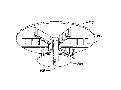
Une antenne Yagi-Uda unipolaire à carte de circuits imprimés double face est décrite, de préférence comme faisant partie dune antenne directionnelle à faisceau comprenant une pluralité de telles antennes fixées verticalement à la manière de rayons dune roue autour dun substrat de carte de circuits imprimés dantenne métallique. Les monopoles sont imprimés sur un substrat diélectrique monopole. Chaque antenne comprend un élément excitateur, un réflecteur et une paire déléments directeurs, chacun formant une bande gravée à des emplacements correspondants de chaque côté de la carte de circuits imprimés et étant connecté électriquement à une extrémité distale de la bande par un trou dinterconnexion traversant la carte. Lantenne est reliée au conducteur central dun connecteur, alors que le réflecteur et les éléments directeurs sont mis à la terre. Comme les monopoles sont imprimés sur une carte de circuits imprimés double face, il ny a aucune polarisation dans le motif dazimut de lantenne lorsquelle est fixée verticalement comme prévu ci-dessus. Lutilisation dun substrat diélectrique unipolaire offre une performance généralement plus homogène et améliorée par rapport aux antennes Yagi-Uda unipolaires à fil distinct.


Abrégé anglais

A double-sided PCB monopole Yagi-Uda antenna is disclosed, preferably as part of a directional beam antenna comprising a plurality of such antennas vertically mounted in spoke-like fashion around a metallic antenna PCB substrate. The monopoles are printed on a monopole dielectric substrate. Each antenna comprises a driver, a reflector and a pair of directors, each forming a strip etched at corresponding positions on either side of the PCB and electrically connected at a distal end of the strip by a via passing through the PCB. The driver is connected to the central conductor of a connector, while the reflector and directors are grounded. Because the monopoles are printed on a double-sided PCB, there is no bias in the azimuth pattern of antenna when vertically mounted as contemplated above. The use of a monopole dielectric substrate provides generally more consistent and improved performance over discrete wire monopole Yagi-Uda antennas.

Revendications

Note : Les revendications sont présentées dans la langue officielle dans laquelle elles ont été soumises.


-8-
What is claimed is:
1. A Yagi-Uda monopole antenna printed on each side of a
double-sided printed circuit board wherein each strip element
etched on a first side of the printed circuit board is
electrically connected to a corresponding strip element on a
second side of the printed circuit board by at least one via
hole.
2. The Yagi-Uda monopole antenna according to claim 1,
further comprising a plurality of strip elements identically
etched at corresponding identical positions on each side of the
printed circuit board.
3. The Yagi-Uda monopole antenna according to claim 2,
wherein the distal end of each of the plurality of strip
elements on either side of the printed circuit board are
electrically connected.
4. The Yagi-Uda monopole antenna according to claim 3,
wherein the distal end of each of the plurality of strip
elements on either side of the printed circuit board are
electrically connected by a via hole passing therethrough the
printed circuit board.
5. The Yagi-Uda monopole antenna according to claim 2,
further comprising a reflector.
6. The Yagi-Uda monopole antenna according to claim 5,
wherein the reflector is electrically grounded.

-9-
7. The Yagi-Uda monopole antenna according to claim 2,
further comprising a driver.
8. The Yagi-Uda monopole antenna according to claim 7,
wherein the driver is electrically connected to an internal
conductor of a Sub Miniature Version A (SMA) connector.
9. The Yagi-Uda monopole antenna according to claim 2,
further comprising a plurality of directors.
10. The Yagi-Uda monopole antenna according to claim 9,
wherein at least one of the plurality of directors is
electrically grounded.
11. The Yagi-Uda monopole antenna according to claim 9,
wherein the plurality of directors is two in number, and wherein
the two are both grounded.
12. The Yagi-Uda monopole antenna according to claim 1,
wherein the double-sided printed circuit board is used as an
antenna substrate.
13. A directional beam antenna comprising a plurality of
Yagi-Uda monopole antennas according to claim 1 and a metallic
disk, wherein the plurality of Yagi-Uda monopole antennas are
mounted substantially normal to the metallic disk and radially
outward from an axis thereof in spaced-apart fashion.
14. The directional beam antenna according to claim 13,
wherein the plurality of Yagi-Uda monopole antennas is six in
number.

-10-
15. The directional beam antenna according to claim 13,
wherein the plurality of Yagi-Uda monopole antennas are
substantially equally spaced apart.
16. The directional beam antenna according to claim 13,
wherein the metallic disk is deposited on one side of a PCB
substrate.
17. The directional beam antenna according to claim 13,
wherein the height thereof in a direction normal to the metallic
disk is substantially approximately one quarter of an operating
wavelength of one of the plurality of Yagi-Uda monopole
antennas.

Description

Note : Les descriptions sont présentées dans la langue officielle dans laquelle elles ont été soumises.


CA 02596025 2007-08-02
1
19207P0021 CA01
A MICROSTRIP DOUBLE SIDED MONOPOLE YAGI-UDA ANTENNA WITH
APPLICATION IN SECTOR ANTENNAS
FIELD OF THE INVENTION
The present invention relates to wireless local area
networks and in particular to a novel Yagi-Uda antenna for
use in such networks.
BACKGROUND TO THE INVENTION
Modern wireless networks rely on suitable antennas
that exhibit desirable performance characteristics while
remaining light weight. In many wireless networks,
multiple independent antennas may be used, whether in
stand-alone mode or as part of a composite antenna.
In most systems, it Is preferable that the performance
of each such antenna be consistent across the board and in
conformance to designed parameters.
With the emergence of new wireless standards for
multiple input multiple output (MIMO) systems, the design
of low profile, high gain, efficient and cheap antennas for
improving the performance of wireless systems has gained
increased importance.
One of the more challenging areas of wireless antenna
design is the implementation of high gain sector antennas
with vertical polarization for wireless local area network
(WLAN) access points.
While a number of different kinds of printed circuit
antennas have been considered for wireless applications,
none of these conventional antennas have proved suitable

CA 2596025 2017-04-28
- 2a -
Attorney Ref: 1227P016CA01
for vertically polarized sector antenna applications. This
includes the so-called Yagi-Uda dipole antenna well known in
the art, for example, as discussed in microstrip form in
United States Patent Nos. 5,712,643 entitled "Planar
Microstrip Yagi Antenna Array" and issued to Skladany on
January 27, 1998, and 7,015,860 entitled "Microstrip Yagi-Uda
Antenna" and issued to Alsliety on March 21, 2006.
The primary difficulty with such conventional antennas is
inserting them in on a common disk in a stable vertical
position and in providing a feed network therefore.
Additionally, the physical height of such antennas would be
half of their operating wavelength.
Accordingly, it is desirable to provide a novel sector
antenna that may be produced in quantities while maintaining
minimum consistent performance characteristics.
Furthermore, it is desirable to provide a novel sector
antenna that maintains stability, good gain, wide bandwidth
and low return loss characteristics.
SUMMARY OF THE INVENTION
In a first aspect, this document discloses a Yagi-Uda
monopole antenna printed on each side of a double-sided
printed circuit board wherein each strip element etched on a
first side of the printed circuit board is electrically
connected to a corresponding strip element on a second side of
the printed circuit board by at least one via hole.
The present invention accomplishes these aims by
providing a double-sided printed-circuit board (PCB) monopole
Yagi-Uda antenna. Preferably, a plurality of such antennas is
vertically mounted in spoke-like fashion around a circular
ground plane deposited on one side of a PCB substrate.

CA 2596025 2017-04-28
- 2b -
Attorney Ref: 1227P016CA01
To assist in manufacturability and reproducibility, the
monopoles are printed on a monopole dielectric substrate,
which provides generally more consistent and

CA 02596025 2007-08-02
- 3 -
19207P0021CA01
improved performance over discrete wire monopole Yagi-Uda
antennas. Because the monopoles are printed on both sides
of the PCB and then connected by vias, there is no bias in
the antenna pattern when vertically mounted as contemplated
above and the resulted pattern would be completely
symmetrical.
According to a broad aspect of an embodiment of the
present invention, there is disclosed a Yagi-Uda monopole
antenna printed on each side of a double-sided printed
circuit board.
According to a second broad aspect of an embodiment of
the present invention, there is disclosed a directional
beam antenna comprising a plurality of such Yagi-Uda
monopole antennas and a metallic disk, wherein the
plurality of Yadi-Uda monopole antennas are mounted
substantially normal to the metallic disk and radially
outward from an axis thereof in spaced-apart fashion.
BRIEF DESCRIPTION OF THE DRAWINGS
The embodiments of the present invention will now be
described by reference to the following figures, in which
identical reference numerals in different figures indicate
identical elements and in which:
Figure 1 is a perspective view of an antenna in
accordance with a preferred embodiment of the present
invention as mounted in an exemplary configuration as part
of a MIMO sub-assembly;

CA 02596025 2007-08-02
- 4 -
19207P0021CA01
Figure 2 is a plan view of the layout of a side of a
double-sided PCB monopole Yagi-Uda antenna used in the MIMO
sub-assembly of Figure 1; and
Figure 3 is a plot of simulated and measured input
reflection for the antenna of Figure 2.
Figure 4 is a plot of measured directivity and gain of
an antenna in accordance with the present invention.
Figure 5 shows a simulated azimuth and elevation
pattern of an antenna in accordance with the present
invention.
DETAILED DESCRIPTION OF THE PREFERRED EMBODIMENTS
Referring now to Figure 1, there is shown a circular
metallic disk 110, preferably deposited upon an antenna PCB
substrate, each of which holds a plurality of directional
beam antennas 210, which each comprise the inventive
double-sided printed circuit monopole Yagi-Uda antenna
vertically oriented around the circumference thereof and
connected by a Sub Miniature Version A (SMA) connector
soldered therewith.
An omni directional antenna 209 is located on a
pedestal 208 at the center of the circular metallic disk
110. This omni directional antenna 209 is a sleeve
monopole on a small circular ground plane 208 and is used
in different operation modes of MIMO application.
Preferably, the circular metallic disk 110 is
deposited on one side of a PCB substrate.

CA 02596025 2007-08-02
- 5 -
19207P0021CA01
Turning now to Figure 2, each of the monopole antennas
210 are printed on both sides of a dielectric substrate
211. The dielectric substrate thickness and permeability
can be a variable in the design.
The use of double-sided PCB manufacturing technology
permits more accurate monopole heights that correspond to
more accurate beam shapes and design flexibility, while
maintaining stability, good gain, wide bandwidth and low
return loss characteristics. Experimental results of
Figures 3, 4 and 5 have shown that performance is also
generally improved over discrete wire monopole Yagi-Uda
antennas with the same number of directors.
Each Yagi-Uda antenna 210 has one reflector 212, one
driver 213 and two director elements 214, 215. It is made
by etching identical strips on both sides of the PCB
dielectric substrate 211. The two identical strips are
connected together with via holes (not clearly shown) that
help to suppress the destructive effect of surface waves.
The double-sided pattern of such an antenna provides both a
symmetrical pattern in the azimuth plane and a higher
radiation efficiency over prior attempts to mass produce
dipole Yagi-Uda antennas using single sided PCB techniques.
Preferably, the monopole dielectric substrate 211 is
thin, of approximately 0.787 mm, to avoid dielectric
losses, and manufactured from the low cost Flame Resistant
4 (FR4) material having a permittivity of 4.2 and a tangent
loss of 0.02.
In a preferred embodiment, each monopole dielectric
substrate has a length of 8 cm and width of 3 cm. To

CA 02596025 2007-08-02
- 6 -
19207P0021CA01
achieve operation in the 2.43 GHz band, as shown in Figure
3, the reflector 212 is preferably 27.5 mm long, the driver
213 is 24.6 mm long, the first director 214 is 21.7 mm long
and the second director 215 is 22.4 mm long. The reflector
212 and driver 213 are separated by 25.5 mm, while the
driver 213 and first 214 and second 215 directors are each
separated by 21.2 mm.
Each strip is preferably 2 mm wide and the distal ends
of each strip are connected through the substrate by vias
218. The central conductor 221 of an SMA connector 219 is
connected to the driver 213 while its ground 222 is
connected to the SMA ground conductors 220 on the antenna
board 211.
The inner conductor 221 of a SMA connector 219 is
preferably soldered to the driver 213 of Yagi-Uda antenna
210, while the reflector 212 and directors 214, 215 are
soldered to ground.
Experimental and simulation results of Figures 3 ,4
and 5 have shown that the double-sided PCB monopole Yagi-
Uda antenna 210 of the present invention exhibits wide
impedance bandwidth and an azimuth beam pattern that is
symmetrical due to the double-sided etching. The
experimental input reflection is well below -10dB through a
bandwidth of 150 MHz without any extra matching circuits.
The monopole implementation has the advantage of being
of shorter length compared to a dipole Yagi-Uda antenna and
an easier feed with good matching. In the preferred
embodiment, the Yagi-Uda monopole antenna 210 has a height
of almost a quarter wavelength, that is, half of the height

CA 02596025 2015-12-01
- 7 -
of conventional printed circuit Yagi-Uda dipole antennas
and thus boasts a low profile.
It will be apparent to those skilled in this art that
various modifications and variations may be made to the
embodiments disclosed herein, consistent with the present
invention, without departing from the spirit and scope of
the present invention.
For example, a Yagr-Uda antenna can be built on
thicker PCBs with higher dielectric constants to reduce the
size. Ground planes with bigger radii can be used to
improve the gain. The number of directors can be increased
to improve the gain. The driver, reflector, or directors,
can be deliberately shaped to improve the matching of the
antenna without adding any extra cost or complexity to the
antenna design. The distance of the Yagi board to the
center of the disk can be used as a parameter to control
the gain and mutual coupling of antennas in a sector
antenna application.
90 Other embodiments consistent with the present
invention will become apparent from consideration of the
specification and the practice of the invention disclosed
therein.

Dessin représentatif
Une figure unique qui représente un dessin illustrant l'invention.
États administratifs

2024-08-01 : Dans le cadre de la transition vers les Brevets de nouvelle génération (BNG), la base de données sur les brevets canadiens (BDBC) contient désormais un Historique d'événement plus détaillé, qui reproduit le Journal des événements de notre nouvelle solution interne.

Veuillez noter que les événements débutant par « Inactive : » se réfèrent à des événements qui ne sont plus utilisés dans notre nouvelle solution interne.

Pour une meilleure compréhension de l'état de la demande ou brevet qui figure sur cette page, la rubrique Mise en garde , et les descriptions de Brevet , Historique d'événement , Taxes périodiques et Historique des paiements devraient être consultées.

Historique d'événement

Description Date
Représentant commun nommé 2019-10-30
Exigences relatives à la nomination d'un agent - jugée conforme 2019-03-18
Inactive : Lettre officielle 2019-03-18
Exigences relatives à la révocation de la nomination d'un agent - jugée conforme 2019-03-18
Demande visant la révocation de la nomination d'un agent 2019-02-18
Demande visant la nomination d'un agent 2019-02-18
Exigences relatives à la révocation de la nomination d'un agent - jugée conforme 2018-11-13
Exigences relatives à la nomination d'un agent - jugée conforme 2018-11-13
Demande visant la révocation de la nomination d'un agent 2018-10-30
Demande visant la nomination d'un agent 2018-10-30
Demande visant la nomination d'un agent 2018-06-06
Demande visant la révocation de la nomination d'un agent 2018-06-06
Accordé par délivrance 2017-06-27
Inactive : Page couverture publiée 2017-06-26
Exigences de modification après acceptation - jugée conforme 2017-05-19
Lettre envoyée 2017-05-19
Modification après acceptation reçue 2017-04-28
Préoctroi 2017-04-28
Inactive : Taxe de modif. après accept. traitée 2017-04-28
Inactive : Taxe finale reçue 2017-04-28
Un avis d'acceptation est envoyé 2016-11-25
Lettre envoyée 2016-11-25
Un avis d'acceptation est envoyé 2016-11-25
Inactive : Q2 réussi 2016-11-22
Inactive : Approuvée aux fins d'acceptation (AFA) 2016-11-22
Modification reçue - modification volontaire 2016-09-29
Inactive : Dem. de l'examinateur par.30(2) Règles 2016-04-13
Inactive : Rapport - Aucun CQ 2016-04-13
Inactive : Lettre officielle 2016-04-08
Exigences relatives à la révocation de la nomination d'un agent - jugée conforme 2016-04-08
Exigences relatives à la nomination d'un agent - jugée conforme 2016-04-08
Demande visant la nomination d'un agent 2016-03-18
Demande visant la révocation de la nomination d'un agent 2016-03-18
Lettre envoyée 2016-02-12
Lettre envoyée 2015-12-04
Modification reçue - modification volontaire 2015-12-01
Exigences de rétablissement - réputé conforme pour tous les motifs d'abandon 2015-12-01
Requête en rétablissement reçue 2015-12-01
Inactive : Abandon. - Aucune rép dem par.30(2) Règles 2014-12-04
Inactive : Dem. de l'examinateur par.30(2) Règles 2014-06-04
Inactive : Rapport - Aucun CQ 2014-05-23
Lettre envoyée 2012-08-20
Toutes les exigences pour l'examen - jugée conforme 2012-08-02
Exigences pour une requête d'examen - jugée conforme 2012-08-02
Requête d'examen reçue 2012-08-02
Lettre envoyée 2012-02-03
Inactive : Lettre officielle 2012-02-03
Lettre envoyée 2010-05-27
Inactive : Page couverture publiée 2008-04-20
Demande publiée (accessible au public) 2008-04-20
Inactive : CIB attribuée 2008-01-03
Inactive : CIB en 1re position 2008-01-03
Inactive : CIB attribuée 2008-01-03
Inactive : Certificat de dépôt - Sans RE (Anglais) 2007-08-31
Demande reçue - nationale ordinaire 2007-08-31

Historique d'abandonnement

Date d'abandonnement Raison Date de rétablissement
2015-12-01

Taxes périodiques

Le dernier paiement a été reçu le 2016-04-13

Avis : Si le paiement en totalité n'a pas été reçu au plus tard à la date indiquée, une taxe supplémentaire peut être imposée, soit une des taxes suivantes :

  • taxe de rétablissement ;
  • taxe pour paiement en souffrance ; ou
  • taxe additionnelle pour le renversement d'une péremption réputée.

Les taxes sur les brevets sont ajustées au 1er janvier de chaque année. Les montants ci-dessus sont les montants actuels s'ils sont reçus au plus tard le 31 décembre de l'année en cours.
Veuillez vous référer à la page web des taxes sur les brevets de l'OPIC pour voir tous les montants actuels des taxes.

Titulaires au dossier

Les titulaires actuels et antérieures au dossier sont affichés en ordre alphabétique.

Titulaires actuels au dossier
COMMUNICATION COMPONENTS ANTENNA INC.
Titulaires antérieures au dossier
JOHN LITVA
NASRIN HOJJAT
Les propriétaires antérieurs qui ne figurent pas dans la liste des « Propriétaires au dossier » apparaîtront dans d'autres documents au dossier.
Documents

Pour visionner les fichiers sélectionnés, entrer le code reCAPTCHA :


Pour visualiser une image, cliquer sur un lien dans la colonne description du document (Temporairement non-disponible). Pour télécharger l'image (les images), cliquer l'une ou plusieurs cases à cocher dans la première colonne et ensuite cliquer sur le bouton "Télécharger sélection en format PDF (archive Zip)" ou le bouton "Télécharger sélection (en un fichier PDF fusionné)".

Liste des documents de brevet publiés et non publiés sur la BDBC .

Si vous avez des difficultés à accéder au contenu, veuillez communiquer avec le Centre de services à la clientèle au 1-866-997-1936, ou envoyer un courriel au Centre de service à la clientèle de l'OPIC.

({010=Tous les documents, 020=Au moment du dépôt, 030=Au moment de la mise à la disponibilité du public, 040=À la délivrance, 050=Examen, 060=Correspondance reçue, 070=Divers, 080=Correspondance envoyée, 090=Paiement})


Description du
Document 
Date
(aaaa-mm-jj) 
Nombre de pages   Taille de l'image (Ko) 
Dessin représentatif 2017-05-29 1 15
Description 2007-08-01 7 249
Abrégé 2007-08-01 1 25
Revendications 2007-08-01 3 72
Dessins 2007-08-01 5 73
Dessin représentatif 2008-03-24 1 22
Description 2015-11-30 7 244
Revendications 2015-11-30 3 67
Revendications 2016-09-28 3 68
Description 2017-04-27 8 232
Paiement de taxe périodique 2024-05-14 2 69
Certificat de dépôt (anglais) 2007-08-30 1 158
Rappel de taxe de maintien due 2009-04-05 1 112
Rappel - requête d'examen 2012-04-02 1 118
Accusé de réception de la requête d'examen 2012-08-19 1 175
Courtoisie - Lettre d'abandon (R30(2)) 2015-01-28 1 164
Avis de retablissement 2015-12-03 1 170
Avis du commissaire - Demande jugée acceptable 2016-11-24 1 161
Correspondance 2012-02-02 1 14
Taxes 2015-07-30 1 25
Modification / réponse à un rapport 2015-11-30 14 337
Correspondance 2016-03-17 3 116
Courtoisie - Lettre du bureau 2016-04-07 1 21
Courtoisie - Lettre du bureau 2016-04-07 2 44
Demande de l'examinateur 2016-04-12 3 210
Modification / réponse à un rapport 2016-09-28 7 187
Modification après acceptation / Modification / réponse à un rapport 2017-04-27 5 134
Taxe finale 2017-04-27 3 90
Courtoisie - Accusé d’acceptation de modification après l’avis d’acceptation 2017-05-18 1 40
Changement de nomination d'agent 2019-02-17 4 141
Courtoisie - Lettre du bureau 2019-03-17 1 26