Note: Descriptions are shown in the official language in which they were submitted.
CA 02596258 2007-07-27
WO 2006/081668 PCT/CA2006/000143
METHOD AND APPARATUS FOR INITIALIZING A DELAY LOCKED LOOP
BACKGROUND OF THE INVENTION
Fig. 1 is a block diagram of a prior art conventional Delay Locked Loop (DLL)
100.
The main function of a DLL is to synchronize two clock signals by aligning
their rising
edges. An externally supplied clock signal CK is buffered by clock buffer 101
to provide
a reference clock signal CKref that is coupled to a voltage controlled delay
line (VCDL)
102 and a phase detector (PD) 104. The voltage controlled delay line 102
produces a DLL
output clock signal CKout, which is a delayed version of CKref and is routed
to various
circuits within a device through a buffering structure referred to as a clock
tree.
A feedback clock signal CKf is tapped at a terminal node of a branch of the
clock
tree or obtained by applying the output clock signal CKout to a replica of the
clock tree
branch, that is, a replica delay circuit 103 and fed back to the PD 104. The
replica delay
circuit 103 also known as a delay model or a clock tree branch replica,
reproduces all
delays added to the output clock signal CKout by the multi-stage buffering
structure of the
clock tree. The delays include all propagation delays through the logical
gates and buffers
and delays caused by parasitic impedance of long wires. The final synchronised
version of
the feedback clock signal CKf is output at the end of every branch of the
clock tree. The
delay produced by the VCDL 102 is variable and controllable through a variable
control
voltage Vc applied to the VCDL 102. The ability to vary the delay produced by
the
VCDL 102 is used by the DLL 100 to synchronize the reference clock signal
CKref and
the feedback clock signal CKf by aligning the rising edges of the clock
signals (CKref,
CKf).
The phase detector 104 typically generates variable width pulses on the UP and
DOWN output signals dependent on the phase difference between the reference
clock
signal CKref and the feedback clock signal CKf. The variable width pulses on
the UP and
DOWN output signals are integrated by a charge pump 105 and a loop filter 106
coupled
to the output of the charge pump 105 in order to provide the variable control
voltage Vc
for the VCDL 102. The control voltage Vc determines the delay to be added to
the
reference clock signal CKref by the VCDL 102 to align the rising edges of the
feedback
clock signal CKf and reference clock signal CKref. Together, charge pump 105
and loop
filter 106 constitute a control voltage generator 107.
CA 02596258 2007-07-27
WO 2006/081668 PCT/CA2006/000143
Fig 2 is a graph illustrating a typical control voltage Vc vs. controlled
delay
characteristic. The characteristic is non-linear and includes a flat region
202, an optimum
region 200 and a steep region 204. In the flat region 202, a wide variation in
the control
voltage Vc is required for a relatively small delay range.
In the steep region 204, a small variation in the control voltage Vc provides
a large
delay range. Thus, the VCDL has a very high sensitivity in the steep region
204 because a
small noise disturbance on the control voltage Vc results in a large variation
in delay
resulting in an increase in clock jitter. It is also more difficult to provide
stable, non-
oscillating loop operation with such a high sensitivity.
In the "optimum region" 200, the change in delay with respect to change in
control
voltage is moderate. Thus, the DLL 100 operates in the "optimum region"
without
oscillating, drifting or accumulating noise.
A lock point is any point in the characteristic to which a DLL can lock. There
can
be a plurality of lock points on the characteristic. The operating point is
the lock point to
which the DLL is locked during normal operation. One important aspect in
designing a
DLL is choosing the correct operating point in the characteristic and steering
the DLL to
reach and lock to that operating point quickly after power-up or reset. This
process is
typically referred to as DLL initialization. Proper initialization of the DLL
ensures good
DLL performance and a steady lock.
Selecting the correct operating point sets the control voltage Vc to a target
voltage
level related to a stable operation region. To ensure stable DLL operation,
the DLL should
be initialized to an operating point in the "optimum region" 200 of the VCDL
delay vs.
control voltage characteristic.
After the DLL has reached the operating point, the operating point can move
due to
changes in operating conditions such as temperature and power supply. Thus,
another
important aspect of DLL design is to keep the operating point within
predetermined limits
of the lock point on the delay vs. voltage characteristic while operating
conditions change.
The variation in the control voltage Vc is limited to the variation in power
supply voltage
at most, often the variation in the control voltage Vc is smaller than the
variation in the
power supply voltage. Therefore, the delay vs. control voltage characteristic
shown in Fig.
2 is not infinite on both ends and it is possible that as operating conditions
change, the
operating point can drift to either the left or right limit of the
characteristic and the DLL
will eventually lose lock. This has a particularly high probability of
occurring if the DLL
2
CA 02596258 2007-07-27
WO 2006/081668 PCT/CA2006/000143
is initialised to an operating point that is too close to either of the two
ends of the
characteristic.
It is preferable to lock the operating point to a lock point on the left side
of the
characteristic because this is the region with better noise immunity. However,
if the
operating point is too close to the left end of the characteristic, it is
possible for the DLL to
reach the left limit of the characteristic due to changes in operating
conditions. This
situation is illustrated in Figs. 3A and 3B.
Fig. 3A is a graph illustrating a lock point 300 that is close to the left end
of the
control voltage v. delay characteristic. Fig. 3B is a clock signal timing
diagram
corresponding to the control voltage v. delay characteristic in Fig. 3A. The
operating
point is at lock point 300 in nominal conditions. A range of delay 302 in the
VCDL is
required to compensate for variations in operating conditions. Referring to
the clock
signal timing diagram, the drift in the rising edge of the feedback clock
signal CKf 304
corresponds to the range of delay 302 shown in the graph in Fig. 3A. The
minimum delay
306 in the delay range 302 is beyond the full range of delays produced by the
VCDL 310
as illustrated by the gap in the delay range 308. Thus, the operating point
can move to the
end of the VCDL range causing the DLL to lose lock.
Another potential risk is for the DLL to start searching for a lock point from
a
random point on the characteristic during start-up with no restriction on the
search
direction. As the externally supplied clock signal CK is free running, the
initial phase
relationship between the feedback clock signal CKf and the reference clock
signal CKref
after a reset or power-up is not known. Also, after power-up or reset, the
position of the
initial DLL unlocked operating point is unknown and can be anywhere on the
characteristic. Thus, the VCDL delay can be initially increased or decreased
dependent on
whether the rising edge of the feedback clock signal CKf or the rising edge of
the
reference clock signal CKref is detected first by the PD 104 (Fig. 1).
Therefore, the
direction in which the VCDL delay is initially adjusted is unpredictable.
Fig. 4A is a graph illustrating an initial search for a lock point in a search
direction
that results in hitting the delay limit of the VCDL 102 (Fig. 1) before lock
can be reached.
Fig. 4B is a clock signal timing diagram corresponding to the search shown in
Fig. 4A.
The search for the lock point begins at random search point 400. If the DLL
starts from a
point close to an end of the characteristic and proceeds towards that end, it
can hit the
delay limit of the VCDL before lock can be reached. In the example shown in
Figs. 4A-
3
CA 02596258 2007-07-27
WO 2006/081668 PCT/CA2006/000143
4B, during initialization, the DLL unpredictably moves toward the nearest lock
point 402
which is beyond the VCDL range and cannot be reached. For example, this
situation can
occur if the phase detector 104 (Fig. 1) initially produces UP/DOWN pulses
that steer the
DLL 100 in the direction of the closest lock point 402 that is beyond the VCDL
range 310.
The range of the variable VCDL delay in a DLL is also important. Normally, the
range of variable VCDL delay is calculated so that the smallest delay
corresponds to a
clock frequency somewhat higher than that which the DLL specification requires
and the
largest delay corresponds to a somewhat lower clock frequency. The variable
VCDL
delay is calculated in order to ensure margins. For a DLL that is designed to
operate over
a wide clock frequency range, that is, when the clock period is not a constant
value and all
the possible values are to be accommodated by the same VCDL, the VCDL has to
produce
an even wider range of delays. As a result, typically there are a number of
possible lock
points on the VCDL characteristic for a clock signal having a particular
frequency. For
higher clock frequencies, the VCDL can produce a delay that is longer than a
multiple of
the clock period. The goal is to lock to the point that can ensure a stable
lock condition
and low output clock jitter. In most cases, the delay range for the VCDL is
chosen so that
the number of possible lock points on the DLL characteristic is more than 2
but not more
than about 3 to 5. If there are too many lock points they will co-exist
together closely on
the characteristic and, if disturbed by noise, the DLL can start to jump from
one lock point
to another, thereby temporarily losing lock.
SUMMARY OF THE INVENTION
In the known art, solutions to ensure steady lock and good performance of a
DLL
include complicated structures such as dual-loop structures. Multiphase
versions of the
clock signal or clock inversion in the simplest case are also used. However
they are used
in order to minimize number of phase taps in the VCDL and/or provide a delay
line with a
smaller number of stages. The phase taps in turn are used to increase
flexibility in
synchronization of pipeline stages, but not for the purposes of achieving
steady lock and
stable performance of the DLL itself.
Typically, designers of DLLs are reluctant to spend much time dealing with
such a
"secondary" issue as initialisation and they rely on traditional "proven"
approaches.
Therefore, it is desirable to provide a DLL initialisation method that
mitigates the
problems of conventional approaches.
4
CA 02596258 2007-07-27
WO 2006/081668 PCT/CA2006/000143
We present a method and apparatus for ensuring that a DLL is initialised to
the
correct operating point, not too close to either end of a delay vs. control
voltage
characteristic. Initialisation circuitry forces the DLL to search for a lock
point always
starting from an initial delay corresponding to one end of the delay vs.
voltage
characteristic, and allowing the DLL to only vary the controlled delay in one
direction
until the final lock is reached. After the final lock is reached, the DLL can
increase or
decrease the controlled delay as needed, to dynamically maintain the lock
point.
According to the method offered by the present invention, the DLL is also
forced to skip
the first lock point and the process of skipping is made easier and faster by
shifting the
phase of a DLL internal clock signal.
In certain embodiments of the present invention, a DLL searches for a lock
point
by starting from the end point of the delay vs. control voltage characteristic
that
corresponds to the minimum delay. The direction of the search for a lock point
during
initialization is restricted to delay increase only, that is, a phase detector
is forced to
produce only a combination of UP and DOWN signal that corresponds to delay
increase,
depending on internal structure of the phase detector. The DLL increases the
delay until it
reaches a first lock point. Then, the delayed clock signal's phase is shifted.
In one
embodiment, the clock signal is inverted. This forces the DLL to skip the
first lock point
and proceed to the next one. As a result of the phase shift, the phase
detector senses the
new phase difference between its two input clock signals and starts producing
UP and
DOWN signals again until the operating point on the characteristic is reached.
This results
in a total increase of VCDL delay time about equal to the duration of one
entire clock
period. After the operating point is reached, delay variation can be either
increased or
decreased. After the DLL is initialized, the DLL compensates for the input
clock signal
phase drift and for operating conditions variations and thus dynamically
maintains a stable
lock.
In other embodiments, a DLL searches for a lock point by starting from a point
of
the delay vs. control voltage characteristic close to the maximum delay. The
direction of
the search for a lock point during initialization is restricted to delay
decrease only, that is,
a phase detector is forced to produce only a combination of UP and DOWN signal
that
corresponds to delay decrease, depending on internal structure of the phase
detector. This
embodiment applies to cases when delay vs. control voltage characteristic is
perhaps
somewhat less non-linear than those in the example of Fig. 2 and has a finite
maximum
CA 02596258 2007-07-27
WO 2006/081668 PCT/CA2006/000143
delay corresponding to the boundary control voltage value. In other words when
the
VCDL can work well at both minimum and maximum delays, that is at both of the
control
voltage boundary values. VCDL output clock inversion and phase shifting in
this case can
also apply.
A delay locked loop includes a lock detector and an initialization control
coupled
to an output of the lock detector. The lock detector detects proximity to a
lock point. The
initialization control varies a delay in one direction from an initial delay.
The initialization
control skips a first lock point and upon detection of proximity to the first
lock point,
continues to vary the delay in the one direction to search for an operating
point. Upon
detecting proximity to the operating point, the initialization control enables
both increase
and decrease of the delay. The operating point may be the second lock point.
The lock detector may include a plurality of stages with different pre-set
time
intervals, each stage indicative of lock point proximity with different
accuracy. The
initialization state may be power-up or reset. The first lock point is skipped
by shifting the
phase of a clock signal (inverting the signal - in the simpler case). The
phase of the clock
signal is shifted by a fraction of the period of the clock signal. Voltage
controlled delay
line tapped outputs are used to shift the phase of the clock signal. The phase
of the clock
signal may be shifted by performing a phase shift on internal clock signals in
the delay
locked loop. The internal clock signal may be a voltage controlled delay line
input clock
signal or a voltage controlled delay line output clock signal.
Lock point proximity is detected based on alignment of edges of a reference
clock
and a delayed feedback clock. The proximity is analyzed by applying at least
one of a
plurality of pre-set time intervals. Values of the pre-set time intervals can
be based on
replicas of stages in a voltage controlled delay line and may be smaller than
a quarter of
the clock period or a fraction of a delay time between two adjacent voltage
controlled
delay line tapped outputs.
BRIEF DESCRIPTION OF THE DRAWINGS
The foregoing and other objects, features and advantages of the invention will
be
apparent from the following more particular description of preferred
embodiments of the
invention, as illustrated in the accompanying drawings in which like reference
characters
refer to the same parts throughout the different views. The drawings are not
necessarily to
scale, emphasis instead being placed upon illustrating the principles of the
invention.
6
CA 02596258 2007-07-27
WO 2006/081668 PCT/CA2006/000143
Fig. 1 is a block diagram of a prior art conventional Delay Locked Loop (DLL);
Fig 2 is a graph illustrating a typical control voltage Vc vs. VCDL delay
characteristic;
Fig. 3A is a graph illustrating a lock point that is close to the left end of
the control
voltage v. delay characteristic;
Fig. 3B is a clock signal diagram corresponding to the control voltage v.
delay
characteristic in Fig. 3A;
Fig. 4A is a graph illustrating a search for a lock point in a search
direction that
results in hitting the delay limit of the VCDL before lock is reached;
Fig. 4B is a clock signal diagram corresponding to the search for a lock point
shown in Fig. 4A;
Fig. 5 is a block diagram of an embodiment of a Delay Lock Loop (DLL) that
includes a DLL Initialization control for initializing the DLL according to
the principles of
the present invention;
Fig. 6A is a graph illustrating the initialization process on the control
voltage v.
delay characteristic using the DLL Initialization control in the DLL shown in
Fig. 5;
Fig. 6B is a clock signal diagram corresponding to the initialization process
shown
in Fig. 6A;
Fig. 7 is a block diagram of a single-ended embodiment of the VCDL shown in
Fig. 5.
Fig. 8 is a block diagram of a differential-ended VCDL;
Fig. 9 is a schematic of an embodiment of a lock detector;
Fig. 10 is a timing diagram illustrating signals in one of the stages of the
lock
detector shown in Fig. 9;
Fig. 11 is a flow chart illustrating an algorithm for initializing the DLL;
and
Figs. 12-15 are block diagrams of alternate embodiments of a DLL including DLL
initialization according to the principles of the present invention;
DETAILED DESCRIPTION OF THE INVENTION
A description of preferred embodiments of the invention follows.
In the following description, numerous specific details are set forth to
provide a
thorough understanding of the invention. However, it is understood that the
invention may
be practised without these specific details. In other instances, well-known
structures or
7
CA 02596258 2007-07-27
WO 2006/081668 PCT/CA2006/000143
and/or processes have not been described or shown in detail in order not to
obscure the
invention. In the description and drawings, like numerals refer to like
structures or
processes. Generally, operation of a Delay Locked Loop (DLL) is well known in
the art
and will not be described further except where necessary to clarify aspects of
the
invention.
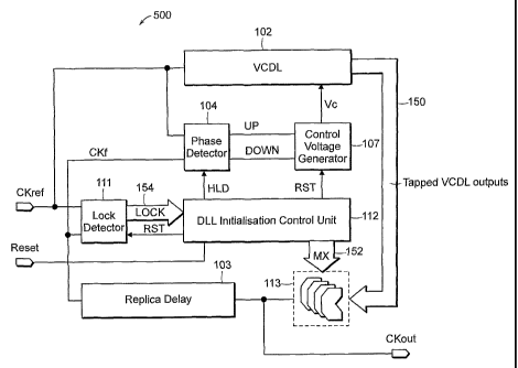
Fig. 5 is a block diagram of an embodiment of a Delay Lock Loop (DLL) 500 that
includes a DLL Initialization control 112 for initializing the DLL 500 after
power-up or
reset according to the principles of the present invention. The DLL 500
includes a
Voltage Controlled Delay Line (VCDL) 102, Phase Detector (PD) 104, control
voltage
generator 107, and replica delay 103 as described in conjunction with the
prior art DLL
shown in Fig. 1. The DLL also includes a multiplexer 113, a lock detector 111
and a DLL
initialization control 112 used for initializing the DLL 500 after power-up or
reset.
A reference clock signal CKref is coupled to the 'input of the voltage
controlled
delay line (VCDL) 102, one of the two inputs of the phase detector (PD) 104
and the lock
detector 111. The VCDL 102 produces tapped phase shifted output clock signals
116,
each of which is a delayed version of the reference clock signal CKref. A DLL
output
clock signal CKout is selected through multiplexer 113 from the tapped VCDL
outputs
116 dependent on an MX Code 152 output from the DLL Initialization Control
112. The
output clock signal CKout is, for example, routed to various circuits on a
semi-conductor
chip through a buffering structure referred to as clock tree.
The feedback clock signal CKf is the version of the reference clock signal
CKref
delayed by the VCDL 102 and replica delay circuit 103. The feedback clock
signal CKf is
tapped at a terminal node of a branch of the clock tree. Alternatively it can
be obtained by
applying the output clock signal CKout to a replica of the clock tree branch,
referred to
here as the replica delay circuit 103. The feedback clock signal CKf is fed
back to the PD
104 and the lock detector 111. The replica delay circuit 103 also known as a
delay model
or a clock tree branch replica, reproduces all delays added to the CKout
signal by the
multi-stage buffering structure of the clock tree. The delays include all
propagation delays
through the logical gates and buffers and delays caused by parasitic impedance
of long
wires. The feedback clock signal CKf replicates the clock signals at the
terminal nodes of
clock tree branches. For example, in a semiconductor chip, the clock signals
at the
terminal nodes are applied to the clock inputs of synchronous blocks and they
are
normally synchronized with the reference clock signal CKref.
8
CA 02596258 2007-07-27
WO 2006/081668 PCT/CA2006/000143
The DLL input or reference clock signal CKref is coupled to the VCDL 102. The
VCDL 102 includes a chain of similar buffers with variable delay. The chain
can contain
tens or even hundreds of buffers. The delay produced by the VCDL 102 is
variable and
controllable through a variable control voltage Vc applied to each buffer in
the VCDL 102
through the control voltage generator 107.
At the beginning of the initialization process, the control voltage Vc is set
to a
boundary voltage level (end point), that is, to a voltage level at which the
delay of VCDL
102 is set to a minimum delay. The boundary voltage level can be for example,
the power
supply voltage or ground. The RST signal generated by the DLL Initialization
Control
112 is coupled to the Control Voltage Generator 107 to set the initial control
voltage Vc.
The setting of the initial control voltage Vc can be for instance performed by
shorting the
Vc node to either power supply node (rail) or ground through a single-
transistor switch.
The phase detector 104 generates variable width pulses on the UP and DOWN
output signals dependent on the phase difference between the reference clock
signal CKref
and the feedback clock signal CKf. Both clock signals are coupled to the
inputs of the
phase detector 104. The variable width pulses on the UP and DOWN output
signals from
the phase detector 104 are integrated by the control voltage generator 107 in
order to
provide the Direct Current (DC) mode control voltage Vc. In one embodiment,
the control
voltage generator 107 can include a charge pump 105 and loop filter 106 as
described in
conjunction with the DLL 100 in Fig. 1. The control voltage generator 107
integrates the
PD output signals (UP, DOWN) by applying filtering and voltage level shifting
operations
as is well-known to those skilled in the art. Embodiments of VCDLs will be
described
later in conjunction with Figs. 7 and 8
Co-pending U.S. patent application entitled "High Output Impedance Charge
Pump for PLL/DLL," by Dieter Haerle (U.S. Patent Application No. 60/528,958),
the
contents of which are incorporated herein by reference in its entirety
describes an
embodiment of a charge pump in a control voltage generator. Another example of
charge
pump can be found in "A 2-1600MHz 1.2-2.5V CMOS Clock Recovery PLL with
Feedback Phase-Selection and Averaging Phase-Interpolation for Jitter
Reduction," Patrik
Larsson, 1999 IEEE ISSCC, WA 20.6, 0-7803-5129-0/99, Fig. 20.6.3, the contents
of
which are incorporated herein by reference in its entirety.
The phase detector 104 can be any phase detector that produces output signals
(UP,
DOWN) that are proportional in an electrical characteristic (for example,
voltage level or
9
CA 02596258 2007-07-27
WO 2006/081668 PCT/CA2006/000143
pulse width) to the phase difference between the clock signals applied to the
inputs
(CKref, CKf). Phase Detectors are well-known to those skilled in the art and
beyond the
scope of the present invention. Examples of Phase Detectors are described in
"An All-
Analog Multiphase Delay-Locked Loop Using a Replica Delay Line for Wide Range
Operation and Low-Jitter Performance," Yongsam Moon et al., JSSC Vol. 35, No.
3,
March 2000, pp 377-384, incorporated herein by reference in its entirety.
The ability to vary the delay produced by the VCDL 102 is used by the DLL 100
to
synchronize the reference clock signal CKref and the feedback clock signal CKf
by
aligning their respective rising edges. The control voltage Vc determines the
delay to be
added to the reference clock signal CKref by the VCDL 102 to align rising
edges of the
feedback clock signal CKf and the reference clock signal CKref.
The reference clock signal CKref and the feedback clock signal CKf are also
coupled
to the inputs of the lock detector 111. The lock detector 111 evaluates mutual
positioning
of the rising edges of the input clock signals (CKref, CKf) and generates a
LOCK
indication signal 154 that is indicative of the timing difference between the
rising edges of
the two clock signals. The LOCK indication signal 154 can be a single-bit
signal or a
multi-bit code. The internal structure and operation of an embodiment of the
lock detector
111 will be discussed later in conjunction with Fig. 9.
The multiplexer 113 is any suitable type of multiplexer known in the art that
selects one of a number of input signals (tapped VCDL outputs 116 in this
description) to
be transmitted to its single output (Ckout in this description) according to
the value of a
multi-bit code (MX 152). The tapped VCDL outputs will be described later in
conjunction
with Figs. 7 and 8.
The DLL initialization control 112 manages the initialization process, and is
responsible for maintaining the proper sequence of the initialization process.
The DLL
initialization control 112 also selects appropriate values for codes (MX 152)
and signals
(HLD, RST) based on the LOCK indication signal 154 received from the lock
detector
111.
After power up or reset, the DLL Initialization control 112 asserts the RST
signal
to reset the lock detector 111 and the control voltage generator 107. The
control voltage
Vc output from the Control Voltage Generator 107 is set to the voltage level
that provides
the minimum VCDL delay. The DLL Initialization Control 112 also asserts the
HLD
Signal coupled to the phase detector 104. While the HLD signal is asserted,
the, phase
CA 02596258 2007-07-27
WO 2006/081668 PCT/CA2006/000143
detector 104 can only increase the delay of the VCDL 102 by generating the
appropriate
UP/DOWN signals. Upon detecting from the state of the lock indication signal
154 that
the operating point is close to a first lock point, the DLL Initialization
Control Unit 112
outputs the appropriate MX code 152 to switch the phase of the output clock
signal
CKout. After the phase has been switched, the phase detector 104 continues to
increase
VCDL delay by modifying the control voltage Vc through generating the
appropriate
UP/DOWN signals until the next lock point is reached, as indicated by the lock
indication
signal 154.
The multiplexer 113 has multiple inputs and a single output. The MX code 152
selects one of the tapped VCDL output signals to be passed through to the
single output.
Only one tapped VCDL output signal can be passed to the multiplexer output at
a time, the
one that corresponds to the current value of the MX code. There is a limited
number of
delay stages between the adjacent tapped VCDL outputs, thus, the multiple
tapped VCDL
outputs create a "phase grid" in which the phase difference between two
adjacent tapped
signals is relatively small, a fraction of the clock signal period. With the
small phase
difference between the adjacent taps, a relatively large number of taps must
be skipped in
order to produce a larger phase shift. Thus, the complements of the tapped
VCDL signals
are used if the required phase shift at the output of the multiplexer is close
to 180 degrees
(big hop) and if needed more precise adjustment may be performed afterwards
using the
small phase difference between taps (smaller hops).
After the next lock point is reached, the initialization process is complete.
The
DLL initialization unit 112 de-asserts the HLD signal and the phase detector
104 can
increase or decrease the delay of the VCDL 102 during normal operation of the
DLL.
Thus, the DLL Initialization Control unit 112 controls the initialization
process so
that the VCDL delay starts at the minimum delay, the delay increases to the
first lock
point, the first lock point is skipped and the delay is further increased
until the DLL 500 is
locked at the second lock point. Further details of the operation of the DLL
initialization
control unit 112 will be discussed later in conjunction with Fig. 11.
Fig. 6A is a graph illustrating the initialization process on the control
voltage vs.
delay characteristic using the DLL 500 shown in Fig. 5. Fig. 6B is a clock
signal diagram
corresponding to the initialization process shown in the characteristic in
Fig. 6A. Figs. 6A
and 6B will be described in conjunction with Fig. 5.
11
CA 02596258 2007-07-27
WO 2006/081668 PCT/CA2006/000143
The control voltage Vc is initially reset to a boundary voltage level, that
is, to the
voltage corresponding to the smallest delay produced by the VCDL 102. The
boundary
voltage level can be for example, the power supply voltage or ground.
After reset or power-up, as the control voltage Vc is increased based on the
UP/DOWN signals output from the PD 104, the Voltage Controlled Delay Line
(VCDL)
102 starts increasing delay in direction 600 from the minimum delay point 602
(the left-
most point on the delay vs. control voltage characteristic) shown in Fig. 6A.
At the start of the initialization process, the lock detector 111 evaluates
the relative
positions of the rising edges of the two clock signals (CKref, CKf). Based on
the
evaluation, the lock detector 111 produces a LOCK signal 154 which is
indicative of the
proximity of the two clock signal rising edges. In one embodiment, the LOCK
signal 154
is a multi-bit code. The LOCK signal is received by the DLL Initialization
Control Unit
112. The DLL initialization control unit 112 generates a multi-bit output
selection code
MX 152 based on the value of the LOCK signal 154. The output selection code MX
152
is used to select one of the tapped phase-shifted output signals 116 received
from the
VCDL 102.
The delay through the VCDL 102 is gradually increased in one direction from
the
minimum delay point 602. During initialization, a HLD signal output from the
DLL
Initialization Control unit 112 and coupled to the PD 104 is asserted to hold
the PD 104 in
an initialization state. While in the initialization state, the PD produces
only an UP or a
DOWN signal so that the VCDL delay is only increased by appropriate
modification of
the control voltage Vc. The initialization process continues until the rising
edges of the
reference clock signal CKref and the feedback clock signal CKf are aligned
with a pre-set
degree of proximity. The degree of proximity is set to be substantially less
than half of the
period of the reference clock signal CKref.
After detecting that the rising edges of the reference clock signal CKref and
the
feedback clock signal CKf are aligned to the selected degree of proximity, the
output clock
signal CKout is inverted (that is, shifted 180 degrees for a 50% duty cycle
clock signal)
through appropriate selection of the output selection code MX 152 by the DLL
initialization control unit 112. Thus, the first lock point 604 is skipped.
The HLD signal
controlled by the DLL Initialization Control Unit 112 continues to hold the PD
104 in the
initialization state resulting in continued increase of the VCDL delay.
12
CA 02596258 2007-07-27
WO 2006/081668 PCT/CA2006/000143
After the first lock point 604 has been skipped, the DLL 500 continues
increasing
the delay by gradually increasing the control voltage Vc, until an accurate
alignment of the
rising edges of the reference clock signal CKref and the .feedback clock
signal CKf is
reached. The accurate alignment is indicated either by the LOCK signal 154 or
by the
state of the PD 104 UP and DOWN output signals. If PD 104 is used as the fine
alignment
indicating device in the initialization process as mentioned in previous
sentence, PD 104
can have a pair of separate UP and DOWN outputs dedicated for the
initialization and not
coupled to the inputs of the control voltage generator 107. Depending on PD
104 scheme
this might be necessary because UP and DOWN outputs connected to the inputs of
the
control voltage generator 107 may be disabled during initialization.
After the second lock point 606 is reached, the state of the HLD signal is
switched
to de-asserted to allow normal operation of the PD 104. The DLL 500 is then
allowed to
increase or decrease the VCDL delay as needed. By releasing the PD 104, the
initialization process is terminated and normal operation of the DLL is
enabled.
In one embodiment, the lock indication signal 154 is a multi-bit lock code.
The
multi-bit LOCK code 154 allows the DLL 500 to quickly move towards the desired
lock
point by selecting the tapped VCDL output 116 that corresponds to the desired
lock point
606. This allows the second (desired) lock point 606 to be reached quickly,
without
having to wait for the control voltage Vc to be gradually changed. In an
alternate
embodiment, the LOCK signal 154 is a single bit.
Fig. 7 is a block diagram of a single-ended embodiment of the VCDL 102 shown
in Fig. 5. The VCDL 102 includes a plurality of single-ended buffers 115
connected in
series to provide a delay line. Each buffer 115 has a single-ended input and a
single-ended
output. The single ended output of one buffer 115 is coupled to the single-
ended input of
a subsequent buffer in the VCDL 102. The control voltage Vc is supplied
directly to each
buffer 115 and determines the delay time produced by each buffer. Connection
of the
control voltage Vc to each buffer 115 is not shown in Fig. 7 for simplicity.
In this
embodiment, the VCDL output signal 117 is also single-ended. The inverted
version
(shifted by 180 degrees for a 50% duty cycle clock) of the VCDL output signal
117' is
provided through the output of an inverter 109, the input of which is coupled
to the VCDL
output signal 117.
Intermediate delayed versions of the reference clock signal CKref are obtained
by
tapping outputs of a group of buffers 114. The plurality of taps 116
constitute the tapped
13
CA 02596258 2007-07-27
WO 2006/081668 PCT/CA2006/000143
VCDL outputs 116 shown in Fig. 5. Each tap 116 is a delayed or phase-shifted
version of
the reference clock signal CKref. In different embodiments of present
invention the
VCDL 102 can output a plurality of tapped outputs 116 or a single output
signal 117 with
or without its respective complement 117'.
Fig. 8 is a block diagram of a differential-ended embodiment of a VCDL 102. In
this embodiment, the VCDL 102 includes a plurality of differential buffers 11
5a controlled
by control voltage Vc that is coupled to each differential buffer 115a (not
shown for
simplicity). The differential buffers 115a are connected in series. In this
embodiment,
differential buffers 115a have differential inputs and differential outputs.
The first buffer
11 5b has a single ended input for receiving the single-ended reference clock
signal CKref
and a differential output. The differential-ended embodiment of the VCDL 102
tends to
have better noise immunity than the single-ended embodiment of the VCDL. Also,
the
VCDL output 117a and every tapped output 116a has both the signal and its
complement.
With the complement of each tapped output signal provided, there is no need
for the
inverter 109 shown in the single-ended embodiment in Fig. 7. VCDL 102 can have
either
a plurality of tapped differential outputs 11 6a or a single differential
output 11 7a.
Fig. 9 is a schematic of an embodiment of a lock detector 111. The lock
detector
111 provides a lock indication signal (LC) 154 that indicates how close the
DLL is to a
lock point based on the phase difference between the reference clock signal
CKref and the
feedback clock signal CKf. Each stage 118 in the lock detector 111 receives
two clock
signals (CKref, CKf) at the input and outputs a single-bit LOCK signal (LC)
indicative of
the time difference between the rising edge of one of it's input clock signals
and rising
edge of it's other input clock signal.
Each stage 118 is a self-containing unit that includes two flip-flops 11 9a,
11 9b and
three delay lines 122a, 122b, 122c. Each of the delay lines 122a, 122b, 122c
has a
respective delay time interval (T1, T2) that is embedded in the delay line. In
the simplest
implementation, the lock detector 111 has a single stage 118 that outputs a
single bit lock
indication signal.
Fig. 10 is a timing diagram illustrating signals in one of the stages of the
lock
detector 111 shown in Fig. 9. Fig. 10 will be used in conjunction with Fig. 9
to explain the
operation of the lock detector 111. The position of the rising edges of the
reference clock
signal CKref and the position of the rising edges of a delayed reference clock
signal
CKref del are assumed to be stable. The timing diagram illustrates the
movement of the
14
CA 02596258 2007-07-27
WO 2006/081668 PCT/CA2006/000143
rising edge of the feedback clock signal CKf from left to right, from an
"early" ('E')
position to a "late" ('L') position. The E position is prior to the rising
edge of the
reference clock signal CKref and the L position is after the rising edge of
the delayed
reference clock signal CKref del.
Referring to Fig. 9, in each stage 118, the input clock signal CKref of the
stage 118
is delayed by delay line 122c having a delay time Tl. The delayed input clock
signal
CKref del is coupled to the "D" input of flip-flops 119a, 119b. The clock
input of flip-
flop 11 9a is coupled to the feedback clock signal CKf. The clock input of
flip-flop 119b is
coupled to a delayed feedback clock CKf del that has been delayed through
delay line
122a having a delay time interval of Tl and delay line 122b having a delay
time interval of
T2. The delay lines 122a, 122b are connected in series.
The delay time intervals Tl and T2 are embedded in the delay lines 122a-c, and
can be same value or different. The delay time intervals can also be modified
depending
on the application. In general, the lock detector 111 includes a plurality of
stages 118 of
similar structure as described in conjunction with Fig. 9. However, for
different
implementations, stages 118 can differ in the Tl and T2 delay values embedded
in the.
delay lines 122a-c. The preferred value for both T1 and T2 is a fraction of
the period of
the reference and feedback clock signals (CKref, CKf), with the fraction being
smaller
than a quarter of the clock period at the highest clock signal frequency. In
some
embodiments, the delay time interval is shorter than a half of the delay time
between two
adjacent VCDL taps 116, 116a. For other embodiments, the delay time interval
is slightly
longer than half of the delay time between two adjacent VCDL taps 116, 116a.
In the embodiment shown, delay time intervals T1 and T2 are different. If the
rising edge of feedback clock signal CKf is expected to "approach" the rising
edge of the
reference clock CKref during initialization from one side (e.g., left of fig.
6 timing
diagram), delay time interval T2 "opens the lock window" and delay time
interval T1
constitutes the margin for the lock detector. Generally, Tl and T2 are
different values. In
this example typically, delay time interval Tl is selected to be less than
delay time interval
T2, to ensure "early warning" that the lock point is approaching and tighter
control on the
other side of the lock point.
Typically, delay time intervals (Tl, T2) are short because it takes
significant
silicon area overhead to obtain longer delays. However, the delay time
intervals cannot be
CA 02596258 2007-07-27
WO 2006/081668 PCT/CA2006/000143
too short because the LC signals 154 need to stay stable during a number of
clock cycles
while the VCDL delay is adjusted by the- DLL 500.
Referring to the schematic in Fig. 9, when the rising edge of the feedback
clock
signal CKf is in the "E" position, the rising edge of the feedback clock
signal CKf is early
with respect to the reference clock signal CKref. The LC signal 154 is '0'
because the ER
signal at the output of inverter 120 is '1' and the LT signal at the Q output
of flip-flop
119b is '0'.
The ER and LT signals are combined by AND logic gate 121 to provide LC signal
at the output. The combination of a'0' on the LT signal and a'1' on the ER
signal, results
in a'0' on the LC signal at the output of AND logic gate 121.
As the VCDL delay is increased, the feedback clock signal CKf rising edge
moves
towards the right and reaches the "i" position. The LC signal switches to '1'
because the
both the 'ER' signal and the 'LT' signal are ' 1' .
Referring to the schematic, the delayed feedback clock signal CKf del also
reaches
its respective "i" position. At the rising edge of the delayed feedback clock
signal
CKf del, the delayed reference clock signal CKref del is '1' and the '1' on
the D input of
flip-flop is latched to the Q output of flip-flop 119b. The combination of a'
1' on the LT
signal and a' 1' on the ER signal, results in a' 1' on the LC signal at the
output of AND
logic gate 121'.
The LC signal remains at '1' while the position of the rising edge of the
feedback
clock signal CKf continues to move to the right in example of Fig. 10 until
the rising edge
reaches the "ii" position. At the 'ii' position, the delayed reference clock
CKref del is '1'
because the D input of flip-flop 11 9a is '1', the next rising edge of the
feedback clock CKf
clocks a' 1' to the Q output of flip-flop 11 9a and the ER signal at the
output of inverter
120 switches to '0'. The combination of a'1' on the LT signal and a 01' on the
ER signal,
results in a' 1' on the LC signal at the output of AND logic gate 121'.
The state of the LC signal provides an indication of the time between the
rising
edge of the feedback clock CKf and the rising edge of the reference clock
CKref. The LC
signal remains '1' while the rising edge of the feedback clock signal CKf is
within time T2
and T1 from the rising edge of the CKref clock signal, that is, between
position (i) and (ii).
If a plurality of stages 118 are included in the lock detector 111 and each
stage
receives the same feedback clock signal CKf and a different tap 116 of the
reference clock
signal CKref from the VCDL 102, the tap of the reference clock CKref whose
rising edge
16
CA 02596258 2007-07-27
WO 2006/081668 PCT/CA2006/000143
is closest to the rising edge of the feedback clock signal CKf can be easily
identified. One
method is to let the DLL continue to advance the rising edge of the feedback
clock CKf ,
that is, increase the VCDL delay by gradually changing the control voltage Vc
value and
monitor which of the plurality of LC signals switches to '1'.
Another method is to monitor both the ER and LT signals directly instead of
the
LC signal. The combination of the ER and LT signals provides four possible
states (00,
01, 10 and 11). The state is '10' (the ER signal is '1' and the LT signal is
'0) when the
rising edge of the feedback clock signal CKf is more than T2 earlier than the
rising edge
of the reference clock signal CKref. The state is '01'(the ER signal is '0'
and the LT
signal is '1') when the rising edge of the feedback clock CKf is more than Tl
later than
the rising edge of the reference clock signal CKref. Thus, if the rising edge
of a feedback
clock CKf is later then the rising edge of the reference clock CKref at the
VCDL tap 116,
116a with order number "N", but the rising edge of the feedback clock signal
CKf is
earlier than the rising edge of the reference clock signal CKref at the next
tap 116, 116a
with order number "N+l", the state (ER and LT signal combination) at tap "N"
is "11" or
"01" and the state (ER and LT signal combination) at tap "N+1" is "10" or
"11". If values
Tl and T2 are both chosen as a small portion of the time delay between
adjacent taps, for
example, one tenth of the time delay between the two adjacent taps N, N+1, the
"11"
combination is never present at two adjacent taps simultaneously and it is
easy to see that
the lock point (state '11') is between the two taps.
The method using only a single LC signal output from each stage 118 is simpler
to
implement than the method using the ER and LT signals. However, the method
using the
combination of the ER and LT signals is a faster method for bringing the DLL
to a lock
point. One skilled in the art will understand that in an alternate embodiment,
a
combination of all three signals: LC, LT and ER can also be used to initialize
the DLL
operating point.
Returning to Fig. 5, the DLL initialization control 112 controls the
initialization
process. The initialization control 112 is a state machine. The process
includes choosing
the correct values for applied signals (RST, HLD, MX) during the DLL
initialization
process. Those skilled in the art understand that there are many ways to
implement or
synthesize a state machine. Therefore an algorithm used for synthesizing the
state
machine with the desired functions of the DLL initialization control 112 is
described
rather than a schematic or elements of the internal structure of the DLL
initialization
17
CA 02596258 2007-07-27
WO 2006/081668 PCT/CA2006/000143
control itself. It is also noted that the algorithm discussed here and
represented in Fig. 11
is not the only logical scheme that can be used to implement the
initialization process.
The sequence of the steps can be changed and steps can be added, removed or
modified.
Fig 11 is a flowchart illustrating the DLL initialization process implemented
in the
DLL initialization control 112. The DLL initialization process starts each
time a power up
or system reset occurs. Fig. 11 will be described in conjunction with Fig. 9
and Fig. 5.
At step 200, referring to Fig. 5, the system Reset signal (not shown for
simplicity)
is coupled to the DLL 500 and to various modules within the DLL 500. The RST
signal is
input to the lock detector 111 and the control voltage generator 107. The RST
signal
resets the lock detector 111, if necessary. For example, the reset signal can
reset the lock
detector 111 when coupled to the clear inputs of flip-flips 119a, 1 19b by
clearing both
flip-flops 11 9a, 11 9b shown in Fig. 9 so that the respective Q output of
each flip-flop is set
to V. The reset signal also discharges the control voltage node Vc to the
boundary value,
that is, the value that produces minimum delay. The reset signal also asserts
the HLD
signal to a "hold" mode, sets the initial value for the MX control code 152
and the desired
degree of proximity for the searched lock point.
At power up, the MX code value 152 is set to the initial value so that the
VCDL
tapped output 116 or 116a with minimum phase shift (left most tapped output
(phase 1)
shown in Figs. 7 and 8) is selected. The desired lock proximity degree is set
by selecting
the lock detector I11 instead of the PD 104 as the device to evaluate the
degree of
proximity of the rising edges of the clock signals (CKref, CKf).
The value of the MX output 152 from the DLL Initialization Control 112 at
power
up can differ depending on the implementation. The MX output 152 can be either
single
or multi-bit. In the embodiment shown in Fig. 5, MX is a multi-bit code.
Single and
multi-bit implementations will be discussed later. While the HLD signal is set
to "hold",
the PD 104 is in "hold mode" and the PD 104 controls the UP and DOWN output
signals
so that the VCDL 102 delay can only be increased. While the PD 104 is in "hold
mode",
its separate dedicated output signals can still be used to measure with higher
accuracy the
proximity of the rising edges of the input clock signals (CKref, CKf).
Even the most accurate Phase Detector registers the edge alignment with a
certain
finite accuracy. This accuracy among other factors determines the accuracy of
the DLL
clock alignment. For example, if the PD error is 20ps and the DLL is in steady
lock, clock
edges are within 20ps from each other, other factors excluded. The PD output
signals
18
CA 02596258 2007-07-27
WO 2006/081668 PCT/CA2006/000143
therefore indicate alignment of the clock edges when the time difference
between the
clock edges is 20ps or less.
The initialization of the DLL starts with the minimum VCDL 102 delay and the
delay can only be increased. Returning to Fig. 11, at step 202, the clock
(CKref, CKf)
advances one cycle (that is, one clock period) and the alignment of the rising
edges of the
clocks (CKref, CKf) in the respective clock cycle is measured by the lock
detector 111
and/or PD 104 as previously discussed.
At step 204, the DLL Initialization Control 112 determines if the lock has
been
found with the desired degree of proximity based on the LOCK code 154 (Fig. 5)
forwarded from the lock detector 111 (Fig. 5). The lock proximity degree is
the accuracy
to which the lock point is found. The lock proximity degree is stored in the
DLL
initialization Control 112 as a loadable code in a register or a fuse
programmed code. The
lock proximity degree is used to set values for the Tl and T2 time intervals
in the lock
detector 111.
The lock detector 111, as previously discussed, can either determine a rough
alignment or an accurate alignment, that is degree of proximity (rough or
accurate) of the
rising edges which is determined by the T1 and T2 time interval values
settings and
whether the ER, LT, LC signals or their combination is used to select the lock
point.
The alignment accuracy can vary during the DLL initialization process. In the
beginning of the initialization process it is sufficient to detect alignment
roughly. The
rough alignment is typically performed by the lock detector 111 as described
in
conjunction with Figs 9 and 10. At the start of the DLL initialization
process, when
approximate edge alignment is satisfactory, lock detector stages 118 with long
T1 and T2
time intervals and a simple LOCK code are used. When more accurate alignment
is
required, shorter Tl and T2 time intervals and a more complex combination of
ER, LT and
LC signals in the LOCK code is used. Alternatively, PD 104 can engage at this
stage as
the edge alignment detector.
Continuing the initialization process: at each rising clock edge DLL evaluates
the
degree of proximity (alignment) between the rising edges of the clock signals
and
produces corrective signals. The control voltage Vc is constantly modified
based on the
values of UP, DOWN signals from the phase detector 104.
19
CA 02596258 2007-07-27
WO 2006/081668 PCT/CA2006/000143
After a few initial clock cycles, the LOCK code settles indicative of DLL
approaching the first lock point. After the first lock point has been reached
with the
desired degree of proximity, process continues with step 206.
At step 206, the first lock point is skipped by modifying the IVIX code so
that the
phase of the feedback clock signal CKf is shifted through the multiplexer 113.
The VCDL
delay can also be increased quickly by performing a phase shift after only a
very few clock
cycles immediately following power up or reset. In this case an accurate lock
detector with
high granularity VCDL tapping is used which allows for fast and accurate
location of the
first and second lock points 604, 606 which in turn allows the value of MX
code
corresponding to the second lock point to be produced quickly.
Referring to the timing diagram of Fig. 6B and graph of Fig. 6A, after having
reached and skipped the first lock point 604, the delay continues to be
increased by
modifying the value of the control voltage Vc so that DLL moves towards the
next,
second lock point 606. The delay is initially increased quickly by shifting
the phase, the
delay is then increased gradually, by modifying the control voltage Vc
gradually - a
relatively small change on each clock cycle. The timing diagram also shows
that the
second lock point 604 is reached by gradually increasing the VCDL delay.
Gradually
changing the value of the control voltage Vc is slower than a phase-shift,
however it still
increases the VCDL delay and allows the DLL to reach the control voltage Vc
value
corresponding to the second lock point.
The DLL can be brought to the final lock point (for example, second lock point
606) in single phase-shift with the control voltage Vc set to a value
corresponding to the
VCDL minimum delay. To perform this operation, a tap 116, 116a is selected so
that the
DLL skips the first lock point and lands very closely to the second lock point
with Vc held
to produce minimum delay. However, after Vc is released as operation
conditions change,
the DLL will not have much room for decreasing the delay, because the control
voltage Vc
is not too far from the value that produces minimum delay. Thus, the DLL will
easily lose
lock should significant delay decrease be required to compensate for drift of
clock signals
edges and change of operation conditions.
The part of VCDL delay increase achieved before the final lock due to the Vc
voltage level modification only needs to be greater or at least equal to the
maximum
VCDL delay decrease required during DLL normal operation (range 304 in Fig.
3B) plus
some safety margin. Obviously, choosing a longer timing interval will make the
search
CA 02596258 2007-07-27
WO 2006/081668 PCT/CA2006/000143
for the final lock longer too. However, as already discussed, the timing
interval is
determined by maximum VCDL delay modification (decrease) that might be needed
at
any time during normal DLL operation under influence of the clock signals
edges drift and,
change in operating conditions.
In one embodiment, the lock detector 111 includes a plurality of stages 118
with
only the LC outputs of each respective stage 118 used in the lock detector 111
output
LOCK code. The stages 118 in this embodiment have different values of the Tl
and T2
delay times embedded in their respective delay lines 122a-c. The delay lines
122a-c in
this case are replicas of portions of the VCDL 102 buffer chain 114. The first
stage 118a
has' a smaller number of the buffers in delay lines 122a-c and the LC signal
of the next
stage is asserted (set to logic '1') when rising edges of the reference clock
signal CKref
and the feedback clock CKf are closer to each other.
Each next stage 11 8b has more buffers compared to the previous stage. Thus,
the
degree of proximity in each next stage 11 8b is less accurate (rougher) and
the respective
LC output is asserted (set to logic '1') when the rising edges of the clock
signals (CKref,
CKf) are further away from each other. The combined LC outputs from all
stages, that is,
the LOCK output code of the lock detector 111 in this embodiment. The LOCK
code is
indicative of how many single VCDL buffers need to be added to the reference
clock
signal CKref path in the VCDL in order to bring rising edges of the clock
signals CKref
and CKf close to each other. In other words, the LOCK output code 154
identifies the tap
to be selected from the tapped VCDL outputs by the MX code 152 in order to
skip the first
lock point 604 to bring the DLL operating point close to the second lock point
606.
Thus, at step 208, the DLL initialization control 112 changes the desired
proximity
degree to accurate by asserting the MX code value that corresponds to the
second lock
point and by switching to PD 104 control. At this stage of the initialization
process, the
dedicated UP and DOWN signals are used to evaluate clock rising edge
positioning with
high accuracy while UP and DOWN outputs are still held by the HLD signal in
order to
still only increase the VCDL 102 delay. Alternatively, the lock detector 111
can remain in
control while the PD 104 is held to produce UP and DOWN output signals to
increase the
VCDL 102 delay time.
At step 210, the clock (CKref, CKf) advances one cycle. The next rising edges
of
the reference clock signal CKref and the feedback clock signal CKf are
detected and the
degree of proximity is measured.
21
CA 02596258 2007-07-27
WO 2006/081668 PCT/CA2006/000143
At step 212, if the second lock point has been reached with a desired degree
of
proximity, process continues with step 214. If not, process continues with
step 210 to
continue to monitor the degree of alignment between the reference clock signal
CKref and
the feedback clock signal Ckf.
At step 214, the more accurate final lock is reached, and the PD 104 is
released by
switching the HLD signal to "release" state.
At step 216, the PD 104 controls the control voltage Vc and normal DLL
operation
begins.
Other embodiments of a DLL are shown in Figs. 12 -15.
Fig. 12 is a block diagram of an alternate embodiment of a DLL 140 including
DLL initialization according to the principles of the present invention. This
embodiment
is more suitable for cases where faster DLL initialization is required, that
is, when the time
needed for reaching the final DLL lock point and switching to normal DLL
operation is
critical.
The DLL 140 has many common elements with the embodiment of the DLL 500
described in conjunction with Fig. 5. The DLL includes a VCDL 102 having a
plurality of
tapped outputs 116 or 116a, a PD 104, a control voltage generator 107, a
multiplexer 113,
and a DLL initialization control 112 as discussed in the embodiment shown in
Fig. 5. In
contrast to the single replica delay 103 in the DLL 500 shown in Fig. 5, DLL
140 includes
a plurality of replica delay blocks 103, with one replica delay block 103 for
each of the
VCDL 102 tapped outputs 116 or 116a.
The lock detector 111 has an internal structure as shown in Fig. 9, with a
plurality
of stages 118 equal in number to the number of the VCDL tapped outputs 116 or
116a.
Both timing intervals Tl and T2 in all stages 118 are set to same value. The
value of the
timing interval Tl, T2 is much smaller than the delay time between two
adjacent VCDL
taps 116 or 116a. The LOCK code output by the lock detector 111 includes LC,
LT and
ER outputs of all stages 118. This allows for higher accuracy in determining
mutual
positioning of the clock signals' rising edges. Two multiplexers 113a-b are
used:
multiplexer 113a for selecting the DLL output clock signal from a number of
VCDL 102
tapped outputs and multiplexer 113b for selecting the feedback clock signal
CKf. Both
multiplexers 113a-b are controlled by the same MX multi-bit code. In
comparison to the
embodiment described in conjunction with Fig. 5, additional silicon area
overhead is
needed to accommodate the two multiplexers 113a-c, the plurality of replica
delays 103
22
CA 02596258 2007-07-27
WO 2006/081668 PCT/CA2006/000143
and the clock detector stages 118 in the lock detector 111 to provide the
higher accuracy
and faster time to lock.
Clock signals from tapped VCDL outputs 116 or 11 6a are forwarded to the
replica
delays 103 and to the first multiplexer 113a. After having passed through the
replica
delays 103, the clock signals are forwarded to lock detector 111 and the
second
multiplexer 113b. The DLL initialization control 112 controls the
initialization process
described in conjunction with Fig. 11. On power up or system reset, control
voltage
generator 107 resets control voltage Vc to the boundary value so that the VCDL
102
produces minimum delay. The reset signal shown in the embodiment in Fig 5 has
been
removed for simplicity. The state of the HLD signal value is set to "hold" to
hold the PD
104 in delay increasing mode, the lock detector 111 is reset and the MX multi-
bit code is
either set to a default value or left at an initial random value at this time.
The desired degree of proximity is set by allowing the lock detector 111 to
control
the control voltage Vc and holding PD 104 in "hold" mode. After a few clock
cycles, the
LOCK code value stabilizes and indicates with high accuracy the phase
difference
between the clock signals CKref, DKf based on the position of the rising edges
of the
plurality of clock signals at the outputs of the replica delays 103 compared
to the rising
edge of the reference clock signal CKref. Using the LOCK code value received
from the
lock detector 111, the DLL initialization control 112 selects the closest
version of the
clock output from the VCDL 102 for the output clock signal CKout through
multiplexer
113 a and the respective version of the clock signal CKf output from the
replica delay unit
103 to feed back to PD 104 through multiplexer 113b.
In order to determine the value for the MX code, it is important to note that
the
versions of the clock signals selected by both multiplexers 113a, 113b relate
to the same
tapped output of the VCDL 102. Thus, the versions of the clock signals are
selected by
the MX code and the phase shift is performed almost directly after the reset
or power up.
After the phase shift, the operating point of the DLL is close to the second
lock point 606
(Fig. 6A) and the DLL initialization control 112 gradually increases the
control voltage Vc
through the PD 104 while the HLD signal holds the outputs of the PD 104, so
that the PD
104 only increases the VCDL delay. The increase in control voltage Vc
continues until
the second lock point 606 (Fig. 6A) is reached. After the second lock point
606 (Fig. 6A)
is reached, the DLL initialization control 112 changes the state of the HLD
signal to
"release" and the desired lock proximity degree is switched to "accurate" by
transferring
23
CA 02596258 2007-07-27
WO 2006/081668 PCT/CA2006/000143
control of the control voltage Vc to the PD 104. Normal operation of the DLL
starts.
Even in this "lock accelerated" embodiment DLL can not be brought exactly to
the second
lock point by the phase shifting only while Vc remains at the value
corresponding to
miniinum delay. As discussed above, the margin is needed for VCDL delay
variation
compensating for clock edge drifts and operation condition change. Therefore
the phase
shift brings DLL to the second lock point as close as the margin and the rest
of the way
(the margin) is covered by gradually modifying Vc.
The embodiments of the DLL shown in Figs. 13-15 include an inverting unit 110
that is not used in the embodiment of the DLL previously described in
conjunction with
Fig. 5 or in the prior art DLL described in conjunction with Fig. 1.
Referring to Fig. 13, in the simplest case, the inverting unit 110 includes an
inverter 109 and multiplexer 108. The function of the inverting unit 109 is to
split an
input signal into an inverted and non-inverted version and to select one of
the versions to
be supplied to the output according to the logical value of a single-bit MX
signal. For
example, when the MX signal is '0', the non-inverted version of the signal is
output, when
the MX signal is '1' the inverted version of the signal is output or vice
versa. Therefore,
the inverting unit 110 is similar to the multiplexer 113 that has previously
been described
in conjunction with the embodiment shown in Fig. 12.
As is well-known to those skilled in the art, there are many possible ways to
implement the function of the inverting unit 110. As the inverting unit 110 is
not a subject
of this invention, these are not discussed here. Any variant can be chosen as
long as the
unit function is provided. One skilled in the art will understand that the
internal structure
of the inverting unit 110 can be different from that shown in Fig. 13. For
example, the
inverting unit 110 can have a single ended or differential input and a
differential output
with phase or counter-phase output selected by the MX signal. The inverting
unit 110 can
also include an additional chain balancing delay of the two paths inside the
unit - inverting
and non-inverting. It is also understood that the inverter 109 may not be
necessary in the
inverting unit 110 in cases when the VCDL 102 output provides the signal and
complement pair 117a (Fig. 8) or signal and complement 117 and 117' (Fig. 7).
In this
case the inverting unit 110 includes a 2-input and 1-output version of the
multiplexer 113.
The embodiment of the DLL shown in Fig. 13 does not find the lock point as
quickly as the embodiment described in conjunction with Fig. 12. However, the
embodiment in Fig. 13 is simpler to implement and requires less silicon area
overhead.
24
CA 02596258 2007-07-27
WO 2006/081668 PCT/CA2006/000143
The DLL 142 includes only one VCDL output, one inverting unit 110 and a lock
detector 111 with only one stage 118. Alternatively, in the case when the VCDL
102
provides output signals and their complements 117a as shown in Fig. 8, the
inverting unit
110 can be replaced by a 2-input and single-output multiplexer 113. The timing
intervals
T1 and T2 in the lock detector 111 are set to a small fraction of the clock
period. The lock
detector 111 detects the lock point only when the rising edges of the
reference clock signal
CKref and the feedback clock signal CKf are close to each other.
The DLL initialization control 112 gradually increases the delay from the
initial
delay after reset or power-up. After the first lock point 604 (Fig. 6A) is
detected based on
the state of the lock signal, the inverting unit 110 switches to the inverted
clock based on
the MX signal output by the DLL initialization control 112 thus jumping over
the first lock
point. After the inverting unit 110 switches, the PD 104 is still held by the
HLD signal to
only increase the delay by increasing the control voltage Vc. The DLL 142
continues to
gradually increase delay by increasing the control voltage Vc based on the
time delay
between the rising edges of the reference clock signal CKref and the feedback
clock signal
CKf. After the second lock point 606 (Fig. 6A) is detected, the PD 104 is
released by
changing the state of the HLD signal and normal operation starts.
In the embodiments of the DLL shown in Figs. 14 and 15, the inverting unit 110
is
connected in a different location from the previously discussed embodiments.
Referring to Fig. 14, the DLL 144 includes two inverting units 110a, 110b. The
input of inverting unit 110a is connected to the output of the replica delay
103. The input
of inverting unit 110b is connected to the output of the VCDL 102. The output
of
inverting unit 1 l0a is a DLL output clock signal CKout. The output of
inverting unit 110b
is a DLL internal feedback clock signal CKf that is coupled to the input of
the PD 104 and
the input of the lock detector 111.
Referring to Fig. 15, DLL 146 includes one inverting unit 110 that is coupled
between the reference clock signal CKref and the input of the VCDL 102, that
is in the
reference clock signal CKref path.
Neither DLL 144 (Fig. 14) or DLL 146 (Fig. 15) shows a Reset signal or MX,
RST, HLD internal DLL signals. These signals were removed from the diagrams
for
simplicity. One skilled in the art will understand that all those signals are
present in the
system and applied in the same manner as they are applied in all previously
discussed
embodiments.
CA 02596258 2007-07-27
WO 2006/081668 PCT/CA2006/000143
One skilled in the art will recognize that DLL structures using the DLL
initialization process are not limited to those described. An experienced
designer can
design other DLL structures that will benefit from the ideas described here
with respect to
the DLL initialization process.
In other embodiments, a DLL searches for a lock point by starting from a point
of
the delay vs. control voltage characteristic close to the maximum delqy. The
direction of
the search for a lock point during initialization is restricted to delay
decrease only, that is,
a phase detector is forced to produce only a combination of UP and DOWN
signals that
corresponds to delay decrease, depending on internal structure of the phase
detector. In
one embodiment, the starting point is below the steep area corresponding to
maximum
delay in order to avoid this area. As the operating point will be below the
initial delay,
only some of the stages in the DLL might be used, others might be disabled
during
initialization.
While this invention has been particularly shown and described with references
to
preferred embodiments thereof, it will be understood by those skilled in the
art that various
changes in form and details may be made therein without departing from the
scope of the
invention encompassed by the appended claims.
26