Note: Descriptions are shown in the official language in which they were submitted.
CA 02597009 2007-08-07
WO 2006/081633 PCT/AU2006/000152
-1-
TITLE: WAVEGUIDE DESIGN INCORPORATING REFLECTIVE OPTICS
FIELD OF THE INVENTION
This invention relates to an improved design for the transmit and receive
optics
of a waveguide-based optical touch screen sensor. The improved design
incorporates
reflective optics, and has the advantages of reduced temperature sensitivity
and
reduced optical losses. However, it will be appreciated that the invention is
not
limited to this particular field of use, and may be applied to the coupling of
light
between any two optical elements, at least one of which is a waveguide.
BACKGROUND TO THE INVENTION
Any discussion of the prior art throughout the specification should in no way
be considered as an admission that such prior art is widely known or forms
part of
common general knowledge in the field.
Figure 1 illustrates the operation of an optical touch screen sensor 1
described
in US Patent Nos. 5,914,709, 6,181,842 and 6,351,260, and US Patent
Application
Nos. 2002/0088930 Al and 2004/0201579 Al (the contents of which are
incorporated
into this specification by way of cross-reference). In this optical touch
screen sensor
design, integrated optical waveguides 2, 3 are used to launch an array of
light beams 4
across a screen, then collect them at the other side of the screen and conduct
them to a
position-sensitive detector. A touch event 5 (eg. by a finger or stylus) is
detected as a
shadow 6, with position determined from the particular beam(s) blocked by the
touching object. The touch screen sensors are usually two dimensional and
rectangular, with two arrays (X, Y) of transmit waveguides along adjacent
sides of the
screen, and two corresponding arrays of receive waveguides along the other two
sides
of the screen. As part of the transmit side, in one embodiment a single
optical source
(such as a light emitting diode (LED) or a vertical cavity surface emitting
laser
(VCSEL)) launches light into a plurality of waveguides that form both the X
and Y
transmit arrays. In another embodiment, a separate optical source is used for
each of
the X and Y transmit arrays. In an existing design for the transmit side, the
waveguide
arrays guide light from the source to rows of lenses 7 that expand the guided
light
beams in the horizontal (ie. x,y) plane, then collimate them in the horizontal
plane as
they are launched across the screen face. Collimation in the vertical plane
may be
CA 02597009 2007-08-07
WO 2006/081633 PCT/AU2006/000152
-2-
achieved with an extemal vertical collimating lens (VCL), for example a
cylindrical
lens, not shown in Figure 1. The receive side is essentially identical, and on
each side
the arrays of waveguides and lenses are positioned within the bezel of the
screen.
US Patent Application No. 2004/0201579 Al teaches that the light beams
launched across the screen preferably form a "lamina" (ie. a thin sheet) of
light, and
more preferably a lamina of substantially uniform intensity. Compared to the
alternative of having discrete beams separated by considerable dark regions, a
lamina
of light minimises the required dynamic range of the photodetectors associated
with
the X, Y receive arrays, enhances the grey scale interpolation of the position
sensing
algorithms, and minimises the chance that a thin touching object could be
missed by
the beams. The discrete beam case also complicates the manufacturing process,
because the receive side waveguides need to be critically aligned (in the
horizontal
plane) with the transmit side waveguides; with a lamina of light, the
horizontal
positioning of the receive side waveguides is non-critical. Accordingly,
although an
optical touch screen sensor of this type can operate with discrete beams, it
is
preferable for the beams to approximate a lamina as closely as possible.
Figure 2 illustrates the operation of an optical transmission device 20 of a
type
described in US Patent Application No. 2002/0197010 Al, the contents of which
are
incorporated into this specification by way of cross-reference. The device 20
shown
in Figure 2 serves to couple light between two integrated optical waveguides
21 and
22, formed on separate substrates (not shown). It will be appreciated by those
skilled
in the art that since optical waveguides are typically small structures (of
order 10 m x
10 m), it is difficult to couple light between them efficiently without
resorting to
expensive active alignment schemes. It is therefore preferable to use some
sort of
beam expanding device such as that illustrated in Figure 2 to reduce the
alignment
tolerances. In the particular device shown in Figure 2, light 23 propagating
along
waveguide 21 is expanded and collimated in the horizontal (page) plane by
planar lens
24, formed integrally with waveguide 21, then collimated in the vertical plane
by
external cylindrical lens 25 to produce expanded beam 26. A similar pairing of
cylindrical lens 27 and planar lens 28 focuses the light into waveguide 22.
As disclosed in US 2002/0197010 Al, the basic design shown in Figure 2 can
be expanded to provide a multi-channel transmission device with a plurality of
input
CA 02597009 2007-08-07
WO 2006/081633 PCT/AU2006/000152
-3-
waveguides 21 and planar lenses 24 formed on a common substrate and a like
plurality of output waveguides 22 and planar lenses 28 formed on a second
common
substrate, with a single cylindrical lens 25 common to all input waveguides 21
and a
single cylindrical lens 27 conunon to all output waveguides 22. It will be
appreciated
that in such a situation, the optics of the devices shown in Figures 1 and 2
have many
similarities. In related transmission devices, waveguide 22 with its planar
lens 28 and
external lens 27 may be replaced by another optical element, such as an
optical source
or a detector.
For reasons of cost and ease of fabrication, it is highly preferred in many
optical waveguide applications to form the waveguides and/or associated lenses
out of
a photo-patternable polymer material. Polymers are known to have large thermo-
optic
coefficients, ie. the rate of change of refractive index with temperature
(dn/d.T), of
order -1 to -4 x 10"4/ C. These large dn/dT values can be used to advantage in
thermo-
optic devices such as switches, tuneable gratings and variable optical
attenuators (see
for example US Pat. No. 6,434,318, and "Advances in polymer integrated
optics", L.
Eldada and L.W. Shacklette, IEEE Journal of Selected Topics in Quantuin
Electronics
vol. 6, No. 1, pp. 54-68 (2000)). However in certain applications such as the
optical
touch screen sensor of Figure 1 and the transmission device of Figure 2, a
large dta/dT
is disadvantageous because modest variations in ambient temperature, say over
aii
operating range of -10 to 50 C, adversely affect the horizontal collimation at
the
planar lenses in Figures 1 and 2, by changing the angle of refraction at the
polymer/air
interfaces. This is because refraction is govemed by Snell's Law (n.; sin 8i =
nt sin Bt),
and a temperature-induced variation in one or both of the refractive indices
nt and nt
will change the angle of refraction B1, unless the angle of incidence B; is
zero (ie.
normal incidence). In the operation of an optical touch screen as shown in
Figure 1,
this dependence of refraction on temperature means that optics made of a
polymer
material and designed to launch collimated beams across the screen and receive
them
at the other side will only do so over a certain temperature range. If the
temperature
drifts too far, variations in the emission angles at the transmit side and/or
in the
3o acceptance angles at the receive side will reduce the collection
efficiency, representing
a source of optical loss in the system. Furthermore, stray light may be
collected by
adjacent receive lenses, possibly causing errors in determining the position
of a touch
CA 02597009 2007-08-07
WO 2006/081633 PCT/AU2006/000152
-4-
event. Similarly, if waveguides 21 and 22 and planar lenses 24 and 28 in the
transmission device shown in Figure 2 were composed of polymer, temperature
variations will affect the coupling efficiency between waveguides 21 and 22.
The
inventors of US 2002/0197010 Al consider the effects of temperature variations
on
the external cylindrical lenses 25 and 27, but they do not consider the
effects on planar
lenses 24 and 28, even though they are preferably composed of polymer
materials.
There exists then a need for a solution to this temperature sensitivity
problem.
One possible solution is to use a waveguide material with a mucll smaller
thermo-
optic coefficient, for example silica (dn/dT - +1 x 10⁻⁵/ C). However silica
glass
waveguides are much more expensive to fabricate, both in terms of fabrication
equipment and processing time, and are simply not an option for a mass-
produced
consumer electronics device such as an optical touch screen sensor. Another
possible
solution is to use a polymer with a thermo-optic coefficient at the low end of
the
polymer range, say around -1 x 10-'/ C. However this is still an order of
magnitude
greater than the thermo-optic coefficient of silica, so the temperature
sensitivity will
still be significant. Also, if a polymer has a low dn/dT, it is invariably
below its glass
transition temperature (Tg), ie. it is in its glassy state, and as expounded
in US Pat.
No. 6,236,774, for long term stability of polymer waveguides it is preferable
to
operate above Tg, in which case the dn/dT will be at the high end of the
polymer
range.
The transmit and receive lenses of the existing optical touch screen design
also encounter difficulties with collimation in the vertical plane, where for
ease of
assembly it is convenient to use a single VCL for all transmit or receive
lenses in each
array along the respective sides of the optical touch screen. The positioning
of the
VCL with respect to the curved end face 31 of a prior art transmit lens 30 is
shown in
Figures 3a (plan view) and 3b (side view). It can be seen that it is
impossible for the
entire curved end face 31 to be positioned at the focal plane 32 of VCL 33.
Therefore
while emerging rays 34 can be perfectly collimated in the vertical direction,
this is not
the case for rays 35 and 36. The unavoidable spread of the beam in the
vertical
direction is another cause of optical power loss in the prior art design. It
will be
appreciated that the same problem applies to the prior art transmission device
shown
in Figure 2.
CA 02597009 2007-08-07
WO 2006/081633 PCT/AU2006/000152
-5-
Another difficulty arises when the substrate is introduced into the picture.
For
a prior art transmit lens 30, Figures 4a (plan view) and 4b (side view) show
guiding
layer 40 on a substrate 41, with an (optional) optical buffer layer 42 between
the two,
in proximity to VCL 33. It will be appreciated that although substrate 41 can
be cut
(eg. with a dicing saw or by laser cutting) close to curved end face 31, the
end face is
an optical surface that must retain its integrity. Figure 4b shows that
because of the
curvature of the end face, it is difficult to avoid having some of the
emerging rays 43
being blocked ("shadowed") by substrate 41 and buffer layer 42, especially
close to
the edges of the lens. This represents yet another source of optical loss in
the prior art
system, and while in theory it is possible to avoid the shadowing effect by
cutting the
substrate in a shaped fashion, this would require extremely precise laser
cutting and is
simply impractical for the manufacture of low cost devices.
Yet another problem witli the transmit and receive lenses of the existing
design
is that the curved end face must have an air/lens material interface.
Therefore when
an upper cladding (highly desirable for mechanical protection of the
waveguides) is
being deposited, it has to be patterned so that it does not cover the curved
end face, as
discussed in US Patent Application No. 2005/0089298 Al. However there is then
a
risk that the curved end face could be damaged, for example during assembly of
the
optical touch screen sensor.
It is an object of the present invention to overcome or ameliorate at least
one of
the disadvantages of the prior art, or to provide a useful alternative.
SUMMARY OF THE INVENTION
To this end, a first aspect of the invention provides an input device for an
electronic device comprising:
at least one light source;
at least one multi-element light detector to detect light intensity at a
plurality of
light detecting elements;
an input area defining a plane; and
a waveguide structure including a first set of waveguides with associated
first
set of reflective elements, and a second set of waveguides, each composed of a
material with first refractive index, wherein:
CA 02597009 2007-08-07
WO 2006/081633 PCT/AU2006/000152
-6-
said light source couples light into said first set of waveguides with
associated
first set of reflective elements;
said first set of waveguides directs the liglit onto said associated first set
of
reflective elements;
said associated first set of reflective elements collimates the light in the
plane
of the input area to produce a first grid of light beams; and
said first grid of light beams traverses the input area in a first direction
and is
directed to the light detecting elements of said multi-element light detector
by
said second set of waveguides.
In one embodiment, the first set of waveguides with associated first set of
reflective elements sends beams of light across the input area towards
corresponding
waveguides of the second set of waveguides. Preferably, the second set of
waveguides includes an associated second set of reflective elements to focus
the
beams of light in the plane of the input area.
Preferably, each element of the associated first set of reflective elements
comprises a planar slab region having a curved reflective surface and an
output face,
wherein:
light enters said planar slab region from the associated waveguide, reflects
off
said curved reflective surface, thereby being collimated and re-directed, and
exits said
output face in said first direction.
Preferably, light reflects off said curved reflective surface via total
internal
reflection.
In one embodiment, said curved reflective surface is concave.
In one embodiment, said curved reflective surface is parabolic. Preferably,
said curved reflective surface is an off-axis parabolic mirror element.
In another embodiment, said curved reflective surface is elliptical.
More preferably, each element of the associated second set of reflective
elements comprises a planar slab region having an input face and a curved
reflective
surface, wherein:
light enters said planar slab region through said input face in said first
direction, encounters said curved reflective surface, and is thereby re-
directed and
focused into the associated waveguide.
CA 02597009 2007-08-07
WO 2006/081633 PCT/AU2006/000152
-7-
Preferably, light reflects off said curved reflective surface via total
internal
reflection.
Preferably, said curved reflective surface is concave.
In one embodiment, said curved reflective surface is parabolic. Preferably,
said curved reflective surface is an off-axis parabolic mirror element.
In another embodiment, said curved reflective surface is elliptical.
A second aspect of the present invention provides an input device for an
electronic device comprising:
at least one light source;
at least one multi-eleinent light detector to detect light intensity at a
plurality of
light detecting elements;
an input area defining a plane; and
a waveguide structure including a first set of waveguides with associated
first
set of reflective elements, a third set of waveguides with associated third
set of
reflective elements, a second set of waveguides, and a fourth set of
waveguides, each
composed of a material with first refractive index, wherein:
said light source couples light into said first and third sets of waveguides
with
associated first and third sets of reflective elements;
said first and third sets of waveguides directs the light onto said associated
first
and third sets of reflective elements;
said associated first and third sets of reflective elements collimate the
light in
the plane of the input area to produce first and second grids of light beams;
said first grid of light beams traverses the input area in a first direction
and is
directed to a first set of light detecting elements of said multi-element
light detector by
said second set of waveguides; and
said second grid of light beams traverses the input area in a second
direction,
different to said first direction, and is directed to a second set of light
detecting
elements of said multi-element light detector by said fourth set of
waveguides.
Preferably, the first and third sets of waveguides with associated first and
third
sets of reflective elements send beams of light across the input area towards
corresponding waveguides of the second and fourth sets of waveguides.
CA 02597009 2007-08-07
WO 2006/081633 PCT/AU2006/000152
-8-
Preferably, the second and fourth sets of waveguides include associated second
and fourth sets of reflective elements to focus the beams of light in the
plane of the
input area.
Preferably, each element of the associated first set of reflective elements
comprises a planar slab region having a curved reflective surface and an
output face,
wherein:
light enters said planar slab region from the associated waveguide, reflects
off
said curved reflective surface, thereby being collimated and re-directed, and
exits said
output face in said first direction, and each element of the associated third
set of
reflective elements comprises a planar slab region having a curved reflective
surface
and an output face, wherein:
light enters said planar slab region from the associated waveguide, reflects
off
said curved reflective surface, thereby being collimated and re-directed, and
exits said
output face in said second direction.
Preferably, light reflects off said curved reflective surfaces via total
internal
reflection.
Preferably, said curved reflective surfaces are concave. In one embodiment,
said curved reflective surfaces are parabolic.
Preferably, said curved reflective surfaces are off-axis parabolic mirror
elements.
In another embodiment, said curved reflective surfaces are elliptical.
Preferably, each element of the associated second set of reflective elements
comprises a planar slab region having an input face and a curved reflective
surface,
wherein:
light enters said planar slab region through said input face in said first
direction, encounters said curved reflective surface, and is thereby re-
directed and
focused into the associated waveguide, and each element of the associated
fourth set
of reflective elements comprises a planar slab region having an input face and
a
curved reflective surface, wherein:
light enters said planar slab region through said input face in said second
direction, encounters said curved reflective surface, and is thereby re-
directed and
focused into the associated waveguide.
CA 02597009 2007-08-07
WO 2006/081633 PCT/AU2006/000152
-9-
Preferably, light reflects off said curved reflective surfaces via total
internal
reflection.
Preferably, said curved reflective surfaces are concave.
In one embodiment, said curved reflective surfaces are parabolic. Preferably,
said curved reflective surfaces are off-axis parabolic mirror elements.
hi another embodiment, said curved reflective surfaces are elliptical.
Preferably, said input area is quadrilateral, said first and third sets of
waveguides with associated first and third sets of reflective elements are
arranged
along adjacent first and third edges of the input area, and said second and
fourth sets
of waveguides with associated second and fourth sets of associated reflective
elements
are arranged along adjacent second and fourth edges of the input area.
Preferably, said input area is rectangular, and the second direction is
substantially perpendicular to the first direction.
Preferably, the first, second, third and fourth sets of waveguides with
associated first, second, third and fourth sets of reflective elements
terminate in end
faces that are straight and parallel to the corresponding edges of the input
area.
Preferably, the first direction is substantially perpendicular to the first
and
second edges of the input area, and the second direction is substantially
perpendicular
to the third and fourth edges of the input area.
In one embodiment, a user provides input to the electronic device by
interacting with the input area. Preferably, the user interacts with the input
area with a
finger or stylus.
In one embodiment, said waveguide structure is a photolithographically
defined structure. Alternatively, said waveguide structure is a moulded
structure.
In one embodiment, said material with first refractive index is a dielectric
material. Preferably, the dielectric material is a polymer.
In one embodiment, said associated first set of reflective elements collimates
the light in a manner that is substantially independent of temperature.
Preferably, said associated second set of reflective elements focuses the
beams
of light in a manner that is substantially independent of temperature.
Preferably, said associated third set of reflective elements collimates the
light
in a manner that is substantially independent of temperature.
CA 02597009 2007-08-07
WO 2006/081633 PCT/AU2006/000152
-10-
Preferably, said associated fourth set of reflective elements focuses the
beams
of light in a manner that is substantially independent of temperature.
In one embodiment the invention additionally comprises first and second
external lenses proximate to the ends of the first and second sets of
waveguides, to
collimate the first grid of light beams in the direction perpendicular to the
input area
plane.
In one embodiment the invention additionally comprises third and fourth
external lenses proximate to the ends of the third and fourth sets of
waveguides, to
collimate the second grid of light beams in the direction perpendicular to the
input
area plane.
In one embodiment the invention additionally comprises:
first and second external lenses proximate to the ends of the first and second
sets of waveguides, to collimate the first grid of light beams in the
direction
perpendicular to the input area plane; and
third and fourth external lenses proximate to the ends of the third and fourth
sets of waveguides, to collimate the second grid of light beams in the
direction
perpendicular to the input area plane, wherein the ends of the first, second,
third and
fourth sets of waveguides are straight and located in the focal planes of the
first,
second, third and fourth external lenses.
In one embodiment the invention additionally comprises a transparent material
with second refractive index between the ends of the first, second, third and
fourth sets
of waveguides and the first, second, third and fourth external lenses.
Preferably, said
second refractive index is substantially equal to the first refractive index.
Preferably, said transparent material with second refractive index is an
adhesive, to attach each exteinal lens to its respective set of waveguides.
Preferably,
said second refractive index is substantially equal to the first refractive
index.
A third aspect of the present invention provides an optical transmission
device
comprising a first optical wavegaide with an integrally formed reflective end
structure
and formed on a substrate, wherein said reflective end structure comprises a
curved
internally reflective surface, to couple light between the first optical
waveguide and an
optical element.
CA 02597009 2007-08-07
WO 2006/081633 PCT/AU2006/000152
-11-
Preferably, said curved internally reflective surface focuses light in the
plane
of the substrate.
In one embodiment, said curved internally reflective surface is parabolic.
Preferably, said curved internally reflective surface is an off-axis parabolic
mirror
element.
In another embodiment, said curved internally reflective surface is
elliptical.
Preferably, said first optical waveguide and integrally formed reflective end
structure comprise a dielectric material. More preferably, the dielectric
material is a
polymer.
Preferably, said first optical waveguide and integrally formed reflective end
structure are formed by photolithography. Alternatively, they may be formed by
a
moulding technique.
Preferably, said reflective end structure couples light between said first
optical
waveguide and said optical element in a manner that is substantially
independent of
temperature.
In one embodiment, the optical element comprises an optical source, and said
reflective end structure couples light from said optical source into said
first optical
waveguide. Preferably, the invention additionally comprises an external lens
between
said first optical waveguide and said optical source, to focus the light in
the direction
perpendicular to the substrate.
In another embodiment, the optical element comprises a detector, and said
reflective end structure couples light from said first optical waveguide into
said
detector. Preferably, the invention additionally comprises an external lens
between
said first optical waveguide and said detector, to focus the light in the
direction
perpendicular to the substrate.
In yet another embodiment, said optical element comprises a second optical
waveguide with an integrally formed reflective end structure and formed on a
second
substrate, wherein said reflective end structure comprises a curved internally
reflective
surface. Preferably, the invention additionally comprises a first external
lens
proximate to an end of said first optical waveguide, and a second external
lens
proximate to an end of said second optical waveguide, wherein the first and
second
external lenses focus light in the direction perpendicular to the substrate.
CA 02597009 2007-08-07
WO 2006/081633 PCT/AU2006/000152
-12-
Preferably, the invention also comprises an input area between said first
optical waveguide and said second optical waveguide.
A fourth aspect of the present invention provides an input device for an
electronic device, comprising at least one optical transmission device,
comprising: a
first optical waveguide with an integrally formed reflective end structure and
formed
on a substrate, wherein said reflective end structure comprises a curved
internally
reflective surface; a second optical waveguide with an integrally formed
reflective end
structure and formed on a substrate, wherein said reflective end structure
comprises a
curved internally reflective surface; and an input area positioned between
said first
1o optical waveguide and said second optical waveguide.
In one embodiment, a user provides input to the electronic device by
interacting with the input area. Preferably, the user interacts with the input
area with a
finger or stylus.
BRIEF DESCRIPTION OF DRAWINGS
The invention will now be described, by way of example only, with reference
to the acconipanying drawings in which:
Figure 1 illustrates the operation of a prior art waveguide-based optical
touch
screen sensor incorporating lenses to provide in-plane focusing of the light
beams;
Figure 2 illustrates the operation of a prior art transmission device for
coupling
light between two waveguides;
Figures 3a (plan view) and 3b (side view) show the positioning of a vertical
collimating lens with respect to the end face of a prior art transmit lens;
Figures 4a (plan view) and 4b (side view) illustrates the shadowing that
occurs
with a prior art transmit lens on a substrate, in proximity to a vertical
collimating lens;
Figure 5 is a plan view of a prior art pair of spherical transmit and receive
lenses of a waveguide-based optical touch screen sensor;
Figure 6 shows the operation of a prior art spherical receive lens;
Figures 7a and 7b show the collection efficiency at the receive side of a
prior
art spherical transmit lens/receive lens pair at operating temperatures of 25
C, -10 C
and 50 C;
Figure 8 illustrates the beam collimating property of an elliptical lens;
CA 02597009 2007-08-07
WO 2006/081633 PCT/AU2006/000152
-13-
Figure 9 illustrates a general method for incorporating reflective optics into
the
transmit and receive elements of a waveguide-based optical touch screen
sensor;
Figure 10 is a plan view of a transmit element incorporating a parabolic
reflective surface;
Figures lla and llb show two nesting configurations for reflector-based
transmit elements of a waveguide-based optical touch screen sensor;
Figures 12a (plan view) and 12b (side view) show the positioning of a vertical
collimating lens with respect to the end face of a parabolic reflector-based
transmit
element;
Figures 13a (plan view) and 13b (side view) show a parabolic reflector-based
transmit element on a substrate, in proximity to a vertical collimating lens;
Figure 14 illustrates the operation of a pair of transmit and receive elements
with elliptical reflective surfaces;
Figure 15 is a plan view of a transmit element incorporating an elliptical
reflective surface; and
Figure 16 shows a reflector-based transmit element with an appropriately
patterned upper cladding.
DETAILED DESCRIPTION OF THE INVENTION
The waveguide-based optical touch screen sensor technology disclosed in US
Patent Nos. 5,914,709, 6,181,842 and 6,351,260, and US Patent Application Nos.
2002/0088930 Al and 2004/0201579 Al, illustrated schematically in Figure 1,
has
potential application to a variety of consumer electronics devices, including
mobile
phones, computers, games, and personal digital assistants (PDAs). To be
acceptable
for such devices, it is essential that the various components be fabricated
and
assembled at an acceptable cost. Compared to an approach with paired arrays of
optical sources and detectors, as disclosed for example in US 4,301,447, this
waveguide-based technology requires only one optical source and one detector,
providing a significant cost advantage. With the waveguides and associated
collimating optics being the enabling components of this touch screen sensor
technology, it is necessary to be able to mass produce them in a low cost
manner, a
requirement that can only be satisfied with polymer materials.
CA 02597009 2007-08-07
WO 2006/081633 PCT/AU2006/0001'52
-14-
Photo-curable polymers that can be processed using a photolithography/wet
development method are particularly preferred because of the ease and mild
conditions (eg. UV exposure followed by solvent development) by which they can
be
patterned, and the relatively low cost of the processing equipment. Other low
cost
methods for fabricating polymer waveguides are based on moulding and/or
embossing
(see for exainple US 5,230,990 and US 5,265,184), where waveguides can be
produced repeatedly once a master or mould has been obtained. Photo-curable
polymers are particularly suitable for such methods, because they can be cured
(i.e.
solidified) as required during the moulding process.
Examples of photo-curable polymers include acrylates and siloxanes. One
particularly suitable class of materials is UV curable siloxane polymers,
synthesised
for example by a condensation reaction as disclosed in US Patent Nos.
6,800,724 and
6,818,721. Siloxane polymers have excellent adhesion to a variety of substrate
materials, including silicon, glass and plastics. A photoinitiator or thermal
initiator
may be added to increase the rate of curing. Examples of commercially
available
photoinitiators include 1-hydroxy-cyclohexyl-phenyl-ketone (Irgacure 184), 2-
methyl-
1[4-methylthio)phenyl]-2-morpholinopropan-l-one (Irgacure 907), 2,2-dimethoxy-
1,2-diphenylethan-l-one (Irgacure 651), 2-benzyl-2-dimethylamino-l-(4-
morpholinophenyl)-butanone-1 (Irgacure 369), 4-(dimethylamino)benzophenone, 2-
hydroxy-2-methyl-1 -phenyl-propan- 1 -one (Darocur 1173), benzophenone
(Darocur
BP), 1-[4-(2-hydroxyethoxy)-phenyl]-2-hydroxy-2-methyl-1-propane-1 -one
(Irgacure
2959), 4,4'-bis(diethylamino) benzophenone (DEAB), 2-chlorothioxanthone, 2-
methylthioxanthone, 2-isopropylthioxanthone, benzoin and 4,4'-
dimethoxybenzoin.
For curing with visible light, the initiator may for example be
camphorquinone. A
mixture of two or more photoinitiators may also be used. For example, Irgacure
1000
is a mixture of 80% Darocur 1173 and 20% Irgacure 184. For thermal curing,
organic
peroxides in the form of peroxides (eg. dibenzoyl peroxide),
peroxydicarbonates,
peresters (t-butyl perbenzoate), perketals, hydroperoxides, as well as A1BN
(azobisisobutyronitrile), may be used as initiators.
Other additives, such as stabilisers, plasticisers, contrast enhancers, dyes
or
fillers may be added to enhance the properties of the polymer as required.
CA 02597009 2007-08-07
WO 2006/081633 PCT/AU2006/000152
-15-
Thin films of polymer material suitable for waveguide fabrication by photo-
patterning or moulding can be deposited on a substrate by a variety of
methods,
including spin coating, dip coating, meniscus coating, extrusion coating and
slot
coating. For photo-patterning, these thin films can then be exposed to light
either
through a mask, eg. in a mask aligner or stepper, or by a laser direct writing
procedure; exposure through a mask is generally preferred for high fabrication
throughput.
Hereinafter it will be assumed that the operating wavelength of the optical
touch screen sensor is 850nm, and that the waveguides and associated
collimating/focusing optics are composed of a siloxane polymer A with
refractive
index n(at 850nm) of 1.5315 at 25 C, and with a thermo-optic coefficient dn/dT
= -
2.8 x 10⁻⁴/ C. It will be appreciated by those skilled in the art that if
another type of
polymer with different refractive index and dn/dT values were used instead,
the prior
art refractive transmit and receive optics could be re-designed to suit the
new
refractive index, but the temperature sensitivity would remain.
EXAMPLE 1
This example is designed to illustrate the temperature sensitivity of a paired
set
of prior art transmit and receive lenses that form part of an optical touch
screen sensor.
Figure 5 shows transmit lens 50 and receive lens 51, each composed of polyrner
A and
being mirror images of each other. In this example the lenses are assumed to
be
perfectly aligned in the horizontal plane, ie. that they share an optical axis
52. The
width of the touch screen, ie. the tip-to-tip separation 53 of the lenses, is
65mm, and
the cylindrical lenses that collimate the beams in the vertical (out of page)
dimension
have been omitted for clarity. Waveguides 54 and 55 entering the ends of
lenses 50
and 51 at points 502 and 503 are both 8 m wide and aligned with the axis of
symmetry of the respective lens. Each lens 50, 51 has a straight section 56 of
length
1460 m and width 57 of 750 m, and ends in a curved surface 58, 501 that is an
arc of
a circle with radius of curvature 570 m. Ideally, light 59 from the optical
source
enters the end of transmit lens 50, diverges within an angle 2~, and is
collimated (in
the horizontal plane) at curved surface 58 into a beam that traverses the
screen to
curved surface 501, where it is focused into receive waveguide 55 and guided
to a
detector element. As mentioned previously, it is preferable that the light
beams
CA 02597009 2007-08-07
WO 2006/081633 PCT/AU2006/000152
-16-
launched across the screen form a lamina of light rather than discrete beams.
With
regard to Figure 5, this means that the divergence angle ~ should be as close
as
possible to a value (14.4 in this example) such that the curved surface 58 is
filled
with light. In practice, the divergence angle is determined largely by the
width of
waveguide 54 and the number of optical modes guided therein, and to a much
smaller
extent by the refractive index of the polymer material.
For simplicity, a geometrical ray optics approach has been used to model the
propagation of light in this example and all subsequent examples. Diffraction
of the
light traversing the touch screen is neglected, and point sources (eg. at
point 502 in
Figure 5) are assumed. It is also assumed that the light is perfectly
collimated in the
vertical plane.
Figure 6 shows a receive side lens 51 and selected incoming rays 60, 61 and 62
that have been emitted from the transmit lens (not shown) and have traversed
the
touch screen. The desirable situation is shown with ray 60, which strikes
curved
surface 501 and is refracted so as to enter waveguide 55 (ie. strikes the back
surface
63 within 4 m of the axis of symmetry). There are two possible situations
where
incoming rays do not enter waveguide 55, and these are potential sources of
optical
loss in the transmit/receive system. Firstly, ray 61 misses curved surface 501
and
secondly, ray 62 is refracted at curved surface 501, but does not enter
waveguide 55.
Rays such as ray 61 that miss the receive lens are especially problematic
because they
may be collected by adjacent receive lenses.
The performance of the paired transmit/receive lens system was calculated by
selecting rays at 0.2 increments in the divergence angle ~ out to the maximum
value
of ~= 14.4 , and propagating them through the system to determine whether they
are
collected by the receive waveguide; the fraction of rays collected by the
receive
waveguide determines the efficiency of the system. Note that this method
assumes the
simplistic situation that the intensity distribution I(~) of light launched
into the
transmit lens is uniform. The actual form of I(~) depends on the number of
optical
modes in transmit waveguide 54, and is likely to be a complicated fimction
since the
waveguide is designed to be multi-mode. Generally, the more highly multi-moded
the
waveguide, the more uniform I(~) will be. Irrespective of the actual form of
I(~), the
calculations serve to illustrate the point that variations in temperature will
affect the
CA 02597009 2007-08-07
WO 2006/081633 PCT/AU2006/000152
- 17-
efficiency of the system. This calculation was performed firstly at 25 C,
considered
to be the standard operating temperature, and repeated at 50 C and -10 C, the
limits of
a reasonable operating temperature range. The refractive index of polymer A at
these
temperatures is given in Table 1 below:
Temperature/ C Refractive index of polymer A
-10 1.5413
25 1.5315
50 1.5245
Table 1
Figure 7a shows the collection efficiency of the receive lens (ie. the
percentage
of rays emitted from transmit side lens 50 that strike curved surface 501) as
a function
of divergence angle ~ at 25 C (line 70), -10 C (line 71) and 50 C (line 72).
Similarly,
lo Figure 7b shows the efficiency of the system as a whole (ie. the percentage
of rays
that strike curved surface 501 and enter receive waveguide 55) at 25 C (line
73), -
C (line 74) and 50 C (line 75). For each temperature, the maximum ray angle ~
collected by the receive lens (ie. the angle beyond which lines 70, 71 and 72
drop
below 100%) is given in Table 2 below. Light rays emerging from the transmit
waveguide with ~ greater than this value will be lost, and may be collected by
adjacent receive waveguides. It can be seen that by this measure, the system
performs
best at 50 C, although the temperature effect is moderate.
Temperature/ C Maximum ray angle ~
collected by receive lens
-10 9.6
10.4
50 11.0
Table 2
20 Considering now the collection efficiency of the transmit/receive system as
a
whole (Figure 7b), Table 3 gives, for each temperature, the maximum ray angle
~ for
100% collection by the receive waveguide, and the system efficiencies for the
cases
CA 02597009 2007-08-07
WO 2006/081633 PCT/AU2006/000152
- 18-
where the transmit lens fill factor is 1/3 (~ = 4.8 ), 2/3 (~ = 9.6 ) and 1(~
14.4 ). It
can be seen that temperature variations within the -10 to 50 C operating range
now
have a much more significant effect. For a fill factor of 2/3, where all rays
are
collected by the receive lens (Table 2), the collection efficiency at the
receive
waveguide remains at virtually 100% at 25 C. However this falls to 83% at -10
C
and 48% at 50 C, indicating a significant loss of optical power.
Temp./ C Maximum ray angle ~ System efficiency System efficiency System
efficiency
for 100% collection for transmit lens fill for transmit lens fill for transmit
lens
by receive waveguide factor =113 factor = 2/3 fill factor = 1
-10 8.00 100% 83% 56%
25 9.4 100% 98% 65%
50 1.20 54% 48% 36%
Table 3
Surprisingly, the system efficiency (Table 3) is worst at 50 C even though the
receive lens collection efficiency (Table 2) is best at this temperature.
Clearly it
caimot be assumed that all light entering the receive lens will be correctly
refracted so
as to enter the receive waveguide.
In Example 1, the curved surfaces of the lenses are arcs of a circle. It is a
well
lcnown result of geometrical optics ("Optics", E. Hecht, 2 d edn, Addison-
Wesley
(1987), pp. 130-131) that all rays emanating from a point source located in a
medium
of high refractive index nz (eg. polymer) can be refracted by an elliptical
lens surface
into a medium of low refractive index nl (eg. air) in a perfectly collimated
manner,
provided the point source is at the farther focus of the ellipse and the
eccentricity e of
the ellipse is equal to nl/nz. This situation, which obviously also holds in
reverse
(perfect focusing of a collimated beam), is illustrated in Figure 8. From this
result it is
possible, at a given temperature, to achieve 100% collection efficiency in a
transmit/receive lens system for any fill factor up to and including 1, if the
lens
surfaces are segments of an ellipse with appropriate eccentricity. With
photolithographic processing, this would be straightforward once a suitable
mask had
been obtained. However any variation in temperature will change nzi so that
the lens
surfaces will no longer provide perfect collimation and focusing, resulting
once again
in a decreased collection efficiency.
CA 02597009 2007-08-07
WO 2006/081633 PCT/AU2006/0001-52
-19-
The root cause of the temperature sensitivity of transmit/receive lens systems
for waveguide-based optical touch screen sensors is the temperature dependence
of
the refractive index of the polymer lens material, because when a light ray is
refracted
at an interface of two media, the (sines of) the angles of incidence and
refraction are
related to the ratio of the refractive indices of the media (Snell's Law). In
contrast,
when a light ray is reflected at an interface of two media, the angles of
incidence and
reflection are always equal irrespective of the refractive indices of the
media.
Therefore if a reflective means could be devised for collimating the light at
the
transmit side and collecting it at the receive side, the system would be
essentially
temperature independent. A particularly favourable situation arises if the
angle of
incidence at the polymer/air interface exceeds the critical angle, given by B,
= Sin 1
(na;r/npolymer)> in which case the reflection is 100% (a condition known as
total internal
reflection or TIR). With fza;r = 1, the critical angle for the interface
between polymer
A and air at -10, 25 and 50 C is given in Table 4 below. The temperature
dependence
of 8, over the -10 to 50 C range is insignificant, and as will be shown it is
straightforward to design a reflective transmit/receive system where the angle
of
incidence always exceeds B,
Temperature/ C l=polymer ec
-10 1.5413 40.45
1.5315 40.76
50 1.5245 40.99
Table 4
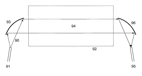
20 Figure 9 illustrates a general principle for incorporating reflective
optics into
the transmit and receive elements of an optical touch screen sensor. On the
transmit
side, light 90 emerging from transmit waveguide 91 is directed across display
area 92
by reflector 93, as beam 94, then focused into receive waveguide 95 by
reflector 96.
In general, reflectors 93 and 96 can have any concave curved shape suitable
for
25 producing a collimated or convergent beam 94. Each may for example comprise
a
portion of a circle, ellipse, parabola or hyperbola, or any curve generated by
a
polynomial equation. Each may also comprise pluralities of straight segments
that
CA 02597009 2007-08-07
WO 2006/081633 PCT/AU2006/000152
-20-
approximate a curved surface. In a preferred embodiment, reflectors 93 and 96
are
parabolic in shape. In another preferred embodiment, reflectors 93 and 96 are
elliptical in shape.
The invention will be described in terms of transmit and receive elements of
an
optical touch screen sensor with reduced temperature sensitivity. However it
will be
appreciated that the inventive principles apply more generally to any optical
system
comprising one or more waveguides with associated lenses, such as the
transmission
device shown in Figure 2, that is impaired by a change in the refractive index
of the
lens (and hence its refractive power) caused by a change in temperature.
It is a well known result of geometrical optics ("Optics", E. Hecht, 2 a ed.,
Addison-Wesley (1987), pp. 156-158) that a parabolic mirror provides perfect
collimation of light emitted from a point source placed at the focus of the
parabola. In
principle then, transmit and receive optics involving TIR off parabolic
polymer/air
interfaces can provide essentially temperature-independent operation of an
optical
touch screen sensor. Those skilled in the art will understand that off-axis
parabolic
interfaces are preferred so that the source and receive waveguides do not
obscure
collimated beam 94, as shown in Figure 9.
EXAMPLE 2
In accordance with the invention, a transmit element 100 incorporating a
parabolic reflector is shown in Figure 10. Transmit waveguide 102 guides light
101
through an angle P = 33.1 at bend 1007, along straight section 1008 and into
polymer
slab region 103 at point 104, whereupon it spreads with divergence angle 2~
and
encounters curved side 106 that is a portion of a parabola with focus at point
104 and
with directrix perpendicular to optical axis 105. The angle of incidence Bt
ranges from
63 at point 107 to 68 at point 108, and is always greater than the critical
angle (see
Table 4) so that the total internal reflection condition is satisfied. After
reflecting off
curved side 106, the light is collimated along optical axis 105. Straight
sides 109,
1000 and 1001 of polymer slab region 103 are 204 m, 687 m and 220 m long, and
curved sides 1002 and 106 are both 3493 m long. After reflection off curved
side
106, the light is collimated into parallel rays 1009 that exit transmit
element 100 at
end face 1003 to form transmitted beam 1004. End face 1003 is 709 m wide, and
the
CA 02597009 2007-08-07
WO 2006/081633 PCT/AU2006/000152
-21-
remaining straight sides 1005 and 1006 are both 110 m long. A receive element
is
the mirror image of a transmit element and will not be described in detail.
To form a transmit array, it is necessary to nest the transmit elements
closely
together. An example design for nested reflective transmit elements 100 is
illustrated
in Figure 11 a; as in Figures 1 and 5 the vertical collimating lenses have
been omitted
for clarity. It will be appreciated that this nesting design requires the
length of straight
sections 1008 to be incrementally varied. In an alternative nesting design,
the length
of straight sections 1008 can be held constant and the lengths of sides 1005
and 1006
incrementally varied. Note that sides 1005 and 1006 do not play any role in
the
operation of transmit element 100, and can be omitted as shown in Figure l lb,
such
that all transmit elements 100 in the array share a common end face 1003. This
configuration may be preferred over that shown in Figure 11 a, since there are
no gaps
between the individual element end faces through which foreign matter may
enter and
contaminate the reflective surfaces.
In Figure 10, it is important to note that the parallel rays 1009 always
encounter end face 1003 at normal incidence, where from Snell's Law the
temperature-dependence 'of the polymer refractive index has no effect (Bi = 9t
= 0).
Advantageously, this arrangement also yields a solution to the vertical
collimation
difficulties of the prior art transmit and receive lenses illustrated in
Figures 3a, 3b, 4a
and 4b. The positioning of vertical collimating lens (VCL) 33 with respect to
end face
1003 of a single parabolic reflector-based transmit element 100 is illustrated
in Figure
12a (plan view) and Figure 12b (side view). It will be appreciated that
because end
face 1003 is straight, it can be positioned at the focal plane 32 of VCL 33 so
that the
emerging beam 120, diverging in the vertical direction, can be focused equally
well
across its entire width to produce vertically collimated beam 121. This is in
contrast
to the situation with a lens shown in Figures 3a and 3b, where only a portion
of curved
end face 31 can be placed in the focal plane of VCL 33. Furthermore, because
end
face 1003 is straight, it can be readily cut with a dicing saw or a laser,
thereby
avoiding the shadowing effect shown in Figures 4a and 4b. Figures 13a (plan
view)
and 13b (side view) show that, for a parabolic reflector-based transmit
element 100,
there is no possibility of substrate 41 and buffer layer 42 blocking emerging
rays 43
en route to VCL 33.
CA 02597009 2007-08-07
WO 2006/081633 PCT/AU2006/000152
- 22 -
Referring to Figure 12a, yet another advantage of the inventive approach is
that during assembly, space 122 between end face 1103 and VCL 33 can be filled
with
adhesive to attach the VCL to the element array. This is not possible with the
prior art
lens approach because curved end face 31 relies on the polymer/air refractive
index
contrast. As will become clear below, it is preferable that the adhesive and
the
material used to form the transmit and receive elements are index matched, ie.
their
refractive indices are substantially equal.
With reference to Figure 10, it will be appreciated that curved side 106 in
Example 2 needs to be carefully designed and reproduced in the fabrication
process if
the light is to be perfectly collimated along optical axis 105. For example if
curved
side 106 is not perfectly parabolic in shape or if source point 104 is not at
the focus,
then the emerging beam will be slightly convergent or divergent.
Alternatively, if the
directrix of the parabolic reflective surface is not perpendicular to optical
axis 105,
then the emerging beam will be collimated in a direction that deviates
slightly from
the optical axis. In view of fabrication tolerances, an alternative embodiment
where
the transmitted beam is focused to a point between the transmit and receive
elements
may be desirable. If the transmit and receive elements of an optical touch
screen
sensor have identical size, the focal point should be located at the midpoint,
as
illustrated in Figure 14. Those skilled in the art will understand that in
this situation,
transmit side reflector 141 needs to be a segment of an ellipse with foci at
source point
142 and midpoint 143, and receive side reflector 144 needs to be a segment of
an
ellipse with foci at receive point 145 and midpoint 143. Compared to the
embodiment
with parabolic reflectors, a feature of an embodiment with elliptical
reflectors is that
the reflector design is dependent on the physical dimensions of the touch
screen
sensor, specifically the distance from the transmit and receive elements to
midpoint
143.
EXAMPLE 3
A transmit element 150 incorporating an elliptical reflector and designed for
a
65mm wide touch screen is shown in Figure 15. Transmit waveguide 152 guides
light
151 through an angle (3 = 33.1 at bend 1507, along straight section 1508 and
into
polymer slab region 153 at point 154, whereupon it spreads with divergence
angle 2~
and encounters curved side 156 that is a segment of an ellipse with one focus
at point
CA 02597009 2007-08-07
WO 2006/081633 PCT/AU2006/000152
- 23 -
154 and the other focus at point 1504 located a distance 32.5mm from end face
1503.
The angle of incidence B; ranges from 63 at point 157 to 68 at point 158,
and is
always greater than the critical angle (see Table 4) so that the total
internal reflection
condition is satisfied. Straight sides 159, 1500 and 1501 of polymer slab
region 153
are 204 m, 687 m and 220 m long, and curved sides 1502 and 156 are both 3493 m
long. After reflection off curved side 156, the light is focused into a beam
1509 that
exits transmit element 150 at end face 1503 and converges to point 1504 on
optical
axis 155. End face 1503 is 709 m wide, and the remaining straight sides 1505
and
1506 are both 110 m long. A receive element is the mirror image of a transmit
element and will not be described in detail. It will be appreciated that since
transmit
element 150 (with elliptical reflector) is virtually identical to transmit
element 110
(with parabolic reflector) in overall shape, the nesting designs shown in
Figures lla
and 1 lb are also applicable to transmit element 150, with the incremental
increases in
the length of straight section 1508.
In the interests of minimising temperature dependence, end face 1503 should
comprise an arc of a circle centred on point 1504; so that all rays of beam
1509
encounter end face 1503 at normal incidence. Since the radius of curvature of
end
face 1503 will generally be much larger than its width (the dimensions of the
touch
screen are much larger than the individual transmit and receive elements), end
face
1503 will deviate only slightly from straightness. Note however that if the
space
between the end face and the VCL is filled with an index matched adhesive
during
assembly, as mentioned above with regard to Figure 12a, the shape of end face
1503
becomes irrelevant for the optical performance, and it can therefore be made
advantageously straight. On the other hand, if space 122 is not filled with
adhesive, it
is still possible to design curved side 156 such that end face 1503 is
advantageously
straight while retaining the focusing of beam 1509 at point 1504. Although
curved
side 156 will then not be perfectly elliptical, it will still be a"quasi-
ellipticaP' curved
surface and within the scope of the invention.
Small adjustments to the reflector design may also be required once beam
diffraction (ignored in the geometrical ray optics approach used in the
previous
examples) is taken into account. Those skilled in the art will recognise that
diffraction
will cause an additional and unavoidable spreading of the light beams as they
traverse
CA 02597009 2007-08-07
WO 2006/081633 PCT/AU2006/000152
-24-
the display area. For the simple case of a Gaussian beam, the following two
examples
illustrate the effect of diffraction on a beam emitted by a transmit element
incorporating a parabolic reflector, as it traverses a 65mm wide touch screen.
EXAMPLE 4
In this example, the transmit element is designed to emit a 1mm wide beam
(ie. beam waist wo = 0.5mm) at wavelength 7~ = 850nm. According to basic
Gaussian
optics, the Rayleigh range ziz, defined as the distance over which the beam
radius
increases by a factor of 42, is given by ZR =7c w0z/k. In this example, zR is
920mm,
which is much greater than the width of the touch screen (65mm).
Alternatively, after
travelling a distance of 65mm, the beam width will have expanded only
slightly, from
lmrn to 1.034mm. It can be seen that in this example, beam diffraction is
negligible.
EXAMPLE 5
In this example, the transmit element is designed to emit a 0.25mm wide beam
(ie. beam waist wa = 0.125mm) at wavelength k = 850nm. It will be appreciated
that
narrower beams may be desirable for improved spatial resolution of the touch
screen
sensor. In this case, zR is only 58mm, less than the width of the touch
screen, and after
65mm the beam width will have expanded from 0.25mm to 0.364mm (a 50%
increase), so that beam diffraction is certainly not negligible.
To compensate for beam diffraction, it may be desirable to make slight
adjustments in the reflector design. For example, the optimum shape for the
reflector
may deviate slightly from a perfect parabola or ellipse. However it will be
understood
that such quasi-parabolic and quasi-elliptical curved shapes are within the
scope of the
invention.
Irrespective of the particular shape of the reflective surface, the nested
layouts
shown in Figures l la and llb have an additional advantage over the prior art
layout
shown in Figure 1, in terms of bend loss in the transmit side and receive side
waveguides located in the screen bezel. As Figure 1 shows, the prior art
layout
requires the transmit side waveguides 2 and receive side waveguides 3 to be
bent
through 90 , whereas the reflective optics layout requires them to be bent
through a
lesser angle; in the specific case of Exarnples 2 and 3 this angle is 33.1 .
If all other
factors (wavelength, waveguide dimensions and refractive index contrast) are
equal,
CA 02597009 2007-08-07
WO 2006/081633 PCT/AU2006/000152
- 25 -
then the bend loss will be advantageously lower in the reflective optics
layout,
representing an additional saving in the optical power budget.
It should be noted that the reflective optics designs of Examples 2 and 3 are
not absolutely temperature independent, since there remain two small effects
of the
temperature-dependence of the polymer refractive index. Both the divergence
angle
2~ inside polymer slab region 103 or 153 and the transmittance through end
face 1003
or 1503 depend on the polymer refractive index. The first effect is small but
difficult
to quantify since, for a given width of transmit waveguide 102 or 152, the
divergence
angle depends on the number and type of optical modes launched into polymer
slab
region 103 or 153. This effect will change the beam width by a small amount
(via the
positions of points 107, 108, 157 and 158) but will not affect the collimation
or focus
of the beam.
The second effect can be readily quantified from the well known Fresnel
equations ("Optics", E. Hecht, 2"d edn, Addison-Wesley (1987), pp. 94-104).
The
equation for transmittance of light propagating from a medium of refractive
index n;
into a medium of refractive index ni is particularly simple at normal
incidence, being
given by T = 4nlnt /(ni + nt)z, irrespective of the polarisation state of the
light. With
nair = 1, the transmittance of light propagating from polymer A into air (and
vice
versa) at normal incidence and at -10, 25 and 50 C is given in Table 5 below.
This
shows that less than 4.6% of light is lost in reflection at each of the
transmit and
receive polymer/air interfaces, and the temperature dependence, while present,
is
negligible over the chosen operating temperature range. Of course if the space
between the end face and the VCL is filled with an index matched adhesive
during
assembly, as mentioned above with regard to Figure 12a, there will be no
reflection
losses at the polymer/air interfaces.
Temperature/ C npolymer T
-10 1.5413 0.9546
25 1.5315 0.9559
50 1.5245 0.9568
Table 5
CA 02597009 2007-08-07
WO 2006/081633 PCT/AU2006/000152
-26-
It will be readily understood that both of the above-mentioned temperature-
dependent effects are also present in the prior art refractive optics approach
shown in
Figure 5. Furthermore when considering transmittance through the polymer/air
interfaces, the inventive reflective optics schemes shown in Figures 10 and 15
represent a simplification over the prior art refractive optics approach.
Unlike in the
inventive reflective optics scheme, where the angle of incidence at the end
face is
always zero (normal incidence), in the refractive optics approach the angle of
incidence 9; is variable, depending on the ray angle ~, and this introduces a
variability
into the transmittance through the interfaces (according to the Fresnel
equations).
Note that away from nornzal incidence the Fresnel equations also have a
dependence
on the polarisation state of the light, but this can be neglected in the
present case
because the polarisation state is expected to be random. The net effect is
that the
transmittance decreases monotonically with increasing ray angle ~,
representing
another source of optical loss. In the lens design of Example 1, where ~ is
limited to
14.4 , the transmittance at 25 C is never more than 1% below the normal
incidence
value, so that this effect is negligible. However this may not be so for lens
designs
with larger possible ray angles ~. The transmit side lens is particularly
vulnerable,
because (from geometry) Bi increases more rapidly than ~(eg. in the design of
Example 1, 81 = 26.7 when ~= 14.4 ), and if 6; approaches the critical angle
(-40.5 ), the transmittance through the polymer-to-air interface will rapidly
approach
zero. Finally, unlike the case with the inventive reflector-based transmit and
receive
elements, the reflection loss cannot be eliminated by filling the space
between the end
face and the VCL with an index matched adhesive.
EXAMPLE 6
This example describes the fabrication of an array of parabolic reflector-
based
transmit elements using a photo-patterning method. Following the synthetic
procedure disclosed in US Patent No. 6,818,721, a lower refractive index
polymer B
was prepared with a viscosity of 2400 cP (at 20 C) and a refractive index
(measured at
20 C on an Abbe refractometer with room light) of 1.498. A higher refractive
index
polymer A was prepared with a viscosity of 2300 cP (at 20 C) and a refractive
index
of 1.524 (at 20 C). A suitable photoinitiator was added to both polymer A and
polymer B.
CA 02597009 2007-08-07
WO 2006/081633 PCT/AU2006/000152
-27-
Polymer B was spin coated onto a silicon wafer and cured with UV light from
a mercury Iamp, to form a buffer layer 20 m thick and with a refractive index
of
1.5045 (at 25 C and 850nm). Polymer A was spin coated onto the buffer layer to
form a core layer 11 m thick, and patterned with UV light through a suitable
mask.
Unexposed polymer A material was then dissolved in isopropanol to leave
exposed
core material in the form of an array of parabolic reflector-based transmit
elements, as
shown for example in Figures 11a or 11b. Exposed polymer A material had a
refractive index of 1.5315 (at 25 C and 850nm). Finally, an upper cladding
layer was
deposited by spin coating a second layer of polymer B, patterning it with UV
light
through another suitable mask, and dissolving unexposed material with
isopropanol.
Note that it is necessary to pattern the upper cladding layer (as disclosed in
US
patent application No. 2005/0089298 Al) so that the reflective curved side 106
of
each transmit element retains the polymer/air interface required for total
internal
reflection. Figure 16 illustrates one possible manner for an upper cladding
160 to be
patterned, with a shaped hole 161 around reflective curved side 106. Figure 16
also
shows that upper cladding 160 can extend right up to end face 1003 of transmit
eleinent 100. This feature demonstrates yet another advantage of the inventive
reflective optics approach, as it eliminates the abovementioned mechanical
vulnerability problem of the prior art transmit and receive lenses. Reflective
surface
106 beneath shaped hole 161 is much less likely to be damaged during handling
and
assembly than an exposed curved end face, and once assembly is complete it
will be
protected within the screen bezel. Another benefit of having an upper cladding
160 is
that it will fill the gaps (if any) between sides 1005 and 1006, preventing
ingress of
foreign matter (such as uncured adhesive) that could contaminate reflective
curved
side 106.
EXAMPLE 7
This example describes the fabrication of an array of parabolic reflector-
based
transmit elements using a moulding method.
A layer of photoresist was spin coated onto a silicon wafer and exposed to UV
light through the same mask used to pattem the polymer A layer in the previous
example. Unexposed photoresist was then dissolved in isopropanol to produce a
CA 02597009 2007-08-07
WO 2006/081633 PCT/AU2006/000152
- 28 -
master with the desired waveguide pattem. Polydimethylsiloxane (PDMS) was cast
onto the master, cured and peeled off to form a stamp.
High refractive index polymer A and low refractive index polymer B were
prepared as in example 6. To fabricate the waveguide array, polymer B was spin
coated onto a silicon wafer and cured with UV light to form a 20 m thick
buffer
layer, then polymer A was spin coated onto the buffer layer to form an 11 m
thick
core layer. The PDMS stamp was then applied to the polymer A layer, the
polymer
cured with LTV light and the PDMS stamp peeled off. Optionally, an upper
cladding
layer can be deposited and patterned, either with LJV light as in example 6 or
by a
second PDMS stamp.
PDMS is a preferred material for producing the stamp, because it has low
surface energy (and therefore does not stick to most materials) and is
transparent to
the IJV light used to cure the polymer A material.
Although the invention has been described with reference to specific examples
it will be appreciated by those skilled in the art that the invention may be
embodied in
many other forms.