Note: Descriptions are shown in the official language in which they were submitted.
CA 02597031 2011-05-02
PHASE CHIP FREQUENCY-BINS OPTICAL CODE DIVISION MULTIPLE
ACCESS
BACKGROUND OF THE INVENTION
[0003] The present invention relates to optical
communication and, more particularly, to optical code division
multiple access (OCDMA) communication networks.
[0004] Various communications schemes have been used to
increase data throughput and to decrease data error rates as
well as to generally improve the performance of communications
channels. As an example, frequency division multiple access
("FDMA") employs multiple data streams that are assigned to
specific channels disposed at different frequencies of the
transmission band. Alternatively, time division multiple
access ("TDMA") uses multiple data streams that are assigned
to different timeslots in a single frequency of the
transmission band. However, FDMA and TDMA are quite limited
in the number of users and/or the data rates that can be
supported for a given transmission band.
[0005] In many communication architectures, code division
multiple access (CDMA) has supplanted FDMA and TDMA. CDMA is
a form of spread spectrum communications that enables multiple
data streams or channels to share a single transmission band
at the same time. The CDMA format is akin to a cocktail party
-1-
CA 02597031 2007-08-03
WO 2007/053172 PCT/US2006/005834
in which multiple pairs of people are conversing with one
another at the same time in the same room. Ordinarily, it is
very difficult for one party in a conversation to hear the
other party if many conversations occur simultaneously. For
example, if one pair of speakers is excessively loud, their
conversation will drown out the other conversations.
Moreover, when different pairs of people are speaking in the
same language, the dialogue from one conversation may bleed
into other conversations of the same language, causing
miscommunication. In general', the cumulative background noise
from all the other conversations makes it harder for one party
to hear the other party speaking. It is therefore desirable
to find a way for everyone to communicate at the same time so
that the conversation between each pair, i.e., their "signal",
is clear while the "noise" from the conversations between the
other pairs is minimized.
[0006] The CDMA multiplexing approach is well known and is
explained in detail, e.g., in the text "CDMA: Principles of
Spread Spectrum Communication," by Andrew Viterbi, published
in 1995 by Addison-Wesley. Basically, in CDMA, the bandwidth
of the data to be transmitted (user data) is much less than
the bandwidth of the transmission band. Unique "pseudonoise"
keys are assigned to each channel in a CDMA transmission band.
The pseudonoise keys are selected to mimic Gaussian noise
(e.g., "white noise") and are also chosen to be maximal length
sequences in order to reduce interference from other
users/channels. One pseudonoise key is used to modulate the
user data for a given channel. This modulation is equivalent
to assigning a different language to each pair of speakers at
a party.
[0007] During modulation, the user data is "spread" across
the bandwidth of the CDMA band. That is, all of the channels
are transmitted at the same time in the same frequency band.
This is equivalent to all of the pairs of partygoers speaking
at the same time. The introduction of noise and interference
from , other users during transmission is inevitable
-2-
CA 02597031 2007-08-03
WO 2007/053172 PCT/US2006/005834
(collectively referred to as "noise"). Due to the nature of
the pseudonoise key, the noise is greatly reduced during
demodulation relative to the user's signal because when a
receiver demodulates a selected channel, the data in that
channel is "despread" while the noise is not "despread."
Thus, the data is returned to approximately the size of its
original bandwidth, while the noise remains spread over the
much larger transmission band. The power control for each
user can also help to reduce noise from other users. Power
control is equivalent to lowering the volume of a loud pair of
partygoers.
[0008] CDMA has been used commercially in wireless
telephone ("cellular") and in other communications systems.
Such cellular systems typically operate at between 800 MHz and
2 GHz, though the individual frequency bands may only be a few
MHz wide. An attractive feature of cellular CDMA is the
absence of any hard limit to the number of users in a given
bandwidth, unlike FDMA and TDMA. The increased number of
users in the transmission band merely increases the noise to
contend with. However, as a practical matter, there is some
threshold at which the "signal-to-noise" ratio - becomes
unacceptable. This signal-to-noise threshold places real
constraints in commercial systems on the number of paying
customers and/or data rates that can be supported.
[0009] Recently, CDMA has been used in optical
communications networks. Such optical CDMA (OCDMA) networks
generally employ the same general principles as cellular CDMA.
However, unlike cellular CDMA, optical CDMA signals are
delivered over an optical network. As an example, a plurality
of subscriber stations may be interconnected by a central hub
with each subscriber station being connected to the hub by a
respective bidirectional optical fiber link. Each subscriber
station has a transmitter capable of transmitting optical
signals, and each station also has a receiver capable of
receiving transmitted signals from all of the various
transmitters in the network. The optical hub receives optical
-3-
CA 02597031 2007-08-03
WO 2007/053172 PCT/US2006/005834
signals over optical fiber links from each of the transmitters
and transmits optical signals over optical fiber links to all
of the receivers. An optical pulse is transmitted to a
selected one of a plurality of potential receiving stations by
coding the pulse in a manner such that it is detectable by the
selected receiving station but not by the other receiving
stations. Such coding may be accomplished by dividing each
pulse into a plurality of intervals known as "chips". Each
chip may have the logic value "1" , as indicated by relatively,
large radiation intensity, or may have the logic value "0", as
indicated by a relatively small radiation intensity. The
chips comprising each pulse are coded with a particular
pattern of logic "1"'s and logic "0"'s that is characteristic
to the receiving station or stations that are intended to
detect the transmission. Each receiving station is provided
with optical receiving equipment capable of regenerating an
optical pulse when it receives a pattern of chips coded in
accordance with its own unique sequence but cannot regenerate
the pulse if the pulse is coded with a different sequence or
code.
[0010] Alternatively, the optical network utilizes CDMA
that is based on optical frequency domain coding and decoding
of ultra-short optical pulses. Each of the transmitters
includes an optical source for generating the ultra-short
optical pulses. The pulses comprise Fourier components whose
phases are coherently related to one another. A "signature"
is impressed upon the optical pulses by independently phase
shifting the individual Fourier components comprising a given
pulse in accordance with a particular code whereby the Fourier
components comprising the pulse are each phase shifted a
different amount in accordance with the particular code. The
encoded pulse is then broadcast to all of or a plurality of
the receiving systems in the network. Each receiving system
is identified by a unique signature template and detects only
the pulses provided with a signature that matches the
particular receiving system's template.
-4-
CA 02597031 2012-04-11
[0011] Improvements in the performance of OCDMA systems is
nonetheless of utility. For example, OCDMA systems that are
compatible with Wavelength Division Multitplex (WDM) or Dense
WDM (DWDM) systems, more spectrally efficient and less costly
are needed.
SUMMARY OF THE INVENTION
[0011a] Certain exemplary embodiments can provide an
apparatus for receiving a plurality of mutually orthogonal,
spectrally phase encoded optical signals which simultaneously
occupy the same optical frequency domain, in which each
encoded optical signal comprises a plurality of uniformly
spaced spectral lines, all of which are modulated with data
associated with each user of a plurality of users, and the
modulated signals are encoded by imposing predetermined
relative phase shifts between spectral lines according to the
code assigned to each user, comprising: a spectral phase
decoder for decoding a selected encoded optical signal to
produce a decoded signal that occupies a finite sampling
interval while at the same time nulling the optical power of
the other encoded optical signals during the sampling time; an
optical time gate for temporally extracting the selected
optical signal and rejecting other interfering optical
signals, all of which occupy the same frequency domain; and a
demodulator and detector that is operable to extract user data
from the selected optical signal; wherein the spectral phase
decoder separates the individual spectral components of the
signal, individually shifts the phase of each of the spectral
components and coherently recombines the frequency components,
so that the decoder is operable to conjugate the phase code
- 5 -
CA 02597031 2012-04-11
used to encode the encoded optical signal; and wherein the
spectral phase decoder comprises a plurality of high-
resolution, integrated optical structures each of which
separates an individual spectral component, a plurality of
phase shifters operable to conjugate the phase code used to
encode the encoded optical signals, and a matched plurality of
integrated optical structures for coherently recombining the
spectral components.
[0011b] Certain exemplary embodiments can provide an
apparatus for receiving a desired encoded optical signal
comprising equally spaced coherent phase-locked spectral lines
in the presence of other differently and orthogonally encoded
synchronous, co-polarized optical signals which occupy the
same wavelength channel and bit period, comprising: a spectral
phase decoder comprising a means for individually phase
shifting each of the equally spaced, coherent phase-locked
spectral lines of the encoded optical signal with respect to
the other spectral lines in accordance with a predetermined
code which code is one of a set of more than two mutually
orthogonal codes, for decoding the encoded optical signal to
produce a decoded signal in which the desired encoded optical
signal is reconstituted and occupies a small part of the bit
period, and the other differently encoded signals have minimal
optical power in that part of the bit period; a synchronous
optical time gate for temporally extracting the desired coded
signal from the decoded composite signal by synchronously
selecting only the portion of the bit period in which the
desired signal resides; and a demodulator that is operable to
extract user data from the user desired coded signal; wherein
- 5a -
CA 02597031 2012-04-11
the spectral phase decoder comprises a plurality of ring
resonators each of which selects one of the spectral
components which constitutes the optical signal, and which
individually couple each of the spectral components from an
input waveguide to an output waveguide and a set of optical
phase shifters, each of which operates to shift the phase of
one of the spectral components with respect to the other
spectral components.
[0012] The apparatus can include a spectral phase decoder
for decoding the encoded optical signal to produce a decoded
signal and a time gate for temporally extracting a user signal
from the decoded signal . The apparatus may further desirably
comprise a demodulator that is operable to extract user data
from the user signal.
[0013] In accordance with this aspect of the present
invention, the spectral phase decoder comprises a phase filter
that is operable to conjugate the phase of a phase filter used
to encode the encoded optical signal.
[0014] In addition, the encoded optical signal comprises a
signal encoded using a code chosen from among a set of binary
and orthogonal codes. Most preferably, the set of binary and
orthogonal codes comprise a set of Hadamard codes.
[0015] Further in accordance with this aspect of the
present invention, the spectral phase decoder preferably
comprises a ring resonator. Most preferably, the ring
resonator includes two ports, a polarization beam splitter and
a polarization rotator arranged such that an optical signal
that enters one of the two ports in a first polarization state
exits the other port in a second polarization state.
- 5b -
CA 02597031 2012-04-11
[0016] Further in accordance with this aspect of the
present invention, the decoder may comprise a planar optical
circuit constructed from multiple ring resonators and phase
filters.
[0017] Further still, the spectral phase decoder may
desirably comprise a transparent plate, a Fourier lens and a
phase mask mirror that are arranged so that the transparent
plate spectrally spreads the encoded optical signal to provide
- 5c -
CA 02597031 2007-08-03
WO 2007/053172 PCT/US2006/005834
multipath optical signals to the Fourier lens which projects
the multipath optical signals onto the phase mask mirror, the
phase mask mirror being located at the focal plane of the
Fourier lens. Most preferably, the transparent plate
comprises a first mirror having an inner surface and an outer
surface and a second mirror having an inner surface and an
outer surface, the first and second mirrors being arranged
across an air gap such their inner surfaces face each other
and wherein the inner surface of the first mirror is
reflective and the inner surface of the second mirror is
partially reflective.
[0018] Further in accordance with this aspect of the
present invention, the optical time gate is desirably
operative to filter multi-user interference energy that falls
outside a time interval in which the user signal is located.
Most preferably, the optical time gate is selected from the
group consisting of a nonlinear optical loop mirror, a
terahertz optical asymmetric time gate and a four-wave mixing
time gate.
[0019] Further in accordance with this aspect of the
present invention, the demodulator comprises an ON/OFF keyed
demodulator.
[0020] In another aspect, the present invention is an
optical system for transporting data. The system preferably
comprises a source for generating a sequence of optical
pulses, each optical pulse comprising a plurality of spectral
lines uniformly spaced in frequency; a data modulator
associated with a subscriber and operable to modulate the
sequence of pulses using subscriber data to produce a
modulated data signals; and an orthogonal encoder associated
with the data modulator and operable to spectrally encode the
modulated data signal to produce an encoded data signal.
[0021] In accordance with this aspect of the present
invention, the system may also further desirably comprise a a
matching orthogonal decoder for spectrally decoding the
encoded data signal to produce a decoded data signal.
-6
CA 02597031 2007-08-03
WO 2007/053172 PCT/US2006/005834
[0022] In accordance with this aspect of the present
invention, the source preferably comprises a mode locked laser
wherein each of the plurality of spectral lines are
approximately equal in amplitude and are phase locked. Most
preferably, the encoder comprises an Hadamard encoder that
applies a unique spectral phase component to each of the
plurality of spectral lines.
[0023] Further in accordance with this aspect of the
present invention, the system may further comprise a plurality
of additional modulators each respectively associated with
additional subscribers and each respectively operable to
modulate the sequence of pulses using data associated with the
plurality of additional subscribers to produce a plurality of
additional modulated data signals. Further still, the system
may further desirably comprise a plurality of additional
Hadamard encoders each respectively associated with one of the
additional modulators and operable to spectrally encode a
respective one of the plurality of additional modulated data
signals to produce a plurality of additional encoded data
signals. Most preferably, each of the additional Hadamard
encoders associates a unique spectral phase code with each of
the additional subscribers.
[0024] Further in accordance with this aspect of the
present invention, the system further desirably includes a
time gate coupled to the orthogonal decoder and operable to
temporally extract a subscriber data signal from the decoded
signal.
[0025] Another aspect of the present invention is a method
comprising generating a sequence of optical pulses, each
optical pulse comprising a plurality of spectral lines;
modulating the sequence of optical pulses using subscriber
data to produce a modulated data signal; and spectrally phase
encoding the modulated data signal using a set of orthogonal
codes to produce an encoded data signal.
[0026] Further in accordance with the method, modulating
preferably comprises confining the 'modulated data signal to a
-7-
CA 02597031 2007-08-03
WO 2007/053172 PCT/US2006/005834
bandwidth associated with one of the plurality of spectral
lines associated with one of the set of orthogonal codes.
Most preferably, modulating comprises
[0027] In another aspect, the method may further desirably
comprise spectrally phase decoding the encoded data signal;
and temporally extracting a subscriber data signal from the
decoded signal using an optical time gate.
BRIEF DESCRIPTION OF THE DRAWINGS
[0028] FIG. 1 illustratively depicts a system in accordance
with an aspect of the present invention.
[0029] FIG. 2A illustratively depicts a source in
accordance with an aspect of the present invention.
[0030] FIG. 2B is a spectral plot showing the modes or
lines of a laser source in accordance with an aspect of the
present invention.
[0031] FIG. 3 illustratively depicts an encoder decoder in
accordance with an aspect of the present invention.
[0032] FIGS. 4A and 4B illustratively depict an
encoder/decoder in accordance with an aspect of the present
invention.
[0033] FIG. 5A illustratively depicts an optical time gate
in accordance with an aspect of the present invention.
[0034] FIG. 5B illustratively depicts optical time gating
for multi-user interference rejection in accordance with an
aspect of the present invention.
[0035] FIG. 5C illustratively depicts a non-linear optical
loop mirror time gate in accordance with an aspect of the
present invention.
[0036] FIG. 5D illustratively depicts a terahertz optical
asymmetric time gate in accordance with an aspect of the
present invention.
[0037] FIG. 5E illustratively depicts an optical time gate
using four-wave mixing in accordance with an aspect of the
present invention.
[0038] FIG. 6 illustratively depicts a system in accordance
with an aspect of the present invention.
-8-
I I
CA 02597031 2011-05-02
[0039] FIG. 7 illustratively depicts the transfer functions
of four Hadamard encoded signals in accordance with an aspect
of the present invention.
[0040] FIG. 8 is a diagram illustratively depicting an
overlay of an OCDMA system onto a WDM system in accordance
with an aspect of the present invention.
DETAILED DESCRIPTION
[0042] FIG. 1 illustratively depicts a system 100 in
accordance with an aspect of the present invention. The
system comprises a laser source 110 that generates a sequence
of optical pulses 115 that are fed to a data modulator 120.
The data modulator 122 also receives a data stream 122 that is
used to modulate the sequence of optical pulses 115. The
modulation data preferably comprises a digital data stream
generated by a subscriber or user station 124. In a preferred
embodiment, the data modulator 122 comprises an ON/OFF keyed
data modulator wherein a "1" symbol or bit in the digital data
stream corresponds to the presence of an optical pulse and a
"0" symbol or bit corresponds to the absence of an optical
pulse. In this way, each pulse represents a bit of
information. For example, a modulated stream 125 is shown
where the digital data stream comprises a "1010" data
sequence. As shown, each time slot with the bit "1" will
result in the presence of an optical pulse (1251 and 1253),
whereas each time slot with a "0" bit indicates the absence of
an optical pulse (1252 and 1254), which are shown as dashed
lines to indicate their absence.
[0043] The modulated data stream 125 is then fed to a
spectral phase encoder 132. As is discussed in further detail
below, the spectral phase encoder 132 uses a phase mask to
-9-
CA 02597031 2007-08-03
WO 2007/053172 PCT/US2006/005834
apply a phase code associated with a user to each optical
pulse in the data stream to produce an encoded data stream
135. The phase code operates to provide a "lock" so that only
a corresponding phase decoder with the appropriate "key" or
phase conjugate of the phase code of the spectral phase
encoder may unlock the encoded data stream. Typically, a
spectral phase encoder is associated with a particular user
and therefore allows only another user with the appropriate
key to decode or receive information from the particular user.
The information appears as noise to users that do not have the
appropriate key.
[0044] The encoded data stream 135 may then be transported
over a network 140, such as Wavelength Division Multiplex
(WDM) network for example, to a spectral phase decoder 144
that, preferably, includes a phase mask that applies the phase
conjugate of the phase code of the spectral phase encoder 132,
as discussed above. The spectral phase decoder 144 provides a
decoded data stream 149 to an optical time gate 150. As is
discussed in detail below, the optical time gate 154 operates
to reduce multiple access interference by temporally
extracting only a desired user channel from among the decoded
stream. The optical time gate 154 produces a user data stream
159, which is fed to a data demodulator 164. Where ON/OFF
keying was employed at the transmitting end, the data
demodulator 164 comprises an amplitude detector that
reproduces the digital data stream 124.
[0045] In accordance with an aspect of the present
invention, the laser source 110, data modulator 122 and
spectral phase encoder 132 may comprise a transmitting station
170 associated with a user. The spectral phase decoder 144,
optical time gate 154 and demodulator 164 may preferably
comprise a receiving station 180 associated with a user.
[0046] FIG. 2A illustratively depicts a laser source 200
that may be used to generate the pulse stream 115 in
accordance with an aspect of the present invention. The laser
source 200 preferably comprises a mode locked laser (MLL)
-10-
CA 02597031 2007-08-03
WO 2007/053172 PCT/US2006/005834
having a spectral content comprising a stable comb of closely
spaced phase-locked frequencies. The frequency or comb
spacing is determined by the pulse repetition rate of the MLL.
As shown in FIG. 2A, the source 200 may comprise a ring laser
that may be formed using a semiconductor optical amplifier
(SOA) or erbium doped fiber amplifier (EDFA). The ring laser
illustrated in FIG. 2 includes a laser cavity 210, a modulator
216, a wavelength division multiplexer (WDM) 222 and a tap
point 226 for providing an output signal, which comprises
optical pulses 115.
[0047] FIG. 2B illustratively depicts a frequency plot 250
of the output of a MLL in accordance with an aspect of the
present invention. The spacing of the longitudinal modes or
lines is equal to the pulse repetition rate of 5 GHz. As also
seen in FIG. 2B, the total spectral width of the source may be
limited to, for example, 80 GHz by placing an optical band
pass filter in the laser cavity. The top portion 252 of FIG.
2B shows multiple windows that illustratively indicate the
tunability of the source. Each line or mode 256 of the laser
comprises a frequency chip or bin. FIG. 2B illustratively 16
frequency bins or chips in accordance with an aspect of the
present invention.
[0048] In general, the electric field m(t) output of the
MLL is a set of N equi-amplitude phase-locked laser lines:
N 3(2 t+o)
m(t) = AY, e ( ~ )
i=1
where f = -193THz + (i-1)df are equally spaced frequencies. Signal
in(t) is a periodic signal comprising a train of pulses spaced 11df
seconds apart and each pulse having a width equal to 1/(Ndf)
seconds. We can also express (1) as:
m(t)=Ep(t-kT) (2)
k
-11-
CA 02597031 2011-05-02
where p(t) represents a pulse of duration T=1/df whose energy is
mostly confined in the main lobe of width 11(Ndf). With' regard to
FIG. 2A, N=16 and dfis equal to 5 GHz.
[0049] Turning now to FIG. 3, there is depicted a spectral
phase encoder 300 in accordance with an aspect of the present
invention. The encoder 300 includes a transparent plate 310,
a Fourier lens 314 and a phase mask mirror 318. The plate 310
comprises a first element 320 that includes an inner surface
322 and an outer surface 326. The first element 320 is spaced
from a second element 330 that also has an inner surface 332
and an outer surface 336. The inner surface 322 of the first
element provided with a coating that is substantially 100%
reflective. The inner surface 332 of the second element is
provided a partially reflective coating. The first and second
elements 320, 330 may be separated by a glass substrate 340,
as shown, or by an air gap. The arrangement of the
transparent plate and Fourier lens comprise an optical
demultiplexer and may comprise structure or components as
described in U.S. Patent No. 6,608,721.
[0050] As shown, the first element 320 and glass substrate
340 are arranged such that an opening 342 is provided at one
end of the plate 310. The opening 342 provides an entry point
for a beam of light to enter the cavity so that a portion of
the light beam is partially reflected by the surface 332 to
surface 322, thereby establishing a cavity where the input
light beam is split into multiple beams that are each
projected onto the Fourier lens 314. The Fourier lens 314
then projects each mode or line of each beam to a particular
location in space based on the wavelength or frequency of each
mode. In particular, the phase mask mirror 318 is positioned
at the focal plane of the Fourier lens 314 such that each mode
or line is projected to a particular location on the phase
mask mirror to cause a predetermined phase shift. In this
way, the phase of each line or mode of the laser source (each
-12-
CA 02597031 2007-08-03
WO 2007/053172 PCT/US2006/005834
such line or mode comprising a frequency bin or chip) is
adjusted by a predetermined amount by the phase mask mirror.
The phase mask mirror 318 then reflects the phase adjusted
signals back through the Fourier lens 314 to the plate 310
where the phase adjusted signals exit through opening 342 as a
collimated phase adjusted beam of light.
[0051] As shown in FIG. 3, each section of the phase mask
318 is recessed at 0 or A/4 with respect to the focal plane of
the Fourier lens 314 thereby representing a 0 or it phase
shift, respectively. The phase mask of FIG. 3 includes five
sections which comprise a "10110" phase mask, wherein a "1"
represents a phase shift of it and a "0" represents a phase
shift of 0. As is discussed in further detail below, each
user is assigned a unique phase mask that includes a section
for each frequency bin or chip in the system. The unique
phase mask corresponds to a unique code or lock that is
associated with a particular user such that a receiving unit
needs the appropriate code or key to decipher a message from
the particular user. In addition, the encoder 300 may also be
used at the receive end as a decoder.
[0052] The encoder/decoder of FIG. 3 is typically large
since it uses bulk optics. The size of such encoders/decoders
typically make them susceptible to thermally induced drifts.
Furthermore, the large size and complex alignment requirements
may make it unlikely that the coder/decoder of FIG. 3 will be
economically viable. As discussed above, spectral phase
encoding consists of demultiplexing the various spectral
components of a signal, shifting the phase of a portion of the
spectrum based on the code and recombining the shifted
components to produce the coded signal. The recombined signal
no longer comprises a short optical pulse, but instead, the
energy in the pulse is spread across the bit period in a
pattern determined by the code. In accordance with an aspect
of the present invention, we use a coder/encoder in form of an
integrated photonic circuit, which uses ring resonators as
-13-
CA 02597031 2007-08-03
WO 2007/053172 PCT/US2006/005834
wavelength selective subcomponents. FIG. 4A illustratively
depicts a functional diagram of such a coder 360.
[0053] As shown in FIG. 4A, light enters from the left on
the input guide 362. At a first ring resonator structure 365,
subwavelength Al is coupled off the guide 362 and onto the
connecting guide (vertical line 367). At the bottom of
vertical line 367, Al is coupled onto the output guide 368 with
another wavelength selective ring resonator. Each of the
frequency components is coupled in the same way at the
appropriate point. If all the connecting guides have the same
optical length, and if the input and output guide have the
same propagation constant, then all frequency components will
see the same optical path length when they reach the end of
the output guide. In this case, all would recombine with the
same phase that they had at entry (i.e., this is equivalent to
a code with all 0's or all l's). To create a phase shift that
defines a code, we use heaters on the connecting waveguides,
shown here as blocks 372. The electrical connections to the
heaters are not shown to avoid unnecessarily complicating the
diagram. If the connecting waveguides are far enough apart,
then they are sufficiently thermally isolated that the phase
shifts can be applied independently. With thermal monitoring
and feedback, independent phase shifts can be applied to each
frequency even when the guides have some affect on each other.
[0054] A decoder typically has the same structure as an
encoder, except that it may need to be polarization
insensitive, since the signals may have their polarization
altered in transmission through the fiber. The coder can have
polarization dependence, since the initial mode-locked laser
pulse is polarized. An example of a polarization independent
coder is shown in FIG. 4B.
[0055] Note that each frequency passes through the same
number of elements (two ring resonators for its frequency, and
N-1 ring resonators that it passes through without being
dropped/added) and the same optical path length, except for
the phase shift that is applied thermally. Thus, each should
-14-
CA 02597031 2007-08-03
WO 2007/053172 PCT/US2006/005834
experience the same loss. Consequently, there is no skewing
of the amplitudes and the decoded pulse shape will be the same
as the input to the coder. In addition, because the base path
lengths are the same (except for some trimming to adjust for
fabrication error) creating the correct phase relationships
will typically be straightforward.
[0056] For polarization insensitivity we use the same
structure at the core, but separate input polarizations, and
have them pass through the coder/decoder 380 as shown in FIG.
4B.
[0057] As shown in FIG. 4B, light enters and passes through
an optical circulator 383. The light is split into two
polarizations using a polarization beamsplitter (PBS) 385 and
one polarization follows the upper path 387 while the
orthogonal polarization follows the lower path 389. On the
lower path a polarization rotator 391 converts the
polarizations from one mode to another orthogonal mode, e.g.,
P1 into P2 (or vice versa). The light in the upper path enters
the coder structure 393 in polarization mode 1 at the point
previously called the input 362, and the light in the lower
path enters the coder also in polarization mode 1, but at the
point previously called the output 368, traveling in the
opposite direction. The light from the upper path exits the
coder, passes through the polarization rotator and is
converted to polarization mode 2, which then passes through
the PBS 385 and is sent back to the circulator 383 from which
it exits along the path shown as a vertical line 395. The
light from the lower path, now in polarization mode 1, goes
through the coder in the opposite direction, but experiences
precisely the same phase shifts and optical path lengths as
the light from the upper path. It exits the coder and is
recombined in the PBS 385, and exits the circulator 383 in the
same way as the light from the other path. Thus, this
comprises a polarization independent component. The
structures that are shown in block 385 can either be realized
in fiber or can be built onto an optical waveguide. Without
-15-
CA 02597031 2007-08-03
WO 2007/053172 PCT/US2006/005834
this polarization independent construction, it would be
necessary to have a polarization sensor and a dynamic
polarization rotator before the decoder. Note that in this
design, path lengths are the same and the path is the same for
both polarizations. The difference is that the two
polarizations traverse the path in opposite directions.
[0058] Returning to FIG. 1, the encoded signal 135 is then
transmitted over a network 140 to a decoder 144. In a
preferred embodiment, the network 140 comprises a WDM network.
In such an implementation, the OCDMA network comprises an
overlay architecture that is compatible with existing WDM
network technologies as is discussed in further detail below.
[0059] As discussed above, the encoded signal 135 is
decoded by a spectral phase decoder 144. A spectral phase
decoder 144 will typically comprise the arrangement shown in
FIGS. 3 and 4, except that, in general, the decoder will
applythe phase conjugate of the phase mask applied by the
encoder. Note, however, and as is discussed in further detail
below, that where the phase mask uses a binary coding scheme,
the code at the decoder is its own complement and consequently
the coder and decoder are identical.
[0060] Turning now to FIG. 5A, there is shown an optical
time gate 400 in accordance with an aspect of the invention.
The decoded signal 149 has the sequence or train of optical
pulses restored to their original position within the bit
period and shape. However, the desired user signal needs to
be separated or extracted from other user signals included in
the decoded signal 149. In accordance with an aspect of the
present invention, an optical time gate, such as optical time
gate 400, may be used to reduce multiple access interference
(MAI). The optical time gate 400 filters out MAI by
temporally extracting only desired user signal or channel from
among any other signals comprising the decoded signal 149. As
shown in FIG. 5A, the optical time gate 400 includes an input
port 406 and a switch 408 that is controlled by a control
-16-
CA 02597031 2007-08-03
WO 2007/053172 PCT/US2006/005834
signal 410. The control signal 410 may be an electrical or
optical signal.
[0061] The concept behind the application of optical time
gating to extract the decoded OCDMA signal is illustrated in
FIG. 5B. Through the proper selection of an appropriate code
set for a synchronous coherent OCDMA system, a system may be
designed such that the multi-user interference energy falls
outside a time interval where the properly decoded signal
pulse resides. Therefore, by optically gating the composite
signal in order to provide low loss within the desired time
window while at the same time providing for high extinction
outside that window, one can extract only the properly decoded
signal bit stream.
[0062] For the purposes of application to a coherent
optical CDMA system, some of the more important performance
metrics for. optical gating technologies include:
-Gate width (typically on the order of 10 ps or less)
-Gate repetition rate (comparable to data rate, typically
>1 GHz or higher)
-Gate extinction rate (depends upon number of users but
typically 10-20 dB)
-Data pulse energy levels and dynamic range
-Gating control/clock pulse energy levels and dynamic
range
[0063] As a result of these performance requirements,
relatively high-speed optical processing techniques must
typically be employed, such as those used for all-optical
demultiplexing. Although there are a wide variety of options,
some of the technologies that have been demonstrated
specifically for coherent OCDMA systems include:
-Nonlinear interferometers
-Four-wave mixing (FWM) techniques
-17-
CA 02597031 2007-08-03
WO 2007/053172 PCT/US2006/005834
Both optical fiber-based and semiconductor optical amplifier
(SOA)-based approaches to these techniques are possible.
[0064] Fiber-based nonlinear interferometers for optical
time gating
[0065] By using an optical clock pulse in order to alter
the effective phase shift through one arm of an
interferometer, one can construct an all-optical gate. The
phase changed can be accomplished through a distributed
medium, such as nonlinear propagation through a length of
optical fiber, or it can be a concentrated nonlinearity, such
as can be accomplished with a semiconductor optical amplifier
(SOA). Since interferometers generally require stabilization
for proper operation, a common approach for fiber-based
nonlinear interferometers, which generally require long
lengths of fiber and therefore path lengths can drift with
environmental conditions, is the nonlinear optical loop mirror
(NOLM). With reference to FIG. 5C, the NOLM is built in a
Sagnac interferometer configuration, which by its construction
is self-stabilizing.
[0066] The operation of the NOLM can be described as
follows, assuming for simplicity that the input signal is a
single optical pulse. The incoming signal, input at Port A, is
split into two counterpropagating pulse replicas at a 50:50
fiber coupler. When the clock pulse, which can be injected at
Port C, is not present, the low amplitude data pulses simply
counterpropagate around the loop and recombine at the coupler.
The interference condition is such that signals interfere
destructively at the output port B, but interfere
constructively at the original input port A, thereby
reflecting the data pulse. On the other hand, by injecting a
large amplitude clock signal that is of a close but
distinguishable wavelength relative to the data pulse
wavelength, it is possible to overlap the clock pulse with the
clockwise propagating data pulse and introduce a nonlinear
phase shift of it. In this case, the interference condition is
-18-
CA 02597031 2007-08-03
WO 2007/053172 PCT/US2006/005834
altered such that the data pulse now exits at port B. An
optical bandpass filter at Port B suppresses the remaining
clock signal, leaving only the desired gated data pulse. The
width of the time gating window for the NOLM is defined by the
overlap between the clock and co-propagating data pulse. The
first NOLMs that were constructed required very long
dispersion-shifted fibers (>1 km) to obtain the required
nonlinear phase shift; however, recent developments in highly
nonlinear fibers have allowed for a reduction in fiber length
to approximately 100 meters or less. In conjunction with
optical thresholding, the NOLM optical time gate has been
successfully applied to an implementation of phase-coded OCDMA
system.
[0067] SOA-based nonlinear interferometers for optical time
gating
[0068] The nonlinear phase change required in the NOLM can
be accomplished by other means, such the use of as a
semiconductor optical amplifier (SOA), allowing for the
potential of device integration. An interferometric
architecture similar to the NOLM can be used, as shown in FIG.
5D. When the SOA is offset from the center of loop by lax, the
device is referred to as the terahertz optical asymmetric
demultiplexer or TOAD.
[0069] Similar to the NOLM, when the clock pulse is not
present, incoming data pulses reflect from the TOAD. By
injecting a clock pulse, which is typically chosen to be on
the order of 10 dB larger in amplitude than the data pulse
intensity, gating can occur. The clock pulse saturates the
SOA, thereby changing its effective index. The clock pulse,
which travels only in the clockwise direction, is injected
following the clockwise propagating data pulse to give the
clockwise data pulse the opportunity to propagate through the
SOA before the clock pulse saturates the SOA index. Since the
SOA slowly recovers on the time scale of hundreds of
picoseconds, counterpropagating data pulses that arrive
-19-
CA 02597031 2007-08-03
WO 2007/053172 PCT/US2006/005834
immediately after the clock pulse event has occurred see the
SOA in approximately the same relative state and do not
experience a differential phase shift. The temporal duration
of the gating window is set by the offset of the SOA, Lx, from
the center of the loop. As the offset is reduced, the gating
window width decreases until the actual length of the SOA
needs to be taken into account. The nominal gate width is
related to the offset by
Atgate = 2AX/Cfiber
where Cfiber is the speed of light in fiber. Gating windows as
short as 1.6 picoseconds have been demonstrated experimentally
using a TOAD. The TOAD optical time gate has been successfully
applied to an implementation of SPC-OCDMA.
[0070] Four wave mixing (FWM) optical time gating
[0071] Another approach to optical time gating is through
the use of four wave mixing (FWM), e.g., see FIG. 5E. FWM is a
third-order nonlinearity, similar to intermodulation
distortion in the electrical domain. In FWM, the nonlinear
beating between the data signal and a control signal at a
different wavelength generates new optical tones as sidebands.
FWM-based gating can be accomplished in optical fiber or in
waveguide devices such as semiconductor optical amplifiers
(SOAs).
[0072] In SOAs, FWM occurs through carrier density
modulation. Two co-polarized optical signals are coupled into
the SOA. One is the control signal at frequency fe and
typically has a much higher intensity than the other input
signal (data) to be wavelength converted, which is at
frequency fd. The two co-propagating signals mix and, through
carrier density modulation, form an index grating off which
signals can be scattered. The scattering of the control
signal from this grating generates two waves, one at the data
-20-
CA 02597031 2011-05-02
frequency and one at a new frequency, fa,Nered = 2f, - fd. This is the
useful wavelength- converted signal. In addition, data signal
scattering also generates two much weaker waves, one at the
control frequency and one at a new frequency, fsar~rr,re = 2 fe - fd. This
is called the satellite wave and is generally not used.
[0073] By injecting a short optical control pulse along
with the incoming OCDMA signal into the SOA as shown in FIG.
5E, it is possible to create an optical time gate by filtering
out the resulting wavelength converted signal. The clock pulse
is temporally aligned to the correct position relative to the
desired OCDMA pulse, and an optical bandpass filter is placed
at the output of the SOA in order to extract the FWM signal
only. The FWM optical time gate has been successfully applied
to an implementation of TPC-OCDMA.
[0074] Returning to FIG. 1, the signal 159 from the optical
time gate, such as time gate 400, is then supplied to data
detector and demodulator block 164. Where the data modulation
was done using ON/OFF keying the data and demodulator block
may comprise an amplitude demodulator that reproduces the
subscriber data. In this regard, any known amplitude
modulator may be employed to perform this task.
[0075] Turning now to FIG. 6, there is shown an example of
a multi-user OCDMA system 500 in accordance with an aspect of
the present-invention. In addition to illustrating an overall
system architecture 510, FIG. 6 also includes a diagram 516
that depicts signal flows through the system in the time and
frequency domain. In particular, the spectrum and temporal
intensity of the optical source 520 is identified by arrow
5161; after ON/OFF data modulation by arrow 5162; after phase
encoding by arrow 5163; after mixing all users by arrow 5164;
after the decoder of the first user by arrow 5165; and after
time gating and optical-to-electrical (O/E) conversion by
arrow 5166.
[0076] The optical source 520 comprises a phase-locked
multi-wavelength laser with an output spectrum as shown in
-21-
CA 02597031 2011-05-02
FIG. 2B. In accordance with this aspect of the present
invention, sixteen lines in the output spectrum (see lines 2561
through 25616 in FIG. 2B) comprising sixteen frequency bins or
chips are used to communicate user data across the system 500.
As FIG. 6 shows via arrow 5161r a train or sequence of pulses
522 are generated by the source 520. The spectral content of
each pulse is depicted in the frequency plots 524. The
electric field m(t) for the output of the source may be
expressed as shown above in equations (1) and (2). Therefore,
in accordance with the sample network of FIG. 6, N=16 and dj~-16
GHz as those variables are used in equations (1) and (2). In
the practical sense, the total spectral width of the source's
output is limited to a total spectral width of 80 GHz, which
results in each pulse having a width of approximately 12.5
picoseconds (ps).
[0077] The output signal 522 is provided to each of the
data modulators 530, through 530N. In keeping with the present
example N=16. As such, the system preferably includes 16
users or subscribers that each provides data 5321 through 532N
that is used to respectively modulate the pulse train or
output signal 522. In the system of FIG. 6, the data
modulators 530 operate to provide ON/OFF keying resulting in
time-domain signal 534. In the time domain signal 534, the
pulses with a solid outline indicate a "1" symbol or bit and
the pulses with dotted outline represent a "0" symbol or bit,
as previously discussed. The spectral content of such a
signal is shown in frequency plot 536.
[0078] Each of the modulated optical pulse signals are then
fed to respective spectral phase encoders 5401 through 540N as
shown. Encoding consists of separating each of these
frequency bins (2561, 2562, etc.), shifting its phase, in this
case by 0 or It, as prescribed by the choice of code, and
recombining the frequency bins to produce the coded signal.
When the relative phases of the frequencies are shifted, the
set of frequencies is unaltered, but their recombination
-22-
CA 02597031 2007-08-03
WO 2007/053172 PCT/US2006/005834
results in a different temporal pattern, e.g., a pulse shifted
to a different part of the bit period, multiple pulses within
the bit period, or noise-like distribution of optical power.
Each OCDMA code is desirably defined by a unique choice of
phase shifts. Preferably, a set of codes is chosen that makes
efficient use of the spectrum within the window, and that can
also be separated from each other with acceptable error rates,
even when a maximum number of codes occupy the window.
[0079] For the system 500 we chose the set of Hadamard
codes, which are orthogonal and binary. This choice is
desirable it that is can achieve relatively high spectral
efficiency with minimal multi-user interference (MUI). In
accordance with an aspect of the present invention, this
coding schemes offers orthogonally in the sense that MUI is
zero at the time that the decoded signal is maximum. The
number of orthogonal codes is equal to the number frequency
bins; hence, relatively high spectral efficiency is possible.
Binary Hadamard codes are converted to phase codes by
assigning to +1's and -1's phase shifts of 0 and 7t, respectively.
To encode data, which contains a spread of frequencies, as
opposed to the unmodulated pulse stream, which contains only
the initial comb of frequencies produced by the MLL, it is
preferable to define frequency bins around the center
frequencies. Encoding data then consists of applying the
phase shift associated with a frequency to the entire bin.
The output of the phase encoder is then a signal obtained by
summing the phase-shifted frequency components of the
modulated signal, or equivalently, by convolving the modulated
optical signal at the input of the phase encoder with the
inverse Fourier transform of the phase code.
[0080] Applying any of these orthogonal codes (except for
the case of Code 1, which leaves all phases unchanged) results
in a temporal pattern which has zero optical power at the
instant in time where the initial pulse would have had its
maximum power. Although this choice of orthogonal codes
-23-
CA 02597031 2007-08-03
WO 2007/053172 PCT/US2006/005834
implies synchronicity as a system requirement, since
desynchronization will move unwanted optical power into the
desired signal's time slot, careful code selection allows some
relaxation of this requirement. For example, simulations
indicate that for four simultaneous users transmitting at 2.5
Gb/s and using a suitably chosen set of four codes among the
set 16 Hadamard codes of length 16, up to 15 ps of relative
delay can be tolerated with a power penalty within 1 dB at a
BER of 10-9. Better resiliency to asynchronism may be achieved
by using multiphase codes.
[0081] Phase coding of the individual spectral components
requires a demultiplexer with sufficient resolution and path-
length stability and a means of shifting phases independently
for each frequency. In accordance with an aspect of the
present invention the coder/decoder of FIG. 3 was used to
encode the signal using a set of Hadamard codes. As
previously discussed, the coder/decoder of FIG. 3 is based on
a modified reflective geometry optical demultiplexer and which
is described in the 1721 patent. FIG. 6 shows the spectral
response of the coder for codes 9, 12, 14, and 15, from the
Hadamard-16 code set, as measured using a broadband source;
the phase shifts are shown below the spectrum. The encoder
used has a free spectral range of 100 GHz and a resolution of
-1 GHz. As FIG. 3 shows, all MLL lines are spectrally spread
by the multipath glass substrate and imaged on the focal
plane, from which they are reflected back to an output fiber.
A phase mask at the focal plane shifts each line by an amount
determined by a particular OCDMA code. The phase mask contains
16 sections representing the 16 frequency bins, each section
recessed at 0 or X/4 with respect to the focal plane
representing 0 or it phase shift, respectively. Because of the
finite spot size of the image at the focal plane, the
effective bandwidth of the frequency bin is less than the bin
spacing.
-24-
CA 02597031 2007-08-03
WO 2007/053172 PCT/US2006/005834
[0082] In its idealized form, the encoder for user i acts
as a phase-mask filter with frequency response E(`(f):
E ( (f) c(!) Recto (f - f = )
j-1 f (3)
where cq) are complex symbols indicating the j-th (1<j<N) element of
the i-th code c() and the function Rectw(f) denotes the
rectangle function of unitary amplitude and width W defined as:
Reaw(f)= 11,ifI <W/2
0, otherwise (4)
Although in principle the elements of code c(`) can take any
complex value, the phase mask currently employed allows only
for unitary amplitude and binary phase values:
ja(i)
cat) = e J , with ail) E {0,;r} = cal) E {- 1, 1} (5)
Ideally, all the spectral components of the unencoded signal
would emerge from the encoder unchanged in amplitude but, in
some cases, flipped in phase. Due to the finite diffraction-
limited spot size of the imaging optics, a spectral component
situated at a phase transition boundary (or bin edge) will
overlap two values of cq)and effectively be cancelled.
[0083] The bin edges are shown as sharp boundaries in FIG.
7. The sharp dips in FIG. 7 corresponds to boundaries between
two bins with different phase shifts where destructive
interference occurs between the two oppositely phased halves
of the light spot. The resolution of the OSA (0.01 nm, or
approximately 1.245 GHz) reduces the apparent depth of these
-25-
CA 02597031 2007-08-03
WO 2007/053172 PCT/US2006/005834
dips. Where adjacent bins have the same phase, there is no
dip in the spectrum. This coder provides stable phase shifts;
while thermal dimensional changes can shift optical paths, the
relative path lengths for adjacent frequencies is unaltered.
[0084 This passive structure imposes no intrinsic power
loss; although the current implementation has 5 dB loss, this
can be reduced. As the number of bins increases there is no
intrinsic increase in loss, and hence this approach to coding
has better scalability than time domain approaches such as
Fast Frequency Hopping. The filter bandwidth narrowing
affects the ability of the coder to process data, as opposed
to an unmodulated pulse stream. When the coded signal carries
data the entire bandwidth of the modulated signal of a given
MLL line must fit within the frequency bin as physically
defined by the geometry of the phase encoder's focal plane.
Simple on-off keying at rates equal to the bin spacing (5 GHz)
spreads the frequency into the unusable region between bins;
thus we need a modulation scheme with adequate bandwidth
compression to ensure proper transmission. This is because
the use of binary codes causes destructive interference at the
[O,n] boundaries. On-off key modulation at 2.5 Gb/s, using two
pulses per bit from a MLL running at a pulse-repetition rate
of 5 GHz satisfies this physical restriction. Alternative
approaches using duo-binary or single sideband modulation for
bandwidth compression will also ensure that the spectral
constituents of the data-modulated signal stay within their
respective frequency bins even at a data rate of 5 Gb/s. In
addition, other modulation formats such as multi-pulse ON/OFF
keyed modulation (e.g., two or more optical pulses per data
hit) and multi-phase/multi-amplitude modulation (e.g., DPSK,
QPSK, QAM and higher-order amplitude/phase modulation) may be
used. When multiphase codes that do not exhibit 0-7t phase
transitions are used, the amplitude dips at the bin edges are
reduced.
-26-
CA 02597031 2007-08-03
WO 2007/053172 PCT/US2006/005834
[0085] Due to the bin edge effects in the phase mask, the
OOK (ON/OFF Keying) modulation rate is preferably chosen so
that the spectrum broadening of each of the N spectral lines
is confined to df/2 Hz. OOK modulation at a rate of Rb=df/2
bits/sec that uses multiple pulses from the MLL to represent a
single bit satisfies this physical restriction. As an
alternative, using duobinary encoding and then modulating at
the full rate Rb=df bits/sec ensures that the spectral
constituents of the data-modulated signal stay within their
respective df--wide frequency bins. In principle, if no
amplitude bin-edge effect were present, full rate modulation
would be possible even without line coding. Therefore, after
modulation the temporal expression of the signal pertaining to
the i-th user can be written as follows:
O) (t) E akl> p(t -- kT ) (6)
k
where 4 E {0,1} is the sequence of information bits of user i.
After phase encoding, we obtain:
S (Z) (t) = b(Z) (t) * e(l) (t) _ Ea(')q(t) (t - kT)
k (7)
where e((t)=FT-1{E(i)(f)I is the impulse response of the spectral
phase encoder E(`)(f) as defined above; FT1 is the inverse Fourier
Transform (]FT) operator; q'`0(t) p(t)*e(`)(t) represents the pulse shape
of user i after encoding. If we neglect the effects of the
pulse output by the MLL, the shape of the pulse is governed by
the phase mask.
[0086] As shown in FIG. 6, the effect of phase encoding is
to spread in time, as shown by plot 545, the MLL narrow pulses
of width 1/(NA) seconds across the whole pulse interval.
-27-
CA 02597031 2007-08-03
WO 2007/053172 PCT/US2006/005834
Therefore, the proposed phase encoded OCDMA can be considered
as. the dual version of conventional direct sequence CDMA (DS-
CDMA) based on frequency spreading.
[0087] The encoded N user signals are combined 550 prior to
transmission over the fiber link and through network 556. The
network 556 preferably comprises a Wavelength Division
Multiplex (WDM) network that allows the signals of the system
500 to be transported transparently to the other signals that
are normally carried by the WDM network. In that regard, the
system 500 advantageously uses a relatively small and tunable
window, which is compatible with WDM systems that are
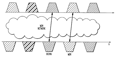
currently deployed. FIG. 8 illustratively depicts how an
OCDMA system in accordance with the various aspects of the
present invention may be overlaid on such a network. Note,
however, any other optical network may be used in accordance
with this aspect of the present invention if a tunable source
is used. As FIG. 8 shows, the OCDMA signals may be
multiplexed into the WDM channel.
[0088] Returning to FIG. 6, after the encoded signals
traverse the network 556, they are split 570 and provided to a
plurality of matching decoders 570. In particular, decoding
may be accomplished by using a matched, complementary code;
for the binary codes used here, the code is its own complement
and consequently the coder and decoder are identical. The
decoded signal has the pulses restored to their original
position within the bit period and restores the original pulse
shape. Decoding using an incorrect decoder results in a
temporal pattern that again has zero optical power at the
center of the bit period and the majority of the energy for
that pulse is pushed outside the time interval where the
desired pulse lies.
[0089] Assuming ideal fiber propagation, discrimination of
the i-th user is performed using a decoding filter d")(t) at the
receiver matched to the encoder filter only (single user
matched filtering). In general, this may be achieved by
-28-
CA 02597031 2007-08-03
WO 2007/053172 PCT/US2006/005834
employing at the receiver side a decoder equal to the
conjugate of the phase mask used at the transmitter side:
Y (Z) (t) = x(t) * d (Z) (t) (9)
where P (t) is the impulse response of the matched filter
d(l)(t)=e*(Z)(-t)<=:> D(l)(f)=E*(t)(f) (10)
The output of the filter matched to the desired user i can be
expressed as follows (assuming 240=0) :
y(Z)(t)=b(z)(t)*ACi(t)+ M b (j) *CCji(t-~-(j))
(11)
j=1, jai
where we have defined as ACi (t) = e(') (t) * e*(i) (-t) and as
CSC ji (t) = e (t) e (-t) the autocorrelations (ACs) and the
cross correlations (CCs) of the impulse responses of the phase
masks, respectively. The ACs and CCs are a function of the IFT
of the sequences used as phase masks. As opposed to the case
of conventional CDMA based on DS spreading, correlations are
between the IFT of codes, not between the codes themselves.
The effect of a matched phase decoder is to restore the
original narrow pulses of width 1/(NOf) seconds that were
originally spread in time by the phase encoder (see plot 576).
The effect of a mismatched phase decoder is to turn
interfering signals into a noise-like signal. When orthogonal
codes are employed, as opposed to conventional OCDMA, true
orthogonality is achieved here and no Multiple Access
Interference (MAI) is present at the ideal sampling time.
-29-
CA 02597031 2012-04-11
[0090] As discussed above, the signal from the phase
decoder 570 is then be further processed by an optical time
gate 580 and demodulator 590 to reproduce the user or
subscriber data signal. As also seen in FIG. 6, a
synchronization block 494 is coupled to each of the optical
time gates 580. The synchronization block 594 supplies a
control or clock signal that closes the time gate at the
proper time interval as is discussed above in relation to FIG.
5.
[0091] Although the invention herein has been described
with reference to particular embodiments, it is to be
understood that these embodiments are merely illustrative of
the principles and applications of the present invention. It
is therefore to be understood that numerous modifications may
be made to the illustrative embodiments and that other
arrangements may be devised.
-30-