Note: Descriptions are shown in the official language in which they were submitted.
CA 02598056 2007-08-15
DESCRIPTION
Method for Processing Material by Laser Ablation and Material Processed by
Processing Method Thereof
TECFINICAL FIELD
The present invention relates to a method for processing a material by laser
ablation and to the material processed by the processing method, in particular
to a
method for processing a material which has a region that receives minor
adverse affects
by the variation of pulse widths, using a laser beam having a pulse width
within the
region.
BACKGROUND ART
Conventionally it has been widely performed to direct a strong, locally-
concentrated laser beam (light) onto a material to cause physical or chemical
changes in
the irradiated part of the material, for processing such as welding, fusion
recrystallization, drilling, and cutting. When performing the above, a pulsed
oscillation,
in comparison with a continuous wave oscillation, is characterized in that
controlling
laser output light is possible by varying oscillation frequency, irradiating
an object based
on laser energy with considerable accuracy is possible because emission energy
per pulse
can be enhanced, and processing capability is high even when the average
output is
relatively low because a peak value of emission energy is high, and the like.
Therefore,
a pulsed laser beam is widely used for processing metals, living bodies,
resins and the
like.
Furthermore, the use of a laser beam having a small pulse width (short
duration),
especially a pulse width on the femtosecond (10"15) time scale has been
proposed for the
purposes of locally concentrating laser ablation, decreasing adverse affects
on peripheral
areas adjacent to the processed spot, and inducing breakdown in a desired
pattern in the
interior or exterior of the material (International Publication No. 95/27587
pamphlet
-1-
CA 02598056 2007-08-15
(see Patent Document 1)).
Patent Document 1: International Publication No. 95/27587 pamphlet
DISCLOSURE OF THE INVENTION
PROBLEMS TO BE SOLVED BY THE INVENTION
However, when using a laser beam having a small laser pulse width (short pulse
duration), especially a femtosecond laser beam, it is considered that the
chart showing
the relationship between fluence breakdown threshold, i.e., ablation
threshold, and laser
pulse width, defines a curve and exhibits a rapid and distinct change in slope
of the curve,
as shown in Patent Document 1. This means that the ablation threshold largely
varies
with the varying laser pulse width. However it is difficult to precisely
control the pulse
width of the laser used for processing materials since the laser has a large
output as well
as high-density energy. Conventionally, therefore, when processing materials
by a laser
beam with a small laser pulse width, especially by a femtosecond laser beam,
various
measures were thought to be necessary in order to ensure high precision. An
object of
the present invention is to provide a method for processing a material by
laser ablation in
which controlling laser pulse width is easy and processing with high precision
is
efficiently performed, and a material of high precision that has been
processed by the
processing method.
MEANS FOR SOLVING THE PROBLEMS
The inventors have worked diligently in order to find better processing
techniques by directing pulsed laser to a material while varying different
kinds of
parameters, such as the laser light wavelength, laser pulse width, distance
between a
work piece material and the focal point of the laser beam, and the like.
Consequently,
the inventors have found that there is a highly preferable relationship, for a
specific
material, for processing between the laser pulse width and breakdown threshold
of the
material through the ablation in a region of specific laser pulse widths, and
completed
the present invention.
The invention is a method for processing a material by laser ablation using a
-2-
CA 02598056 2007-08-15
pulsed laser beam, characterized in that the material having a region of which
a double
logarithmic chart shows a linearly-shaped line with a gradient of not more
than 0.5,
when a relationship between a laser pulse width and an ablation threshold is
represented
in the double logarithmic chart with a laser pulse width in picosecond plotted
along the
horizontal axis and an ablation threshold in J/cm2 plotted along the vertical
axis, is
processed by the pulsed laser beam having a laser pulse width within the
region.
The laser pulse width is easily controlled according to the invention, since
processing utilizing laser ablation is performed within the range for which
the
logarithmic chart representing the relationship of the ablation (ablation:
ejection of
neutral atoms and positively/negatively-charged ions of the material)
threshold and laser
pulse width exhibits a linearly-shaped line.
The ablation threshold largely varies with the varying laser pulse width even
in
F ._7=w,
the regiob where the line is linearly-shaped if the gradient of the chart (the
angle with the
horizontal axis) is large. According to the present invention, however, since
the
gradient of the chart is not more than 0.5, the adverse affects on the
ablation breakdown
caused by the variation of laser pulse width can be minimized and highly
accurate
processing can be performed steadily and efficiently, resulting in providing a
material of
high precision through the method of the present invention.
The term " linearly- shaped line" used herein does not necessarily mean that
all the
measurement points in the chart are on one straight line due to measurement
errors,
nonuniformity of the material, and the like. Therefore it includes such cases
where
some points are located above or below the straight line, or where the
measurement
points are located in a zonal region. It is noted that the unit in picosecond
(10"9
second) is used in principle herein for the laser pulse width since the number
of digits
may become too large if the unit in femtosecond (10'15 second) is used
instead.
An organic polymeric material may be primarily mentioned as the material which
has the region of which the chart shows a linearly-shaped line with the
gradient of not
more than 0.5, though the invention is not limited thereto. That is, according
to the
-3-
CA 02598056 2007-08-15
present invention, by confirming whether or not the material corresponds to
the region
of which the.chart shows a linearly-shaped line with a gradient of not more
than 0.5
when the laser pulse width is represented by the horizontal axis in picosecond
and
ablation threshold is represented by the vertical axis in J/cm2 in a double
logarithmic
chart, any material that has a region showing such a linearly-shaped line can
be selected
as an object material to be processed by the method of the present invention,
including
the material in which the relationship between fluence breakdown threshold and
laser
pulse width has been considered to exhibit a rapid and distinct change in
slope. A high-
precision processing can be efficiently performed onto the material selected
in this way,
without having to take other various measures, by using a pulsed laser having
a laser
pulse width within the region.
The material according to the present invention is characterized in that it is
processed by the material processing method by means of the above-mentioned
laser
ablation. The material of high precision can be provided since it is processed
by the
above-mentioned processing method.
EFFECTS OF THE INVENTION
According to the invention, despite of some variation in laser pulse widths,
the
laser beam with processing energy suitable for the material to be irradiated
can be
directed stably onto the material. Thus, control of the laser pulse width is
facilitated,
allowing highly accurate and efficient processing.
BRIEF DESCRIPTION OF THE DRAWINGS
Fig. 1 shows the relationship between laser energy and processing diameter at
the laser pulse width of 0.135 picoseconds.
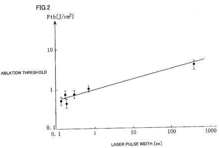
Fig. 2 shows the relationship between the laser pulse width and ablation
threshold.
BEST MODES FOR CARRYING OUT THE INVENTION
In the present embodiment, an expanded PTFE porous body, one of the organic
polymeric materials which are considered to be difficult to process with high
accuracy,
-4-
CA 02598056 2007-08-15
was selected as a material for an experiment. The expanded PTFE used for the
experiment corresponds to the material manufactured by the method described in
Japanese Patent Laying-Open No. 42-13560 and the like and is a sheet-shaped
material
of 60 m in film thickness with porosity of 60% and an average pore diameter
of 0.1 m.
The entire surface of this sheet was completely adhered to a sample holder by
means of
electrostatic force and then irradiation of a pulsed laser with laser energy
varied for
every laser pulse width was conducted. Since titanium sapphire can oscillate
laser with
the highest stability and intensity, the titaniumJsapphire laser with a
wavelength of
800nm was used. The experiment was conducted at the pulse widths of 0.135
picoseconds, 0.183 picoseconds, 0.189 picoseconds, 0.305 picoseconds, 0.7
picoseconds, and 400 picoseconds.
(Result of experiment)
(1) Shape of processing mark
Fig. I shows the relationship of the processing diameter and laser energy when
the laser was directed onto the material with the energy varying from 7.25 J
up to the
vicinity of 212 J, the pulse width of 0.135 picoseconds, the frequency of 10
Hz, and
the laser spot diameter of 44 m. Similarly in Fig. 1, a theoretical curve
based on
theoretical values of both the processing diameter and laser energy is shown
for
comparison. Note that the theoretical value is known to be expressed by the
following
formula when a space profile of the laser is of a gaussian configuration:
D = a x{ 1 n(F/F~n) }"2
Where D is a processing diameter, a is a laser spot diameter, F is laser
energy, and Fth is
an ablation threshold value. Moreover, in Fig. 1, each point shows a
measurement
point, and the horizontal and vertical line segment for each point shows an
error bar.
As clearly seen from the result of Fig. 1, the values obtained by the
experiment are close
to the theoretical values, i.e., it was confirmed that the material used for
the experiment
has been processed with a high degree of accuracy.
(2) Relationship between laser pulse width and ablation threshold
-5-
CA 02598056 2007-08-15
The relationship between laser pulse width and ablation threshold was then
evaluated. That is, referring to the fluence with the processing diameter D =
0 in Fig, 1,
the ablation threshold is 7.5 J at the laser pulse width of 0.135 picoseconds
in the case
of the material employed for the experiment, i.e., 0.5 J/cm2 when expressed in
fluence
(energy density) was obtained as a result.
Subsequently, similar experiments were conducted on the above-mentioned
materials with other laser pulse widths to confirm that a high-precision
processing had
been achieved by comparing the chart with the theoretical curve, as well as to
determine
the ablation threshold for every laser pulse width. The result is shown in
Fig. 2. In
Fig. 2, the horizontal axis indicates the laser pulse width in the logarithmic
scale by the
picosecond. Similarly, the vertical axis indicated the ablation threshold
(energy
density) in the logarithmic scale by the J/cm2. Each point shows a measurement
point,
and a vertical line segment for each point shows an error bar.
Seen from Fig. 2, the gradient of the chart expressing the relationship
between
the laser pulse width and ablation threshold was about 0.26, i.e., less than
0.5, for the
material used for the experiment, which was a moderate linear gradient.
Moreover, it
was identified that there was no rapid and distinct change in slope of the
relationship.
That is, as for the material used for the experiment, it is understood that
because of such
a relationship between laser pulse width and ablation threshold, the ablation
threshold
receives minor adverse affects even if the laser pulse width varies. Therefore
it
becomes easy to control the laser pulse width and efficiently process the
material with
high accuracy. In view of the foregoing, the gradient of the chart expressing
the
relationship between laser pulse width and ablation threshold is preferably
not more than
0.40, more preferably not more than 0.34.
The measurement points shown in Fig. 2 are for the pulse widths of 0.135
picoseconds, 0.183 picoseconds, 0.189 picoseconds, 0.305 picoseconds, 0.7
picoseconds and 400 picoseconds, and the ablation threshold for each pulse
width is
0.50 J/cmZ, 0.75 J/cm2, 0.44 J/cm2, 0.75 J/cmZ, 0.99 J/cm2, and 3.87 J/cm2,
respectively.
-6-
CA 02598056 2007-08-15
The embodiments disclosed herein should not be taken by way of limitation but
illustrative in all respects. It is intended that the scope of the present
invention be
expressed by the terms of the appended claims, rather than by the above-
mentioned
description, and all the modifications within the meaning and scope of the
claims and
their equivalents be included.
-7-