Note: Descriptions are shown in the official language in which they were submitted.
CA 02598311 2007-08-16
WO 2006/091612 PCT/US2006/006153
1
SUPERCONDUCTIVE ARTICLES HAVING DENSITY CHARACTERISTICS
TECHNICAL FIELD
The present invention is generally directed to superconductive articles. The
invention is
particularly related to superconductive articles in the form of coated
conductors and devices
incorporating the same.
BACKGROUND ART
Superconductor materials have long been known and understood by the technical
community.
Low-temperature (low-T.) superconductors exhibiting superconductive properties
at temperatures
requiring use of liquid helium (4.2 K), have been known since about 1911.
However, it was not until
somewhat recently that oxide-based high-temperature (high-T.) superconductors
have been discovered.
Around 1986, a first high-temperature superconductor (HTS), having
superconductive properties at a
temperature above that of liquid nitrogen (77 K) was discovered, namely
YBa2Cu3O7_x (YBCO),
followed by development of additional materials over the past 15 years
including BizSr2Ca2Cu3Olo+l,
(BSCCO), and others. The development of high-T, superconductors has brought
potential,
economically feasible development of superconductor components incorporating
such materials, due
partly to the cost of operating such superconductors with liquid nitrogen,
rather than the comparatively
more expensive cryogenic infrastructure based on liquid helium.
Of the myriad of potential applications, the industry has sought to develop
use of such materials
in the power industry, including applications for power generation,
transmission, distribution, and
storage. In this regard, it is estimated that the native resistance of copper-
based commercial power
components is responsible for quite significant losses in electricity, and
accordingly, the power industry
stands to gain significant efficiencies based upon utilization of high-
temperature superconductors in
power components such as transmission and distribution power cables,
generators, transformers, and
fault current interrupters. In addition, other benefits of high-temperature
superconductors in the power
industry include an increase in one to two orders of magnitude of power-
handling capacity, significant
reduction in the size (i.e., footprint) of electric power equipment, reduced
environmental impact,
greater safety, and increased capacity over conventional technology. While
such potential benefits of
high-temperature superconductors remain quite compelling, numerous technical
challenges continue to
exist in the production and commercialization of high-temperature
superconductors on a large scale.
Among the challenges associated with the commercialization of high-temperature
superconductors, many exist around the fabrication of a superconducting tape
that can be utilized for
formation of various power components. A first generation of superconducting
tape includes use of the
above-mentioned BSCCO high-temperature superconductor. This material is
generally provided in the
form of discrete filaments, which are embedded in a matrix of noble metal,
typically silver. Although
CA 02598311 2007-08-16
WO 2006/091612 PCT/US2006/006153
2
such conductors may be made in extended lengths needed for implementation into
the power industry
(such as on the order of kilometers), due to materials and manufacturing
costs, such tapes do not
represent a commercially feasible product.
Accordingly, a great deal of interest has been generated in the so-called
second-generation HTS
tapes that have superior commercial viability. These tapes typically rely on a
layered structure,
generally including a flexible substrate that provides mechanical support, at
least one buffer layer
overlying the substrate, the buffer layer optionally containing multiple
films, an HTS layer overlying
the buffer film, and an electrical stabilizer layer overlying the
superconductive layer, typically formed
of at least a noble metal. However, to date, numerous engineering and
manufacturing challenges
remain prior to full commercialization of such second generation-tapes.
Accordingly, in view of the foregoing, various needs continue to exist in the
art of
superconductors, and in particular, provision of commercially viable
superconductive tapes, methods
for forming same, and power components utilizing such superconductive tapes.
DISCLOSURE OF INVENTION
According to the first aspect of the disclosed superconductive article, a
substrate comprising
titanium is provided. A buffer layer overlies the substrate, and a
superconductive layer overlies the
buffer layer.
Another aspect provides a superconductive article having a substrate, a buffer
layer overlying
the substrate, a superconductive layer overlying the buffer layer, and a
stabilizer layer overlying the
superconductive layer. The stabilizer layer comprises aluminum.
Another aspect provides a superconductive article including a substrate having
a dimension
ratio not less than 10 and a superconductive layer overlying the substrate,
wherein the superconductive
article has a density not greater than about 7.OOg/cc.
Another aspect provides a superconductive article including a substrate having
a density not
greater than about 8.OOg/cc, a buffer layer overlying the substrate and a
superconductive layer
overlying the substrate. Generally, the article has a dimension ratio not less
than about 10.
Another embodiment of the device provides a substrate, a buffer layer
overlying the substrate, a
superconductive layer overlying the substrate, and a stabilizer layer
overlying the superconductive
layer having a density not greater than about 8.OOg/cc.
BRIEF DESCRIPTION OF THE DRAWINGS
Fig. 1 illustrates a perspective view of the layers of the superconductive
article for one
embodiment.
CA 02598311 2007-08-16
WO 2006/091612 PCT/US2006/006153
3
Fig. 2 illustrates a schematic view of a transformer.
Fig. 3 illustrates a schematic view of a power generator.
MODES FOR CARRYING OUT THE INVENTION
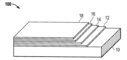
Fig. 1 illustrates the layered structure of a superconductive article 100
according to one
embodiment. The superconductive article includes a substrate 10, a buffer
layer 12, and a
superconductive layer 14. A capping layer 16 may be provided overlying the
superconductive layer,
followed by a stabilizer layer 18 overlying the capping layer 16.
The substrate is generally formed of a material able to withstand the
mechanical stress and
strain of reel-to-reel processing and may also provide mechanical integrity
for the final
superconductive article in a variety of applications. Further, the substrate
may advantageously
withstand high processing temperatures and aggressive processing environments
(e.g., highly
oxidative) that are utilized during fabrication of the superconductive
article. In view of the foregoing,
the substrate 10 is generally metal-based, and typically, an alloy of at least
two metallic elements.
Suitable substrate materials include nickel-based metal alloys such as the
known Inconel group of
alloys. Of available materials, nickel-based metal alloys such as the Inconelg
group of alloys tend to
have desirable creep, chemical and mechanical properties, including
coefficient of expansion, tensile
strength, yield strength, and elongation. However, in one particular
embodiment, the substrate 10 is
comprised comparatively lower mass density materials. In this respect, the
substrate 10 may have a
mass density not greater than about 8.OOg/cc, such as not greater than about
7.OOg/cc or 6.OOg/cc. In
some instances the mass density of the substrate is not greater than about
5.OOg/cc.
In the context of low mass density material substrates, use may be made of
titanium metal or a
titanium metal alloys. Useful alloying metal elements include aluminum,
vanadium, iron, tin,
ruthenium, palladium, zirconium, molybdenum, nickel, niobium, chromium and
silicon, and
combinations thereof. Of these, particularly useful alloying elements include
aluminum and vanadium.
In one embodiment, aluminum and vanadium are present, in amounts not greater
than 10% and 8% by
weight, respectively, such as not greater than 6% and 4% by weight
respectively. One particular
species is Grade 9 titanium alloy, containing 3% aluminum and 2.5% vanadium by
weight, the balance
being titanium. The particular selection of alloying elements may depend upon
various factors,
including oxidation resistance characteristics.
In the particular context of titanium alloys, the total weight percent of
alloying metal elements
of the substrate 10 is generally not greater than about 20%, most often not
greater than 10% by weight,
and the percentage of titanium is not less than about 80% by weight and in
other embodiments the
titanium is not less than about 85% or 90% by weight. Titanium and titanium
alloys desirably provide
a substrate having a mass density not greater than about 5.0 g/cc, such as
within a range of about 4.0 to
5.0 g/cc.
CA 02598311 2007-08-16
WO 2006/091612 PCT/US2006/006153
4
Further, according to embodiments herein, the substrate 10 may be resistive to
enable reduction
in eddy current losses in the superconductive layer. Such reduction in eddy
current losses is
particularly beneficial when the article takes the form of a rotating machine,
such as a power generator
or motor (further described below). Use of resistive substrates minimizes ac
losses when deployed in
the form of a rotating machine. Typical resistivities of the substrate are
generally greater than about 50
micro-ohm cm, such as greater than about 100 micro-ohm cm.
Further, the thickness of the substrate may be reduced according embodiment
while still
providing adequate to withstand reel-to-reel processing, handling, and
integrity in the field. Typically,
the substrate 10 has a thickness not greater than about 50 microns, or even
not greater than 40 microns.
Still, in other embodiments, the thickness of the substrate 10 may be not
greater than about 30 microns
or even as thin as about 20 microns or less.
The substrate 10 generally is a tape, having a high dimension ratio. As used
herein, the term
'dimension ratio' is used to denote the ratio of the length of the substrate
10 or tape to the next longest
dimension, the width of the substrate 10 or tape. For example, the width of
the substrate ranges
approximately from 0.4 -10cm and the length of the substrate 10 is typically
greater than about 100m,
oftentimes greater than about 500m. Indeed, one embodiment provides for
superconductive substrates
having a length on the order of Ikm or above, which may comprise multiple tape
segments.
Accordingly, the substrate may have a dimension ratio which is fairly high, on
the order of not less than
10, not less than about 102, or even not less than about 103. Certain
embodiments are longer, having a
dimension ratio of 104 and higher.
In one embodiment, the substrate 10 is treated so as to have desirable surface
properties for
subsequent deposition of the constituent layers of the superconductive
article. For example, the surface
may be lightly polished to a desired flatness and surface roughness.
Additionally, the substrate 10 may
be treated to be biaxially textured as is understood in the art, such as by
the known RABiTS (roll
assisted biaxially textured substrate) technique, although generally
embodiments herein take advantage
of non-textured substrates, particularly including metal alloy polycrystalline
substrates.
Turning back to FIG. 1, the illustrated embodiment provides a buffer layer 12.
The buffer layer
may be a single layer, or more commonly, be made up of several films. Most
typically, the buffer layer
12 includes a biaxially textured film, having a crystalline texture that is
generally aligned along crystal
axes both in-plane and out-of-plane of the film. The biaxial texturing of the
buffer layer 12 may be
accomplished by IBAD. As is understood in the art, IBAD is acronym that stands
for ion beam assisted
deposition, a technique that may be advantageously utilized to form a suitably
textured buffer layer for
subsequent formation of a superconductive layer having desirable
crystallographic orientation for
superior superconducting properties. Magnesium oxide is a typical material of
choice for the IBAD
film, and may be on the order or 50 to 500 Angstroms, such as 50 to 200
Angstroms. Generally, the
IBAD film has a rock-salt like crystal structure, as defined and described in
US Patent 6,190,752,
incorporated herein by reference.
CA 02598311 2007-08-16
WO 2006/091612 PCT/US2006/006153
The buffer layer 12 may include additional films, such as a barrier film
provided in between an
IBAD film and the substrate 10. In this regard, the barrier film 12 may
advantageously be formed of an
oxide, such as yttria, and functions to isolate the substrate from the IBAD
film. A barrier film 12 may
also be formed of non-oxides such as silicon nitride. Suitable techniques for
deposition of a barrier
5 film include chemical vapor deposition and physical vapor deposition
including sputtering. Typical
thicknesses of the barrier film may be within a range of about 100-200
Angstroms. Still further, the
buffer layer may also include an epitaxially grown film, formed over the IBAD
film. In this context,
the epitaxially grown film is effective to increase the thickness of the IBAD
film, and may desirably be
made principally of the same material utilized for the IBAD layer such as MgO.
In embodiments utilizing an MgO-based IBAD film and/or epitaxial film, a
lattice mismatch
between the MgO material and the material of the superconductive layer may
exist. Accordingly, the
buffer layer 12 may further include another buffer film, this one in
particular implemented to reduce a
mismatch in lattice constants between the superconductive layer and the
underlying IBAD film and/or
epitaxial film. This buffer film may be formed of materials such as YSZ
(yttria-stabilized zirconia)
strontium ruthenate, lanthanum manganate, and generally, perovskite-structured
ceramic materials.
The buffer film may be deposited by various physical vapor deposition
techniques, and generally
retains the biaxial texture of the underlying layer on which it is formed.
The superconductive layer 14 is generally in the form of a high-temperature
superconductor
(HTS) layer. HTS materials are typically chosen from any of the high-
temperature superconducting
materials that exhibit superconducting properties above the temperature of
liquid nitrogen, 77K. Such
materials may include, for example, YBa2Cu3O7_X, Bi2Sr2CaZCu3Ojo+y,
Ti2Ba2CazCu3O1 o+Y, and HgBa2
Ca2Cu3 O8+Y. One class of materials includes REBa2Cu3O7_X, wherein RE is a
rare earth element. Of
the foregoing, YBa2Cu3O7,, also generally referred to as YBCO, may be
advantageously utilized. The
superconductive layer 14 may be formed by any one of various techniques,
including thick and thin
film forming techniques. Preferably, a thin film physical vapor deposition
technique such as pulsed
laser deposition (PLD) can be used for a high deposition rates, or a chemical
vapor deposition
technique can be used for lower cost and larger surface area treatment.
Typically, the superconductive
layer has a thickness on the order of about i to about 30 microns, most
typically about 2 to about 20
microns, such as about 2 to about 10 microns, in order to get desirable
amperage ratings associated
with the superconductive layer 14.
The stabilizer layer 18 and capping layer 16 (optional) are generally
implemented to provide a
low resistance interface for electrical stabilization to aid in prevention of
superconductor burnout in
practical use. More particularly, stabilizer layer 18 aids in continued flow
of electrical current along
the superconductive conductor in cases where cooling fails or the critical
current density is exceeded,
and the superconductive layer becomes non-superconductive. The capping layer
16 may be
incorporated in the structure particularly for those embodiments where
undesirable interaction between
the superconductive layer 14 and the stabilizer layer 18 would otherwise take
place. In such cases, the
capping layer may be formed of a noble metal, such as gold, silver, platinum,
and palladium. Silver is
CA 02598311 2007-08-16
WO 2006/091612 PCT/US2006/006153
6
typically used due to its cost and general accessibility. The capping layer 16
is typically made to be
thick enough to prevent unwanted diffusion of the components from the
stabilizer layer 18 into the
superconductive layer 14, but is made to be generally thin for cost reasons
(raw material and processing
costs). Typical thicknesses of the capping layer 16 range within about 0.1 to
about 10.0 microns, such
as 0.5 to about 5.0 microns. Various techniques may be used for deposition of
the capping layer 16,
including physical vapor deposition, such as DC magnetron sputtering.
The stabilizer layer 18 is generally incorporated to overlie the
superconductive layer 14, and in
particular, overlie and directly contact the capping layer 16 in the
particular embodiment shown in Fig.
1, although elimination of the capping layer would result in direct contact
with the superconductive
layer 14 according to an alternate embodiment. The stabilizer layer 18
functions as a protection/shunt
layer to enhance stability against harsh environmental conditions and
superconductivity quench. The
layer is generally thermally and electrically conductive, and functions to
bypass electrical current in
case of failure of the superconductive layer. It may be formed by any one of
various thick and thin film
forming techniques, such as by laminating a pre-formed copper strip onto the
superconductive tape, by
using an intermediary bonding material such as a solder or flux. Other
techniques have focused on
physical vapor deposition, typically evaporation or sputtering, as well as wet
chemical processing such
as electroless plating, and electroplating.
Typically, metals such as copper are used for the stabilizer layer 18.
However, according to
other embodiments, the stabilizer layer utilizes lower density materials, such
as materials having a mass
density less than about 8.OOg/cc, 7.OOg/cc, or even 6.00g/cc. Indeed, certain
embodiments have
stabilizer layers that have a density not greater than about 4.OOg/cc or not
greater than about 3.OOg/cc.
According to a particular embodiment a comparatively low density conductive
metal such as aluminum
forms the major component (greater than 50% by weight) of the stabilizer layer
18. For example, the
stabilizer layer 18 may be aluminum or an aluminum metal alloy in which
aluminum is present in at
least about 80% by weight. The use of aluminum not only reduces the density of
the stabilizer layer
18, but notably the global density of the superconductive article 100. Use of
aluminum-based materials
provides for stabilizer layers having desirably low mass densities, such as
not greater than about 3.00
g/cc, =such as within a range of about 2.00 to 3.00 g/cc.
Typically, the thickness of the stabilizer layer is not less than about 50
microns, oftentimes not
less than about 100 microns. Of note, aluminum-based stabilizers may be
comparatively thicker than
copper-based stabilizers having the same current carrying capability, since
aluminum has a higher
resistivity than copper. Despite a relative increase in thickness associated
with aluminum-based
stabilizers, the mass of the superconductor article may still be reduced due
to a significant reduction in
mass density.
While the density of materials comprising particular layers has been described
above, the global
density of the entire superconductive article is desirably reduced according
to embodiments herein. A
less dense superconductive article may be advantageous for rotating machine
applications, such as
CA 02598311 2007-08-16
WO 2006/091612 PCT/US2006/006153
7
generators, that place a significant force on, for example, a coil of
superconductive tape. Accordingly,
in some embodiments a global density of the superconductive article may be
less than about 7.OOg/cc.
While other embodiments make use of global densities less than about 6.50g/cc,
6.OOg/cc or even
5.OOg/cc. A lower global density is achieved by reducing the density of each
of the component layers,
notably the substrate and stabilizer layers as previously detailed.
While a generalized structure of a superconductor article has been described
above in
connection with Fig. 1, additional embodiments are illustrated in Figs. 2 and
3, which show typical
applications for a superconductive tape or superconductive article having a
high dimension ratio.
Beyond the particular architecture and in connection with superconductive
articles or tapes as described
above in connection with Fig. 1, embodiments are also directed to components,
such as industrial or
commercial power components incorporating such conductors. Certain classes of
such components
incorporate coils or windings of high dimension ratio superconductive
conductors and are of particular
significance. Within the context of coiled or wound architectures, certain
embodiments are drawn to a
class of power components known as 'rotating machines,' which broadly includes
power generators
and motors. Such structures implement coiled high dimension ratio
superconductive conductors that
are rotated at high speeds. Embodiments herein having low density substrates,
low density stabilizers,
and/or low global density find particular use in such rotating machines.
For example, Fig. 2 illustrates a power transformer having a central core 76
around which a
primary winding 72 and a secondaiy winding 74 are provided. It is noted that
Fig. 2 is schematic in
nature, and the actual geometric configuration of the transformer may vary as
is well understood in the
art. However, the transformer includes at least the basic primary and
secondary windings. In this
regard, in the embodiment shown in Fig. 2, the primary winding has a higher
number of coils than the
secondary winding 74, representing a step-down transformer that reduces
voltage of an incoming
power signal. In reverse, provision of a fewer number of coils in the primary
winding relative to the
secondary winding provides a voltage step-up. In this regard, typically step-
up transformers are
utilized in power transmission substations to increase voltage to high
voltages to reduce power losses
over long distances, while step-down transformers are integrated into
distribution substations for later
stage distribution of power to end users. At least one of and preferably both
the primary and secondary
windings comprise superconductive tapes in accordance with the foregoing
description.
Turning to Fig. 3, a schematic illustration of a generator is provided. The
generator includes a
rotor 86 that is driven, as is known in the art, by a turbine. Rotor 86
includes high-intensity
electromagnets, which are formed of rotor coils 87 that form the desired
electromagnetic field for
power generation. The generation of the electromagnetic field generates power
in the stator 88, which
comprises at least one conductive stator winding 89. According to a particular
feature, the rotor coils
87 and/or the stator winding 89 comprises a superconductive article in
accordance with embodiments
described above.
CA 02598311 2007-08-16
WO 2006/091612 PCT/US2006/006153
8
According to various embodiments described above, superconductor articles
having desirable
mass density characteristics are provided. Such superconductor articles may
provide improved
mechanical integrity and robustness, particularly when used in highly dynamic
environments such as
rotating machines, at least partially due to the reduced mass density of the
articles.
While particular aspects of the present invention have been described herein
with particularity,
it is well understood that those of ordinary skill in the art may make
modifications hereto yet still be
within the scope of the present claims. The previously mentioned embodiments
and examples, in no
way limit the scope of the following claims.