Note: Descriptions are shown in the official language in which they were submitted.
CA 02598490 2011-08-08
.=
THREE DIMENSIONAL MULTI-JUNCTION PHOTOVOLTAIC DEVICE
BACKGROUND
[002] Photovoltaic solar cells tap the sun's limitless energy. Tapping such a
limitless energy source could remedy the world's many energy dilemmas.
Photovoltaic cells, for example, absorb energy from light and convert the
absorbed
energy to an electrical current. As shown in FIG. 1, in a conventional (e.g.
planar)
single-junction solar cell 100, a light photon 105 from sun 110 impinges a p/n-
junction 115 at a single instance. This impingement creates a single electron-
hole
pair in p/n-junction 115. However, as shown in FIG. 1, unabsorbed photons 120
reflect into the atmosphere or space.
[003] Conventional single solar cells are typically small wafers
approximately six inches across. These solar cells may be first arranged into
modules and then large photovoltaic arrays that may cover dozens of square
meters
in order to satisfy specific power needs.
[004] Thus, the conventional strategy is to absorb energy from light photons
that impinge a solar cell at a single impingement instance. Then energy from
this
single impingement is then converted to an electrical current by the solar
cell. This
often causes problems because the conventional strategy absorbs only a small
amount of the available energy. For example, the conventional strategy
reflects
unabsorbed energy into the atmosphere or space.
SUMMARY
[005] A three dimensional multi-junction photovoltaic device may be
provided. This Summary is provided to introduce a selection of concepts in a
1
CA 02598490 2007-11-15
simplified form that are further described below in the Detailed Description.
This
Summary is not intended to identify key features or essential features of the
claimed
subject matter. Nor is this Summary intended to be used to limit the scope of
the
claimed subject matter.
[006] In accordance with one embodiment, a photovoltaic device may
comprise a first energy absorbing element configured to convert energy from a
photon
impinging the first energy absorbing element into a first electrical current.
Furthermore, the photovoltaic device may comprise a second energy absorbing
element being oriented with the first energy absorbing element in a non-
parallel
manner. The second energy absorbing element may be configured to convert
energy
from the photon impinging the second energy absorbing element into a second
electrical current. The photon impinging the second energy absorbing element
may do
so after the photon impinged the first energy absorbing element.
[007] According to another embodiment, a photovoltaic device may comprise
a first energy absorbing surface and a second energy absorbing being
substantially
parallel to the first energy absorbing surface. The photovoltaic device may
further
comprise a third energy absorbing surface being substantially perpendicular to
the first
energy absorbing surface and the second energy absorbing surface. Each of the
first
energy absorbing surface, the second energy absorbing surface, and the third
energy
absorbing surface may be configured to convert energy from photons into
electrical
energy. The photons may be impinging one or more of the first energy absorbing
surface, the second energy absorbing surface, and the third energy absorbing
surface.
The first energy absorbing surface, the second energy absorbing surface, and
the third
energy absorbing surface may be oriented in manner to cause the photons to
bounce
between two or more of the first energy absorbing surface, the second energy
absorbing surface, and the third energy absorbing surface.
[008] In accordance with yet another embodiment, a method for providing a
photovoltaic device may comprise providing a substrate comprising a third
energy
absorbing surface. The method may further comprise providing a first carbon
nanotube on the substrate and providing a second carbon nanotube on the
substrate.
In addition, the method may include coating the first carbon nanotube with a
first
energy absorbing surface and coating the second carbon nanotube with a second
energy absorbing surface. Each of the first energy absorbing surface, the
second
2
CA 02598490 2007-11-15
energy absorbing surface, and the third energy absorbing surface may be
configured
to convert energy from photons into electrical energy. The photons may be
impinging one or more of the first energy absorbing surface, the second energy
absorbing surface, and the third energy absorbing surface. The first energy
absorbing surface, the second energy absorbing surface, and the third energy
absorbing surface may be oriented in manner to cause the photons to bounce
between
two or more of the first energy absorbing surface, the second energy absorbing
surface, and the third energy absorbing surface.
[009] Both the foregoing general description and the following detailed
description provide examples and are explanatory only. Accordingly, the
foregoing
general description and the following detailed description should not be
considered
to be restrictive. Further, features or variations may be provided in addition
to those
set forth herein. For example, embodiments may be directed to various feature
combinations and sub-combinations described in the detailed description.
BRIEF DESCRIPTION OF THE DRAWINGS
[010] The accompanying drawings, which are incorporated in and constitute
a part of this disclosure, illustrate various embodiments of the present
invention. In
the drawings:
[011] FIG. 1 is a block diagram of a photovoltaic device;
[012] FIG. 2 is a block diagram of a three dimensional photovoltaic device;
[013] FIG. 3 is a diagram showing a three dimensionally aligned array of
carbon nanotube (CNT) towers grown on a lithographically patterned wafer;
[014] FIG. 4 is a diagram showing a three dimensional multi-junction
photovoltaic device;
[015] FIG. 5 is a diagram showing a three dimensional multi-junction
photovoltaic device;
[016] FIG. 6 is a graph illustrating light absorption; and
[017] FIG. 7 is another graph illustrating light absorption.
DETAILED DESCRIPTION
[018] The following detailed description refers to the accompanying
drawings. Wherever possible, the same reference numbers are used in the
drawings
3
CA 02598490 2007-11-15
and the following description to refer to the same or similar elements. While
embodiments of the invention may be described, modifications, adaptations, and
other implementations are possible. For example, substitutions, additions, or
modifications may be made to the elements illustrated in the drawings, and the
methods described herein may be modified by substituting, reordering, or
adding
stages to the disclosed methods. Accordingly, the following detailed
description
does not limit the invention. Instead, the proper scope of the invention is
defined by
the appended claims.
[019] Photovoltaic solar cells tap the sun's limitless energy. Tapping such a
limitless energy source could remedy the world's many energy dilemmas.
Photovoltaic cells, for example, absorb energy from light and convert the
absorbed
energy to an electrical current. Multi-junction photovoltaic devices,
consistent with
embodiments of the invention, may comprise carbon nanotube (CNT) based
photovoltaic cells that demonstrate efficiencies that exceed 50%. The
aforementioned photovoltaic cells may comprise a small "footprint" due, for
example, to the nanostructured topography of the photoactive surface.
Photovoltaic
devices, consistent with embodiments of the invention, maybe light weight that
may
make them extremely beneficial for space applications where launch mass may be
a
major cost driver.
[020] An embodiment consistent with the invention may comprise a three
dimensional photovoltaic device. The photovoltaic device may comprise a first
energy absorbing element configured to convert energy from a photon impinging
the
first energy absorbing element into a first electrical current. Furthermore,
the
photovoltaic device may comprise a second energy absorbing element being
oriented
with the first energy absorbing element in a non-parallel manner. The second
energy
absorbing element may be configured to convert energy from the photon
impinging
the second energy absorbing element into a second electrical current. The
photon
impinging the second energy absorbing element may do so after the photon
impinged
the first energy absorbing element.
[021] Another embodiment consistent with the invention may comprise a
photovoltaic device. The device may comprise a first energy absorbing surface
and a
second energy absorbing being substantially parallel to the first energy
absorbing
surface. The photovoltaic device may further comprise a third energy absorbing
4
CA 02598490 2007-11-15
surface being substantially perpendicular to the first energy absorbing
surface and
the second energy absorbing surface. Each of the first energy absorbing
surface, the
second energy absorbing surface, and the third energy absorbing surface may be
configured to convert energy from photons into electrical energy. The photons
may
be impinging one or more of the first energy absorbing surface, the second
energy
absorbing surface, and the third energy absorbing surface. The first energy
absorbing surface, the second energy absorbing surface, and the third energy
absorbing surface may be oriented in manner to cause the photons to bounce
between
two or more of the first energy absorbing surface, the second energy absorbing
surface, and the third energy absorbing surface.
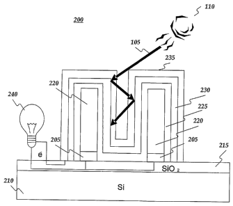
[022] FIG. 2 is a block diagram of a photovoltaic device 200 consistent with
an embodiment of the invention. As shown in FIG. 2, catalyst metal sites 205
(e.g.,
Fe) maybe deposited onto a silicon substrate 210 having an oxidized layer 215.
CNT
towers 220, composed, for example, of millions of CNTs, maybe grown atop
catalyst
metal sites 205. CNT towers 220 may serve as a back contact for photovoltaic
device 200. In other words, CNT towers 220 may serve as electrical conductors
for
electrical current produced by photovoltaic device 200. Sequential deposition
of a
first photoactive material 225 and a second photoactive material 230 may
create, for
example, a p/n-junction. The p/n-junction may comprise an energy absorbing
element or layer configured to convert energy from a photon impinging the
energy
absorbing layer into electrical energy. A transparent conductive oxide (TCO)
235
may serve as the top contact for photovoltaic device 200. Photovoltaic device
200
may supply electrical energy to a load 240. As described in more detail below,
consistent with embodiments of the invention, the energy absorbing layer may
comprise, for example, cadmium telluride (CdTe/CdS). Embodiments of the
invention, however, are not limited to CdTe and other materials may be used.
In
conventional systems, (e.g. single-junction solar cell 100) a light photon
impinges,
for example, a p/n-junction at a single instance and creates a single electron-
hole
pair. Then, any unabsorbed photons reflect into the atmosphere or space.
Consistent
with embodiments of the invention, however, multiple photon impingements upon
photovoltaic device 200 allowing more photon energy absorption and can improve
conversion efficiencies using a "light trapping" effect.
5
CA 02598490 2007-11-15
[023] FIG. 3 is a diagram showing a three dimensionally aligned array 300
of CNT towers 305 grown on a lithographically patterned silicon (Si) wafer 310
consistent with an embodiment of the invention. Conductive CNT array 300 may
then be coated with a suitable photon absorbing band gap materials (e.g.
CdTe/CdS)
to form, for example, a p/n-junction. A conductive oxide such as indium tin
oxide
(ITO) may then be deposited as the transparent top contact over the photon
absorbing
band gap materials. While FIG. 3 shows CNT towers 305 having a square shape,
embodiments of the invention are not limited to this shape and may comprise
any
shape. Consistent with another embodiment of the invention, another three
dimensionally aligned array (not shown) may comprise a relief of three
dimensionally aligned array 300. For example, rather than being grown in the
positions shown in FIG. 3, the CNTs may be grown in the space shown between
the
towers shown in FIG. 3. This relief of three dimensionally aligned array 300
may be
similar to a multi-junction photovoltaic device 500 described below with
respect to
FIG. 5.
[024] Consistent with embodiments of the invention, due to a three
dimensional nanoscale topography approach, CNT-based photovoltaic devices may
include orders of magnitude more surface area for an equivalent footprint
compared
to a conventional solar cell. For example, on each square centimeter of
substrate
supporting array 300 in FIG. 3, there may be 40,000 square CNT towers. If the
CNT
towers are grown on the substrate to be approximately 300 gm tall (e.g. CNT
growth
time of approximately 15 minutes), a p/n-junction surface area, for example,
becomes approximately 20cm2. In other words, consistent with embodiments of
the
invention, an increase in an electron-hole pair generating surface area of
2,000%
(1m2 = 10,000 cm2) may be realized with no net increase in "footprint."
Although
only a portion of the surface area may be available for an incident photon,
once a
reflection occurs, a "backside" p/n-junction of the tower, for example, maybe
available to enable multiple photon impingements (i.e. "light trapping") as
discussed
above.
[025] For a planar (i.e. one-dimensional) solar cell, performance may be
maximized when photons from the sun impinge upon a p/n-junction
perpendicularly.
At angles away from normal, a cosine term may be used to account for the less
than
optimum angle of incidence of the photon upon the p/n-junction. Some systems
use
6
CA 02598490 2007-11-15
complicated mechanical systems to maintain this orthogonal arrangement of
solar
flux to the solar cell surface. Consistent with embodiments of the invention,
a CNT-
based structure may not follow these conventional concepts. For example, a
perpendicular arrangement may minimize the amount of photon bounces and
decrease light trapping. Off-axis photon impingement at a glancing angle may
enable the photon to experience multiple bounces upon the p/n-junction.
Consequently, absorption likelihood may be increased, thus increasing
conversion
efficiency.
[026] FIG. 4 is a diagram showing a three dimensional multi-junction
photovoltaic device 400 consistent with an embodiment of the present
invention. For
example, a multi-junction device may include a planar device serving as bottom
cell
405 and a p/n-coated CNT array 410 as a top cell. CNT towers in CNT array 410
may serve as a common terminal between bottom cell 405 and CNT array 410.
Multi-junction photovoltaic device 400 enhances the "light-trapping" effect
because
the bottom cell may have a greater opportunity to absorb any "bounced" photons
from CNT array 410. Furthermore, a fraction of the solar cell that was covered
with
opaque bus-bars in conventional systems (e.g. approximately 8% of the planar
area)
may be made photoactive, thus increasing power generation, for example,
through
increased p/n-junction surface area.
[027] FIG. 5 is a diagram showing a three dimensional multi-junction
photovoltaic device 500. Three dimensional multi-junction photovoltaic device
500
maybe similar to photovoltaic device 200 shown in FIG. 2. However, as shown in
FIG. 5, Si layer 210 may be exposed to impinging photons bouncing between CNT
towers 220. In other words, photons may impinge both a first energy absorbing
surface (e.g. a first junction) on CNT towers 220 to produce electrical energy
and a
second energy absorbing surface (e.g. a second junction) on Si layer 210 to
produce
electrical energy. For example, a photon may impinge a p/n-junction at a
single
instance on either of CNT towers 220 to create a single electron-hole pair.
Then, any
unabsorbed photons may be reflected and may eventually impinge Si layer 210.
Si
layer 210 and CNT towers 220 may have different band gap values. For example,
CNT towers 220 may comprise CdTe and Si layer 210 may comprise Si.
[028] Consistent with embodiments of the invention, the first energy
absorbing surface (e.g. a first junction) and the second energy absorbing
surface (e.g.
7
CA 02598490 2007-11-15
a second junction) may be "tuned" to different photon energies. For example, a
photon, in order to create an electron on an energy absorbing surface, must
have a
certain energy level. In other words, energy absorbing surfaces have a band
gap.
Impinging photons, having an energy level above the energy absorbing surface's
band gap, create an electron. Impinging photons, having an energy level below
the
energy absorbing surface's band gap, do not create an electron. CdTe may have
a
band gap of 1.53 electron volts (eV). Any photons having energy greater than
1.53
eV may excite an electron in a CdTe energy absorbing surface and may allow the
excited electron to conduct. Silicon, on the other hand, may have a lower band
gap
of about 1.1 eV.
[029] As shown in FIG. 5, photons may first impinge CNT towers 220
including a first energy absorbing surface that has a first band gap value.
Then, the
photons may impinge Si layer 210 including a second energy absorbing surface
that
has a second band gap value. The second band gap value may be smaller than the
first band gap value. Materials with smaller band gap values may be more
expensive
and more difficult to construct. Consequently, a multi-junction photovoltaic
device
can be constructed to allow photons to first impinge the first energy
absorbing
surface and then allow reflected photons to impinge the second energy
absorbing
surface having a band gap lower that the first energy absorbing surface. In
this way,
multi-junction photovoltaic devices can use a less expensive easier to
manufacture
material to serve as the first energy absorbing surface. Photons that may not
create
electrons in the first energy absorbing surface may then be reflected to the
second
energy absorbing surface having a lower band gap in order to take advantage of
the
reflected photons' energy. Accordingly, consistent with embodiments of the
invention, multiple photon impingements upon photovoltaic device 500 allow
more
photon energy absorption and can improve conversion efficiencies using a
"light
trapping" effect on multiple junctions.
[030] As referenced above, CdTe may serve as the p-type material selected
for use in a photovoltaic device consistent with embodiments of the invention
(e.g.
Eg = 1.53eV). Molecular beam epitaxy (MBE) may be used to deposit a layer of
multicrystalline CdTe. Layer thickness for optimum photon capture and carrier
extraction may comprise 2 to 4 gm. The CNT towers described above may have
approximately 4 gm thick CdTe coatings along the walls (where the bulk of the
8
CA 02598490 2007-11-15
surface area is contained) and 10 gm on the "roof of the tower. This
difference may
be due to a physical alignment between an evaporative source material and a
substrate in an MBE chamber. Techniques such as rotating a sample at an offset
angle may improve thickness uniformity between sidewall and top surfaces.
Thickness reductions (e.g. to 2 gm) may be accomplished through reduced time
in
the MBE.
[031] CdS (Eg = 2.5eV) may serve as an n-type material. It can be applied
via chemical bath deposition (CBD) or MBE. Both techniques have advantages and
disadvantages for potential insertion into an economically viable technology.
The
ideal thickness of the CdS coating may be 50 to 150 nm. CdSe (Eg = 1.7eV) can
also
be used as a photoactive material. The technique for applying the CNTs with
CdSe
may be a solution-based technique under commercial development by Flood of
NewCyte, Inc., Oberlin, OH. CdSe could be used for a multi-junction device
where
the CdSe coated CNTs serve as the top cell gown on bus-bars while the bottom
cell
could be polysilicon cells (Eg = 1.1 eV). The bandgap pairing between CdSe and
Si
may be efficient in a multi-junction device. Moreover, as described above,
indium
tin oxide (ITO) may be applied to photovoltaic device consistent with
embodiments
of the invention. For example, ITO maybe used to form a transparent top
contact.
Evaporative and solution-based techniques to deposit the ITO onto the 3-D
arrayed
structure may be used.
[032] FIG. 6 and FIG. 7 illustrate a high photon absorbing capacity of a
photovoltaic device consistent with embodiments of the present invention. As
shown in FIGS. 6 and 7, reflectance measurements may be taken on a variety of
coated devices as described above. As shown in FIG. 6, an Si cell may exhibit
significant reflection and thus allows for wasted photons. As shown in FIG. 7,
an
expansion of the scale shows that reflectance from photovoltaic devices
consistent
with embodiments of the present invention maybe less than 1.5%, thus
demonstrating the light trapping concept described above.
[033] Consistent with embodiments of the invention, CNT tower shape may
be optimized. For example, a square structure may not be ideal for optimum
reflection and light trapping. A multi-faceted CNT tower (i.e., star shaped)
may
have greater surface area and may offer enhanced light trapping capabilities.
Furthermore, a CNT cylindrical tower may allow for uniformity and less
internal
9
CA 02598490 2007-11-15
stress within p/n-type materials. These stresses could induce dislocations
that may
serve as recombination centers for electron-hole pairs and could degrade
photovoltaic device efficiency.
[034] Consistent with embodiments of the invention, p/n-type layers may be
optimized. For example, with any photoactive material, performance gains may
be
realized by maximizing both photon absorption and electron-hole carrier
extraction.
CdTe may be used as the p-type material and CdS as the n-type material. Grain
refinement and annealing of the CdTe structure may be important to prevent
inadvertent electron-hole recombination. One of the principal processes for
CdTe
gain refinement may be via CdC12 treatment and thermal annealing. This
compound
may be used in a CBD process for CdS application. In addition, a hexagonal CNT
structure may encourage preferential growth of the hexagonal close packed
(HCP)
structure for the CdTe.
[035] The use of MBE may have a line-of-sight limitation in creating
uniform top and sidewall thicknesses. Implementation of a rotating and
slightly
angled substrate holder could allow more uniform coverage of the evaporated
material. In addition, the CdTe thin film thickness optimization may be based
on
calculations for planar structures. Embodiments of the invention may have a
different optimized thickness for CdTe to allow for maximized photon
absorption
and carrier extraction.
[036] In addition, consistent with embodiments of the invention, other p/n-
type materials may be used, for example, doped-Si, InGaP, GaAs, GaN, CdSe,
CIGS, and CIS. The aforementioned p/n-type materials are examples, and others
may be used. The use of other p/n-type materials may be used for outer space
applications where radiation effects upon thin film generate defects that may
degrade
performance over time. Furthermore, consistent with embodiments of the
invention,
because certain CNTs may be semiconducting, the p/n-type material may be
eliminated entirely and the CNT array itself may be used as both the photon
absorbing band gap material and the carrier conducting material.
[037] Consistent with embodiments of the invention a top contact of a
photovoltaic device may be optimized. For example, the ITO top contact that
serves
as the TCO may be optimized. This contact may offer high conductivity with
underlying photoactive layers to extract the carriers before recombination can
occur.
CA 02598490 2007-11-15
In addition, very low series resistance and high optical transmission may be
required
so that it affords little impediment to charge carrier transport or photon
absorption.
Other top contact materials could also be used. For example, if CdSe were used
as
the photoactive species, it could be paired with SnO. This combination may
offer a
simplified layering and a more efficient structure resulting from alignment of
the
SnO Fermi level with the CdSe conduction band edge.
[038] Consistent with embodiments of the invention, a bottom contact of a
photovoltaic device may be optimized. The bottom contact may be formed by a
CNT tower. The bottom contact resistance losses may degrade efficiency. These
contact losses may be between the band gap material and the CNT or between the
CNT and the metallic circuit contact on the substrate. Embodiments of the
invention
may minimize these losses.
[039] The CNT tower may be composed of 100% "arm-chair" single wall
carbon nanotubes (SWNTs) that may offer high efficiency "ballistic" conduction
to
extract carriers from overlying photoactive materials. Attaining chairal
control may
be difficult, thus a statistical blend of arm chair, "zigzag," and other
semiconducting
CNTs with varying band gaps may be generated. Consistent with embodiments of
the invention, for example, this effect may be overcome by using a multitude
(many
millions) of CNTs aligned in parallel to form each tower. The multiplicity of
parallel
conduction paths may overwhelm the losses that may result from the
semiconducting
CNTs.
[040] Furthermore, the band gap of the semiconducting CNTs may be
tailored to allow photon absorption and thereby may serve as a substitute for
p/n-type
layers. From a production economics standpoint, the elimination of the p/n-
type
layering processes may allow for more economic designs and manufacturing
processes. Furthermore, consistent with embodiments of the invention, if the
periodicity of a nanotube patterns is tuned to a resonant frequency of the
incident
light, a photonic crystal may be generated. Consequently, a photon's wave-like
properties may be exploited. Accordingly, absorption and light trapping may be
further enhanced.
[041] While certain embodiments of the invention have been described,
other embodiments may exist. Further, the disclosed methods' stages may be
modified in any manner, including by reordering stages and/or inserting or
deleting
11
CA 02598490 2007-11-15
=
stages, without departing from the invention. While the specification includes
examples, the invention's scope is indicated by the following claims.
Furthermore,
while the specification has been described in language specific to structural
features
and/or methodological acts, the claims are not limited to the features or acts
described above. Rather, the specific features and acts described above are
disclosed
as example for embodiments of the invention.
12