Note: Descriptions are shown in the official language in which they were submitted.
CA 02599246 2007-09-12
Doc. No.: 18-32 CA/PCT DIV Patent
DIFFRACTIVE SURFACES WITH COLOR SHIFTING BACKGROUNDS
BACKGROUND OF THE INVENTION
1. The Field of the Invention
The present invention is related generally to thin film optical coatings for
use in
producing security articles. More specifically, the present invention is
related to the production
of diffractive surfaces such as holograms or gratings having color shifting or
optically variable
backgrounds which can be used as security articles in a variety of
applications.
2. The RelevantTechnolory
Color shifting pigments and colorants have been used in numerous applications,
ranging from automobile paints to anti-counterfeiting inks for security
documents and
currency. Such pigments and colorants exhibit theproperty of changing color
upon variation of
the angle of incident light, or as the viewing angle of the observer is
shifted.
The primary method used to achieve such color shifting colorants is to
disperse small
flakes, which are typically composed of multiple layers of thin films having
particular optical
characteristics, throughout a medium such as paint or ink that may then be
subsequently
applied to the surface of an object.
Diffraction patterns and embossments, and the related field of holographs,
have begun
to find wide-ranging practical applications due to their aesthetic and
utilitarian visual effects.
One very desirable decorative effect is the iridescent visual effect created
by a diffraction
grating. This striking visual effect occurs when ambient light is diffracte
into its color
components by reflection from the diffraction grating. In general, diffraction
gratings are
essentially repetitive structures made of lines or grooves in a material to
form a peak and
trough structure. Desired optical effects within the visible spectrum occur
when diffraction
gratings have regularly spaced grooves in the range of hundreds to thousands
of lines per
millimeter on a reflective surface.
Diffraction grating technology has been employed in the formation of
twodimensional
holographic patterns which create the illusion of a three-dimensional image to
an observer.
Furthermore, the use of holographic images on various objects to discourage
counterfeiting
has found widespread application.
There currently exist several applications for surfaces embossed with
holographic
patterns which range from decorative items, such as gift wrap, to security
documents, such as
bank notes and credit cards. Two-dimensional holograms typically utilize
diffraction patterns
CA 02599246 2007-09-12
Doc. No.: 18-32 CA/PCT DIV Patent
2
which have been formed on a plastic surface. In some cases, a holographic
image which has
been embossed on such a surface can be visible without further processing;
however, it is
generally necessary, in order to achieve maximum optical effects, to place a
reflective layer,
typically a thin metal layer such as aluminum, onto the embossed surface. The
reflective layer
substantially increases the visibility of the diffraction pattern embossment.
Unfortunately, there exists a substantial incentive for counterfeiters to
reproduce the
holograms which are frequently used in credit cards, bank notes, and the like.
One of the
methods used to reproduce holograms is to scan a laser beam across the
embossed surface and
optically record the reflected beam on a layer of a material such as a
photopolymerizable
polymer. The original pattern can subsequently be reproduced as a counterfeit.
Another
method is to remove the protective covering material from the embossed metal
surface by ion
etching, and then when the embossed metal surface is exposed, a layer of metal
such as silver
(or any other easily releasable layer) can be deposited. This is followed by
deposition of a
layer of nickel, which is subsequently released to form a counterfeiting
embossing shim.
Due to the level of sophistication of counterfeiting methods, it has become
necessary to
develop more advanced security measures. One approach, as disclosed in U. S.
Patent Nos.
5,629,068 and 5,549,774 to Miekka et al., is the application of inks, such as
metallic flake
inks, metallic effect inks, or inks with pigments formed of optical stacks,
upon the embossed
surface in lieu of a thin metal layer. In another approach, disclosed in U. S.
Patent Nos.
5,624,076 and 5,672,410 also to Miekka et al., embossed metal particles or
optical stack flakes
are used to produce a holographic image pattern.
Another problem with the holographic images as described above is that they
require
direct specular illumination in order to be visualized. This means that for
best viewing results,
the illuminating light must be incident at the same angle as the viewing
angle. Therefore, diffuse
light sources, such as ordinary room lights or viewing by an overcast sky,
when used to
illuminate the holographic image, do not reveal much of the visual information
contained in the
hologram, and what is typically seen is only a silver colored reflection from
the embossed
surface.
It would therefore be of substantial advantage to develop improved security
products to
provide enhanced viewing qualities in ordinary room light and which are usable
in various
security applications to make counterfeiting more difficult.
CA 02599246 2007-09-12
Doc. No.: 18-32 CA/PCT DIV Patent
3
SUMMARY
In accordance with the invention as embodied and broadly described herein, a
security
article is provided which includes a light transmissive substrate having a
first surface and an
opposing second surface, with the first surface having an optical interference
pattern such as a
diffraction grating pattern or a holographic image pattern. A color shifting
optical coating is
formed on the substrate, with the optical coating providing an observable
color shift as the
angle of incident light or viewing angle changes. In one embodiment, the color
shifting optical
coating is formed on the second surface of the substrate opposite from the
optical interference
pattern, and includes an absorber layer formed adjacent to the substrate, a
dielectric layer
formed on the absorber layer, and a reflector layer formed on the dielectric
layer.
Alternatively, this multilayer optical coating can be formed on the same side
of the substrate
as the interference pattern.
In another embodiment, the color shifting optical coating is applied to the
substrate in
the form of a paint or ink which includes a polymeric medium and a plurality
of color shifting
multilayer optical interference flakes dispersed in the polymeric medium. In
other
embodiments, the color shifting optical coating is coextruded with a light
transmissive
embossed substrate to form adjacent layers or is dispersed in the form of
interference flakes in
the substrate material prior to forming the substrate.
The security article of the invention can be used in a variety of applications
to provide
for enhanced security measures such as anticounterfeiting. The security
article can be utilized
in the form of a label, a tag, a ribbon, a security thread, and the like, for
application in a variety
of objects such as security documents, monetary currency, credit cards,
merchandise, etc.
These and other aspects and features of the present invention will become more
fully
apparent from the following description and appended claims, or may be learned
by the
practice of the invention as set forth hereinafter.
BRIEF DESCRIPTION OF THE DRAWINGS
In order to more fully understand the manner in which the above-recited and
other
advantages are obtained, a more particular description of the invention will
be rendered by
reference to specific embodiments thereof which are illustrated in the
appended drawings.
Understanding that these drawings depict only typical embodiments of the
invention and are
not therefore to be considered as limiting of its scope, the invention will be
described and
explained with additional specificity and detail through the use of
accompanying drawings in
which:
CA 02599246 2007-09-12
Doc. No.: 18-32 CA/PCT DIV Patent
4
FigurelA is a schematic depiction of a security article having a color
shifting optical
coating according to one embodiment of the present invention;
FigurelB is a schematic depiction of a security article having a color
shifting optical
coating according to an alternative embodiment of the present invention;
Figure 2A is a schematic depiction of a security article having a color
shifting optical
coating according to another embodiment of the present invention;
Figure 2B is a schematic depiction of a security article having a color
shifting optical
coating according to an alternative embodiment of the present invention;
Figure 3 is a schematic depiction of a security article according to yet
another
embodiment of the present invention ;
Figure 4 is a schematic depiction of a security article according to a further
embodiment of the present invention;
Figure 5 is a schematic depiction of the security article of Figure 1 A with a
release
layer formed thereon;
Figure 6 is a schematic depiction of the security article of Figure l A
attached to a
carrier substrate;
Figure 7 is a schematic depiction of the security article of Figure lB with a
release layer
formed thereon; and
Figure 8 is a schematic depiction of the security article of Figure 1 B
attached to a
carrier substrate.
DETAILED DESCRIPTION OF THE INVENTION
The present invention is directed to security articles having diffractive
surfaces with
color shifting backgrounds that produce enhanced visual effects. The
configuration of the
security articles is such that a combination of either holographic or
diffraction grating patterns
with color shifting films or layers decreases the possibility of
counterfeiting. Furthermore, the
article of the invention allows a user to more easily view the image or
diffraction effect in
diffuse light without the need for direct specular light.
Generally, the configuration of the security articles of the present invention
is such that
the combination of a light transmissive substrate, having an interference
pattern on the surface
thereof, with color shifting optical coatings provides security features that
make forgery or
counterfeiting of an object difficult.
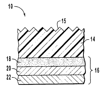
Referring to the drawings, wherein like structures are provided with like
reference
designations, FigurelA depicts a security article 10 according to one
embodiment of the
CA 02599246 2010-04-06
Doc. No.: 18-32 CA/PCT DIV Patent
present invention. The security article 10 includes a light transmissive
substrate 14 formed with
an optical interference pattern 15 on an outer first surface thereof. A color
shifting optical
coating 16 is formed on an opposing second surface of substrate 14 and is
discussed in further
detail below. The combination of substrate 14 and color shifting optical
coating 16 forming
5 security article 10 provide a security feature that reduces the possibility
of duplication, forgery
and/or counterfeiting of an object having security article 10 thereon.
The optical interference pattern 15 formed on the outer surface of light
transmissive
substrate 14 can take various conventional forms including diffraction
patterns such as
diffraction gratings, refraction patterns, holographic patterns such as two
dimensional and three-
dimensional holographic images, corner cube reflectors, or other like
interference patterns. The
particular methods and structures that form optical interference pattern 15
are known by those
skilled in the art. For example, embossing the light transmissive substrate to
form an interference
pattern thereon can be done by well known methods, such as embossing the
surface of a plastic
film by pressing it in contact with a heated nickel embossing shim at high
pressure. Other
methods include photolithography, molding of the plastic film against a
patterned surface, and
the like.
Generally, moldable materials are used to form light transmissive substrate 14
and
include, for example, plastics such as polyethylene terephthalate (PET),
especially PET type G,
polycarbonate, acrylics such as polyacrylates including polymethyl
methacrylate (PMMA),
polyacrylonitrile, polyvinyl chloride, polystyrene, polypropylene,
polynaphthalene terephthalate
(PNT), mixtures or copolymers thereof, and the like. It is preferred that
light transmissive
substrate 14 be substantially composed of a transparent material such as
polycarbonate. The
substrate 14 is formed to have a suitable thickness of about 5 micrometres to
about 100
micrometres, and preferably a thickness of about 12 micrometres to about 25
micrometres. In
addition, substrate 14 can be made of one layer or multiple layers of
substrate materials.
In one embodiment, substrate 14 can be produced from a thermoplastic film that
has been
embossed by heat softening the surface of the film and then passing the film
through embossing
rollers which impart the diffraction grating or holographic image onto the
softened surface. In
this way, sheets of effectively unlimited length can be formed with the
diffraction grating or
holographic image thereon.
As shown in Figure IA, the color shifting optical coating 16 is a multilayer
optical
interference film that includes an absorber layer 18, a dielectric layer 20,
and a reflector layer 22.
The absorber layer 18 is deposited on light transmissive substrate 14 by a
conventional
CA 02599246 2007-09-12
Doc. No.: 18-32 CA/PCT DIV Patent
6
deposition process such as physical vapor deposition (PVD), sputtering, or the
like. The
absorber layer 18 is formed to have a suitable thickness of about 30-150
Angstroms(A), and
preferably a thickness of about 50-100 A. The absorber layer 18 can be
composed of a semi-
opaque material such as a grey metal, including metals such as chromium,
nickel, titanium,
vanadium, cobalt, and palladium, as well as other metals such as iron,
tungsten, molybdenum,
niobium, aluminum, and the like. Various combinations and alloys of the above
metals may
also be utilized, such as Inconel (Ni-Cr-Fe). Other absorber materials may
also be employed in
absorber layer 18 including metal compounds such as metal fluorides, metal
oxides, metal
sulfides, metal nitrides, metal carbides, metal phosphides, metal selenides,
metal silicides, and
combinations thereof, as well as carbon, germanium, cermet, ferric oxide,
metals mixed in a
dielectric matrix, and the like.
The dielectric layer 20 is formed on absorber layer 18 by a conventional
deposition
process such as PVD, reactive DC sputtering, RF sputtering, or the like. The
dielectric layer 20
is formed to have an effective optical thickness for imparting color shifting
properties to
security article 10. The optical thickness is a well known optical parameter
defined as the
product rid, where , is the refractive index of the layer and d is the
physical thickness of the
layer. Typically, the optical thickness of a layer is expressed in terms of a
quarter wave optical
thickness (QWOT) that is equal to4 rid/1, where A is the wavelength at which a
QWOT
condition occurs. The optical thickness of dielectric layer 20 can range from
about 2 QWOT at
a design wavelength of about 400 nm to about 9 QWOT at a design wavelength of
about
700nm, and preferably 2-6 QWOT at 400-700 nm, depending upon the color shift
desired.
Suitable materials for dielectric layer 20 include those having a"high"index
of refraction,
defined herein as greater than about 1.65, as well as those have a "low" index
of refraction,
which is defined herein as about 1.65 or less.
Examples of suitable high refractive index materials for dielectric layer 20
include zinc
sulfide (ZnS), zinc oxide (ZnO), zirconium oxide (ZrO2), titanium dioxide
(TiO2), carbon (C),
indium oxide (In2O3), indium-tin-oxide (ITO), tantalum pentoxide (Ta2O5),
ceric oxide
(CeO2), yttrium oxide (Y203), europium oxide (Eu2O3), iron oxides such as
(II)diiron(III)
oxide (Fe304) and ferric oxide (Fe2O3), hafnium nitride (HfN), hafnium carbide
(HfC),
hafnium oxide (Hf02), lanthanum oxide (La2O3), magnesium oxide (MgO),
neodymium oxide
(Nd2O3), praseodymium oxide (Pr6011), samarium oxide (Sm2O3), antimony
trioxide (Sb2O3),
silicon carbide (SiC), silicon nitride (Si3N4), silicon monoxide (SiO),
selenium trioxide
(Se2O3), tin oxide (Sn02), tungsten trioxide (W03), combinations thereof, and
the like.
CA 02599246 2007-09-12
Doc. No.: 18-32 CA/PCT DIV Patent
7
Suitable low refractive index materials for dielectric layer 20 include
silicon dioxide
(SiO2), aluminum oxide (A1203), metal fluorides such as magnesium fluoride
(MgF2),
aluminum fluoride (A1F3), cerium fluoride (CeF3), lanthanum fluoride (LaF3),
sodium
aluminum fluorides (e. g., Na3A1F6 orNa5Al3F14), neodymium fluoride (NdF3),
samarium
fluoride (SmF3), barium fluoride (BaF2), calcium fluoride (CaF2), lithium
fluoride (LiF),
combinations thereof, or any other low index material having an index of
refraction of about
1.65 or less. For example, organic monomers and polymers can be utilized as
low index
materials, including dienes or alkenes such as acrylates (e. g.,
methacrylate), perfluoroalkenes,
polytetrafluoroethylene (Teflon), fluorinated ethylene propylene (FEP),
combinations thereof,
and the like.
The reflector layer 22 is formed on dielectric layer 20 by a conventional
deposition
process such as PVD, sputtering, or the like. The reflector layer 22 is formed
to have a suitable
thickness of about 300-1000A, and preferably a thickness of about 500-1000 A.
The reflector
layer 22 is preferably composed of an opaque, highly reflective metal such as
aluminum,
silver, copper, gold, platinum, niobium, tin, combinations and alloys thereof,
and the like,
depending on the color effects desired. It should be appreciated that semi-
opaque metals such
as grey metals become opaque at approximately 350-400 A. Thus, metals such as
chromium,
nickel, titanium, vanadium, cobalt, and palladium, or cobalt-nickel alloys
(which would be
magnetic), could also be used at an appropriate thickness for reflector layer
22.
In addition, reflector layer 22 can be composed of a magnetic material such as
a cobalt-
nickel alloy, or can be formed of a semitransparent material, to provide for
machine
readability for security verification. For example, machine readable
information may be placed
on a backing underlying the optical coating, such as personal identification
numbers (PINS),
account information, business identification of source, warranty information,
or the like. In an
alternative embodiment, reflector layer 22 can be segmented to allow for
partial viewing of
underlying information either visually or through the use of various optical,
electronic,
magnetic, or other detector devices. This allows for detection of information
below optical
coating 16, except in those locations where reflector segments are located,
thereby enhancing
the difficulty in producing counterfeits. Additionally, since the reflector
layer is segmented in
a controlled manner, the specific information prevented from being read is
controlled,
providing enhanced protection from forgery or alteration.
By using an absorber/dielectric/reflector design for color shifting optical
coating 16,
such as shown in Figure IA, high chroma variable color effects are achieved
that are
CA 02599246 2007-09-12
Doc. No.: 18-32 CA/PCT DIV Patent
8
noticeable to the human eye. Thus, an object having security article 10
applied thereto will
change color depending upon variations in the viewing angle or the angle of
the object relative
to the viewing eye. As a result, the variation in colors with viewing angle
increases the
difficulty to forge or counterfeit security article 10. By way of example, the
color-shifts that
can be achieved utilizing color shifting optical coating 16 in accordance with
the present
invention include, but are not limited to, gold-to-green, green-to-magenta,
blue-to-red, green-
to-silver, magenta-to-silver, magenta-to-gold, etc.
The color shifting properties of optical coating 16 can be controlled through
proper
design of the layers thereof. Desired effects can be achieved through the
variation of
parameters such as thickness of the layers and the index of refraction of each
layer. The
changes in perceived color which occur for different viewing angles or angles
of incident light
are a result of a combination of selective absorption of the materials
comprising the layers and
wavelength dependent interference effects. The interference effects, which
arise from the
superposition of the light waves that have undergone multiple reflections and
transmissions
within the multilayered structure, are responsible for the shifts in perceived
color with
different angles.
Figure 113 depicts a security article 30 according to an alternative
embodiment of the
present invention. The security article 30 includes elements similar to those
discussed above
with respect to security article 10, including a light transmissive substrate
14 formed with an
optical interference pattern on a surface thereof, and a color shifting
optical coating 16 that is a
multilayer film. The optical coating 16 is formed, however, on the same side
as the
interference pattern on substrate 14 by conventional deposition processes. The
optical coating
16 includes an absorber layer 18 on the interference pattern, a dielectric
layer 20 on absorber
layer 18, and a reflector layer 22 on dielectric layer 20. As shown in
FigurelB, each of these
layers formed on substrate 14 conforms to the shape of the interference
pattern such as a
holographic image.
Figure 2A depicts a security article 40 according to another embodiment of the
present
invention. The security article 40 includes elements similar to those
discussed above with
respect to security article 10, including a light transmissive substrate 14
formed with an optical
interference pattern 15 on an outer first surface thereof, and a color
shifting optical coating 16
formed on an opposing second surface of substrate 14. The optical coating 16
is a multilayer
film that includes an absorber layer 18 and a dielectric layer 20 thereon, but
does not include
the reflector layer. This allows optical coating 16 to be transparent to light
incident upon the
CA 02599246 2007-09-12
Doc. No.: 18-32 CA/PCT DIV Patent
9
surface thereof, thereby providing for visual verification or machine
readability of information
below optical coating 16 on a carrier substrate (not shown).
Figure 2B depicts a security article 50 according to an alternative embodiment
of the
present invention. The security article 50 includes elements similar to those
discussed above
with respect to security article 40, including a light transmissive substrate
14 formed with an
optical interference pattern on a surface thereof, and a color shifting
optical coating 16 that is a
multilayer film. The optical coating 16 is formed, however, on the same side
as the
interference pattern on substrate 14 by conventional deposition processes. The
optical coating
16 includes an absorber layer 18 on the interference pattern, and a dielectric
layer 20 on
absorber layer 18. This allows optical coating 16 to be transparent to light
incident upon the
surface thereof, providing for visual verification or machine readability of
information on a
carrier substrate.
Figure 3 depicts a security article 60 according to a further embodiment of
the present
invention. The security article 60 includes elements similar to those
discussed above with
respect to security article 10, including a light transmissive substrate 14
formed with an optical
interference pattern 15 on an outer first surface thereof, and a color
shifting optical coating 26
applied to an opposing second surface of substrate 14. The color shifting
optical coating 26 is
formed from a layer of color shifting ink or paint that includes a polymeric
medium
interspersed with a plurality of optical interference flakes having color
shifting properties.
The color shifting flakes of optical coating 26 are formed from a multilayer
thin film
structure that includes the same basic layers as described above for the
optical coating 16 of
security article 10. These include an absorber layer, a dielectric layer, and
optionally a
reflector layer, all of which can be composed of the same materials discussed
above in relation
to the layers of optical coating 16. The flakes can be formed to have a
symmetrical multilayer
thin film structure, such as
absorber/dielectric/reflector/dielectric/absorber, or
absorber/dielectric/absorber. Alternatively, the flakes can have a
nonsymmetrical structure,
such as absorber/dielectric/reflector. The flakes are formed so that a
dimension on any surface
thereof ranges from about 2 to about 200 microns.
Typically, the multilayer thin film structure is formed on a flexible web
material with a
release layer thereon. The various layers are deposited on the web by methods
well known in
the art of forming thin coating structures, such as PVD, sputtering, or the
like. The multilayer
thin film structure is then removed from the web material as thin film flakes,
which can be
added to a polymeric medium such as various pigment vehicles for use as an ink
or paint. In
CA 02599246 2010-04-06
Doc. No.: 18-32 CA/PCT DIV 10 Patent
addition to the flakes, additives can be added to the inks or paints to obtain
desired color
shifting results. These additives include lamellar pigments such as aluminum
flakes, graphite,
mica flakes, and the like, as well as non-lamellar pigments such as aluminum
powder, carbon
black, and other colorants such as organic and inorganic pigments, and colored
dyes.
Suitable embodiments of the flake structure are disclosed in U.S. Patent No.
6,157,489.
Other suitable embodiments of color shifting or optically variable flakes
which can be used in
paints or inks for application in the present invention are described in U. S.
Patent Nos.
5,135,812, 5,171,363, 5,278,590, 5,084,351, 4,838,648, and 4,168,983.
For example, U. S. Patent. 5,135,812 discloses a symmetrical optical
multilayer film
which is composed either of transparent all-dielectric stacks, or transparent
dielectric and semi-
transparent metallic layered stacks. In the case of an all-dielectric stack,
the optical coating is
made of alternating layers of high and low index of refraction materials. In
U. S. Patent No.
5,278,590 to Phillips et al., a symmetrical three-layer optical interference
coating which can be
formed into flakes is disclosed and includes first and second partially
transmitting absorber
layers that have essentially the same composition and thickness, with a
dielectric spacer layer
located between the first and second absorber layers. The dielectric layer is
composed of a
material having a low index of refraction such as magnesium fluoride.
The color shifting ink or paint utilized to form optical coating 26 on
security device 60
can be applied by conventional coating devices and methods known to those
skilled in the art.
These include, for example, various printing methods such as silk screen,
intaglio, gravure or
flexographic methods, and the like. Alternatively, optical coating 26 can be
formed on security
device 60 by coextruding a polymeric material containing color shifting
flakes, with the plastic
material used to form substrate 14 having interference pattern 15.
Figure 4 depicts a security article 70 according to another embodiment of the
present
invention. The security article 70 includes a light transmissive substrate 14
formed with an
optical interference pattern 15 on an outer surface thereof. A color shifting
pigment is dispersed
within substrate 14 and comprises a plurality of multilayer optical
interference flakes, such as
material that forms substrate 14 prior to formation thereof. Preferably, the
flakes are oriented so
those described above with respect to security article 40. The flakes are
dispersed within the that
they lie parallel to the planar back surface of substrate 14 opposite
CA 02599246 2007-09-12
Doc. No.: 18-32 CA/PCT DIV Patent
11
from the outer surface thereof in order to provide maximum color shifting
effects. The various
security articles as described above can be used in a variety of applications
to provide for
enhanced security measures such as anticounterfeiting. The security articles
can be utilized in
the form of a label, tag, ribbon, security thread, tape, and the like, for
application in a variety
of objects such as security documents, monetary currency, credit cards,
merchandise
packaging, license cards, negotiable notes, bank bonds, paper, plastic, or
glass products, or
other similar objects.
The security articles of the invention can be transferred and attached to
various objects
by a variety of conventional processes. For example, the security articles can
applied to an
object by use of a release layer. Figure 5 shows security article 10 with a
release layer 62
formed on substrate 14. The release layer 62 is of a suitable type to allow
security article 10 to
be removed therefrom during the application process, such as by a hot-
stamping process. The
release layer 62 may be a polymeric material such as polyvinyl chloride,
polystyrene,
chlorinated rubber, acrylonitrile-butadiene- styrene copolymer,
nitrocellulose, methyl
methacrylate, acrylic copolymers, fatty acids, waxes, gums, gels, and mixtures
thereof. The
release layer is coupled to a carrier structure 64, which can be part of
various manufacturing
belts or other processing structures that assist in transferring security
article 10 to the final
structural element.
As shown in Figure 6, the release layer is removed when security article 10
has been
applied to an object such as by hot-stamping, and the security article is
coupled to a carrier
substrate 66 by way of an adhesive layer 68. The carrier substrate 66 may take
the form of the
final structural object to which security article 10 is to be bonded, such as
those objects
discussed above. The materials forming carrier substrate 66 can be selected
from plastics,
cellulose, composites, polyester films, PET sheets, mylar sheets, cellophane,
polypropylene,
paper, rag/cotton, combinations thereof, and the like. The material of
adhesive layer 68 can be
selected from acrylic-based polymers, UV activated adhesives, ethylene vinyl
acetate,
polyarnides, and the like.
Figures 7-8 depict the method and final structure of affixing a security
article, such as
security article 30, to a carrier substrate 66 through a hot-stamping process.
Figure 7 shows
security article 30 with a release layer 62 formed on one side of a light
transmissive substrate
24, such as an acrylic coating with an interference pattern formed thereon.
The substrate 24
may be composed of other materials such as those discussed above relative to
substrate 14,
including polystyrene, polvacrylonitrile, polyvinyl chloride, and the like.
CA 02599246 2007-09-12
Doe. No.: 18-32 CA/PCT DIV Patent
12
The release layer 62 is formed on the side opposite from optical coating 16 on
the
interference pattern, and is attached to a carrier structure 64. The release
layer 62 allows
security article 30, including substrate 24, absorber layer 18, dielectric
layer 20, and reflector
layer 22, to be released from carrier structure 64 during the hot-stamping
process. Generally,
carrier structure 64 can be composed of various materials with various
thicknesses which are
known by those skilled in the art. For example, when carrier structure 64 is
formed of PET, the
thickness preferably ranges from about 10, urn to about75, um. Other materials
and thickness
ranges are applicable in light of the teachings contained herein. Furthermore,
the thickness of
light transmissive substrate 24, when taking the form of an acrylic material,
can range from
about 3um to about 20, urn with an embossed surface. Generally, substrate 24
should have a
lower melting point or glass transition temperature than the optical coating,
while being
transparent.
Prior to hot-stamping, an adhesive layer 68 is formed on reflector layer 22,
with the
adhesive layer having a thickness of about2 Fm to about 20,um. As shown in
Figure 8, the
release layer and carrier structure are removed when security article 30 has
been applied to an
object such as a carrier substrate 66 by hot-stamping, with security article
30 being coupled to
carrier substrate 66 by way of adhesive layer 68. The bonding of adhesive
layer 68 against
carrier substrate 66 occurs as a heated metal stamp (not shown) comes into
contact with carrier
structure 64. The heated metal stamp simultaneously forces adhesive layer 68
against carrier
substrate 66 while heating adhesive layer 68 to more effectively bond to
carrier substrate 66.
Furthermore, the heated metal stamp softens release layer 62 thereby aiding in
releasing
security article 30 from carrier structure 64 which is subsequently discarded.
Once security
article 30 has been attached to carrier substrate 66, the image produced by
security article 30 is
viewed from substrate 24 toward optical coating 16.
The following examples are given to illustrate the present invention, and are
not
intended to limit the scope of the invention.
Example 1
Optical coatings composed of color shifting flakes in a polymeric vehicle were
formed
by a drawdown process on light transmissive substrates composed of PET films
containing a
holographic image. The drawdown vehicle included two parts lacquer/catalyst
and one part
color shifting flakes. The color shifting flakes utilized had color shifting
properties of green-
to-magenta, blue-to-red, and magenta-to-gold.
CA 02599246 2007-09-12
Doc. No.: 18-32 CA/PCT DIV Patent
13
Example 2
A color shifting optical coating having a three-layer design was formed on an
embossed transparent film to produce a security article. The optical coating
was formed on the
flat surface of the transparent film on the side opposite from the embossed
surface. The optical
coating was formed by depositing an absorber layer composed of chromium on the
flat surface
of the transparent film, depositing a dielectric layer composed of magnesium
fluoride on the
absorber layer, and depositing a reflector layer of aluminum on the dielectric
layer.
Alternatively, the aluminum layer can be deposited so that it is transparent.
This would
allow printed information on an object to be read underneath the optical
coating. Further, the
reflector layer can alternatively be composed of a magnetic material. Such a
magnetic feature
in the color shifting component when added to the holographic component would
give three
independent security features to the security article.
The embossed film and optical coating forming the security article can be
rigidly
affixed to a carrier substrate, or can be attached to a release layer so that
the security article
can be hot stamped to a surface of an object. In addition, the hot stamped
image of the color
shifting thin film can be in the form of a pattern, as for example, dots,
lines, logos, or other
images. This pattern of optically variable effects will add an even greater
degree of deterrence
to counterfeiting.
The present invention may be embodied in other specific forms without
departing from
its spirit or essential characteristics. The described embodiments are to be
considered in all
respects only as illustrative and not restrictive. The scope of the invention
is, therefore,
indicated by the appended claims rather than by the forgoing description. All
changes which
come within the meaning and range of equivalency of the claims are to be
embraced within
their scope.
What is claimed is:
CA 02599246 2007-09-12
Doc. No.: 18-32 CA/PCT DIV Patent
14
1. A security article comprising:
a light transmissive substrate having a first surface and an opposing second
surface, the first
surface having an optical interference pattern; and
a color shifting optical coating on the first or second surface of the
substrate, the optical
coating providing an observable color shift as the angle of incident light or
viewing angle
changes;
wherein a segmented layer allows partial viewing of some regions while
obscuring viewing of
other regions.
2. The security article of claim 1 wherein the substrate is composed of a
plastic material.
3. The security article of claim 2, wherein the plastic material is selected
from the group
consisting of polyethylene terephthalate, polycarbonate, polyvinyl chloride,
polyacrylates,
polyacrylonitrile, polystyrene, polypropylene, polynaphthalene terephthalate,
and mixtures or
copolymers thereof.
4. The security article of claim 1, wherein the optical interference pattern
is a diffraction
grating pattern or a holographic image pattern.
5. The security article of claim 1, wherein the color shifting optical coating
is a multilayer
optical interference film including an absorber layer on first or second
surface of the substrate,
and a dielectric layer on the absorber layer.
6. The security article of claim 1, wherein the color shifting optical coating
is a multilayer
optical interference film including an absorber layer on the first or second
surface of the
substrate, a dielectric layer on the absorber layer, and a reflector layer on
the dielectric layer.
7. The security article of claim 1, wherein the color shifting optical coating
is a multilayer
optical interference film including an absorber layer, a dielectric layer, and
a reflector layer;
and wherein the reflector layer is the segmented layer.
8. The security article of claim 1, further comprising a release layer on the
substrate.
CA 02599246 2007-09-12
Doe. No.: 18-32 CA/PCT DIV Patent
9. A security article as claimed in claim 1
wherein the interference pattern includes a diffraction grating pattern or a
holographic image
pattern wherein the colour shifting optical coating includes a color shifting
multilayer optical
film comprising:
5 an absorber layer on the first or second surface of the substrate;
a dielectric layer on the absorber layer; and
a reflector layer on the dielectric layer; and,
wherein the optical film coating provides an observable color shift as the
angle of incident
light or viewing angle changes.
10. A security article as defined in claim 9, wherein the reflector layer is a
segmented layer.
11. A security article as defined in claim 1 wherein the color shifting
coating is on the second
surface of the substrate and wherein the segmented layer is a reflector layer.
12. A security article as defined in claim 1 wherein the color shifting
coating is on the first
surface of the substrate and wherein the segmented layer is a reflector layer.
13. A security article comprising: a light transmissive substrate having a
first surface and an
opposing second surface, said first surface having a diffraction grating
pattern or a holographic
image pattern formed thereon; and a color-shifting multilayer optical film
structure formed on
said diffraction grating pattern or said holographic image pattern formed on
said first surface
of said light transmissive substrate, so as to conform to the shape thereof,
said color-shifting
multilayer optical film structure being defined by an optical absorber layer
formed directly on
said diffraction grating pattern or said holographic image pattern formed on
said first surface
of said light transmissive substrate, a dielectric layer formed directly on
said optical absorber
layer, and a reflector layer formed directly on said dielectric layer said
reflector layer
replicating said diffraction pattern or said holographic image pattern formed
on said first
surface of said light transmissive substrate; wherein said color-shifting
multilayer optical film
structure provides color shifting with change of viewing angle or angle of
incident light; and
wherein the reflector layer is segmented forming a layer having blocking
opaque regions and
non-blocking windowed regions.
CA 02599246 2007-09-12
Doc. No.: 18-32 CA/PCT DIV Patent
16
14. A security article as defined in claim 13, wherein the non-blocking
windowed regions
provide no color shifting with a change of viewing angle or incident light.