Note: Descriptions are shown in the official language in which they were submitted.
CA 02599319 2007-08-24
WO 2006/094164 PCT/US2006/007528
OPTICAL TRANSMISSION SYSTEM INCLUDING
DISPERSION SLOPE COMPENSATION
Cross-Reference to Related Applications
The present application clainis the benefit of the filing date of U.S.
Provisional
Application Ser. No. 60/657,125, filed February 28, 2006, the teachings of
wliich are
fully incorporated herein by reference.
Field
The invention relates to the optical transniission of infoimation and more
particularly, to an optical transmission system including dispersion slope
compensation.
Back rg ound
The availability of high performance optical amplifiers such as the Erbium-
Doped
Fiber-Amplifier (EDFA) has facilitated continued development of wavelength
division
multiplexing (WDM) for optical transmission systems. In a WDM transniission
system,
two or more optical data carrying channels are combined onto a common path for
transmission to a remote receiver. In a long-haul optical fiber system, the
set of
wavelengtli chaimels may be amplified simultaneously in an optical amplifier
based
repeater. The EDFA is particularly useful in this application because of its
ability to
amplify multiple wavelength channels with little or no crosstalk penalty.
In general, it is advantageous to operate long-haul transmission systems at a
high
data rate per channel. Long-haul systems niay operate, for example at
Synch.ronous
Digital Hierarchy (SDH) standards up to 40 Gb/s or more. As the bit rates rise
through
the gigabit per second range, there is the need for an increase in the optical
powers
launched into the transmission fiber, e.g. to 1 mW per channel or more. As
demonstrated by Cai et al. ("RZ-DPSK field trial over 13 100 km of installed
non-slope-
matched submarine fibers", Journal of Lightwave Technology in Vol. 23, No. 1,
January
2005 pp. 95-103), variants of the return-to-zero (RZ) modulation foimat are
particularly
useful for transmitting large amounts of data over optically anzplified fiber
patlis.
For long distance operation at higher data rates (e.g., 40 Gb/s RZ-DPSh
channels), however, there is a need to control chromatic dispersion and the
dispersion
slope to ensure low dispersion penalties. Dispersion shifted optical fibers
have been the
preferred transmission medium where there is a need to control chromatic
dispersion.
CA 02599319 2007-08-24
WO 2006/094164 PCT/US2006/007528
The combination of long 'distance transmission, low dispersion and high
channel power
may result in crosstalk, or mixing of channels through the sliglit
nonlinearity in the
transmission fiber. The transmission of many WDM channels over transoceanic
distances can be limited by the nonlinear interactions between chamiels, which
in turn is
affected by the amount of dispersion. This subject was reviewed by Tkach et
al. (Journal
of Lightwave Technology in Vol. 13, No. 5, May 1995 pp. 841-849).
One solution to the problem of nonlinear interactions between chaiuiels is
known
as "dispersion mapping" where the generation of mixing products is reduced by
offsetting the zero dispersion wavelength in the transmission fiber from the
operating
wavelengths of the transmitter. In this established technique, several
amplifier sections
may have dispersion shifted fiber spans with either positive or negative
dispersion. The
dispersion accumulates over many amplifier spans, for example, for distances
of 500.to
1000 kn1, and the accumulated dispersion is followed by fiber with the
opposite
dispersion to bring the average dispersion (as averaged over the length of the
cable) back
to zero. One problem with this scheme is that conventional dispersion maps
only
compensate for the dispersion of the transmission fiber over a limited
bandwidth (or a
sub-set of WDM chamiels) while allowing the dispersion to accumulate to large
values,
for the majority of WDM chaimels. To lnitigate this problem, additional
dispersion
compensation using dispersion compensating fibers at the terminals (e.g., the
transmitter
and/or receiver) may be applied either before the channels are multiplexed at
the
transmitter, or after the channels are demuliplexed at the receiver. However,
this method
of dispersion compensation generally does not coinpensate for accumulation of
dispersion slope within the optical bandwidth of a data channel.
Using these conventional dispersion management schemes, the long-haul
transmission of 40 Gb/s channels suffers from dispersion-slope penalty. High
speed
optical data channels may require high chamiel power for good optical signal
to noise
ratio (SNR). As is well known, long optical transmission systems that suffer
from
optical fiber nonlinearities work better with a narrow pulse transmissiom
forniat, such as
RZ, CRZ, and RZ-DPSK. Unfortunately, narrow optical pulses have a wide optical
spectrum. Dispersion slope causes the dispersion to change over the bandwidth
of the
signal having spectrally-broad pulses, which causes signal distortion and
limits the ability
to increase the bit rate per channel of such systems,
2
CA 02599319 2007-08-24
WO 2006/094164 PCT/US2006/007528
One method of improving 40 Gb/s operation is 'to use transmission fibers known
as "dispersion-flattened" fibers. Unfortunately, the vast majority of existing
systems that
were designed to work at lower bit rates use conventional fiber that has high
accumulated
dispersion slope. Thus, there is a need for systems and methods to improve the
performance of high-speed signals, for example, when used witll conventional
dispersion
maps.
Brief Description of the Drawing
Features and advantages of embodiments of the claimed subject matter will
become apparent as the following Detailed Description proceeds, and upon
reference to
the Drawings, where like numerals depict like parts, and in which:
Fig. 1 shows a simplified block diagram of a segnient of an exemplary optical
transmission path usefiil in connection with the present invention;
Fig. la shows a plot of accumulated cluomatic dispersion associated with
optical
transmission path segment illustrated in Fig. 1;
Fig. 2 shows a plot of the chromatic dispersion vs. wavelength over the entire
length of an optical transmission system;
Fig. 3 shows a plot of the group delay vs. wavelength for a system as shown in
Fig. 1, along with the optical spectlum of the transmitted signal;
Fig. 4 shows a simplified block diagram of one exemplary embodiment of a
WDM transmission system, consistent with the present invention, which has a
dispersion
slope compensator located in each chamiel path;
Fig. 5 shows a simplified block diagram of oiie embodiment of a transmitter
that
can be used in combination with the dispersion slope-compensated system,
consistent
witli the present invention;
Fig. 5a shows exemplaiy waveforms output from an exemplary transmitter
consistent with the invention using a DPSK modulation format and different
levels of
amplitude modulation;
Fig. 6 shows a plot of transmission perfoimance vs. pulse width for a 6,250 km
transmission path;
Fig. 7 shows a plot of transmission performance vs. average channel power for
a
6,250 km transmission path; and
3
CA 02599319 2007-08-24
WO 2006/094164 PCT/US2006/007528
Fig. S shows a simplified block diagram of one embodiment of an apparatus that
can compensate for both dispersion and dispersion slope.
4
CA 02599319 2007-08-24
WO 2006/094164 PCT/US2006/007528
Detailed Description
For simplicity and ease of explanation, various exemplary embodiments will be
described herein. It is to be understood, however, that 'the embodiments
described herein
are presented by way of illustration, not of limitation.
Fig. 1 shows an example of a 500 km segment of an optical transmission path
including optical amplifiers 110N concatenated with sections of dispersion
fiber 111, 112
so that the end-to-end accumulated dispersion is relatively small, while
maintaining a
large local dispersion. For a high perfonnance long haul system, it is
desirable to have
large local dispersion (e.g., to reduce nonlinear mixing) and low end-to-end
dispersion
(e.g., for high signal fidelity). These two characteristics may be satisfied
by using a
"dispersion managed" amplifier cable (also known as a "dispersion map"). One
example
of a dispersion map is a non-zero dispersion shifted fiber (N2-DSF) dispersion
map. In a
dispersion managed cable, two different types of fiber may be used with
opposite signs of
dispersion. In this example, the negative dispersion fibers 111N have a mean
dispersion
of -2 ps/l:ni-mn and the positive dispersion fibers 112 have a mean dispersion
of
+17 ps/km-iun. The lengths of the two fiber types may be selected to be in
proportion to
the ratio of dispersion values.
The accumulated dispersions for three exemplary channels are shown in Fig. 1 a
as cuives 101, 102, and 103. For this arrangement, the chromatic dispersion
first
accumulates negative dispersion, then positive dispersion, and eventually
returns to zero
at the end of the dispersion period. In some types of fibers, the
characteristic of
returning to zero (for accumulated dispersion) for curve 101 is only true for
the channel
located at the mean zero dispersion wavelength. The curve 102 shows that a
higher
wavelength channel may accumulate a net positive dispersion as indicated by
104 and the
curve 103 shows that a lower wavelength chaimel may accumulate a net negative
dispersion as indicated by 105.
This characteristic, known as dispersion slope, is illustrated in plot of
dispersion
vs. wavelength for each fiber type shown in Fig. 2. Curve 201 shows the
dispersion vs.
wavelength for the negative dispersion fibers 111N, curve 202 shows the
dispersion vs.
wavelength for the positive dispersion fibers 112, and cuive 203 shows the
dispersion vs,
wavelength characteristic for the entire span. Even for the point at which the
accumulated dispersion is zero (indicated as a,o in the figure) for curve 203,
there is still a
large dispersion slope, which is a consequence of both fiber types having a
positive
5
CA 02599319 2007-08-24
WO 2006/094164 PCT/US2006/007528
dispersion slope. This linear change in dispersion may be approximated by the
equation
D = SL(AS;g - Ao) (1)
where Xs;g is the signal wavelength (the independent variable in the Fig. 2),
a,o is the
fiber's zero dispersion wavelengtli, S is the dispersion slope of the fiber
typically stated
in units of ps/lan-nm2, and L is the fiber's length. Given this linear
approxiniation to the
fiber's dispersion, the change in group delay (Ati) as a function of
wavelength niay be
approximated by equation (2), which gives the well-known parabolic shape:
~ig - 2 u ) z (2)
L~ Z =(,a.s
In Fig. 3, group delay curve 301 represents equation (2) calculated for a
6,250 kin
span of transmission fiber with a dispersion map similar to Fig. 1. The values
used in the
equation to produce the curve 301 are S=0.075ps/krn-nm2 , L=6,250km, and ~,o =
1550nm. Cui-ve 302 represents an optical spectrum for a 43Gb/s optical RZ
optical
signal, for a can-ier to side-band ratio of OdB, where the pulse width is
about 6.7 psec.
The exemplary curves 301, 302 show that the group delay changes by a large
fraction of
the bit period over the optical spectnim of the data signal. The bit time of
the 43GB/s
data signal is about 23.3psec. Thus, a data signal having a spectium
represented by curve
302 would suffer large penalty if transmitted through that aniount of
dispersion slope.
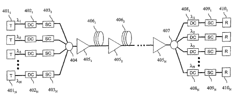
Fig. 4 shows a simplified block diagram of an exemplary WDM optical
transmission system, consistent with one embodiment of the invention. As
shown, the
optical transmission system includes a plurality of transmitters 4011-401N for
generating
WDM optical signals at associated channels to be transmitted over an optical
path to
remote receivers. The transmitters 401 1-401N can be of several known types in
the art
including, for example, RZ, CRZ, and/or RZ-DPSK transmitters. The 'output of
transmitters 4011-401N may be optically comiected to dispersion compensating
units or
dispersion compensators 4021-402N and then to dispersion slope compensating
units or
slope compensators 4031-403N. The expressions "optically connected" and
"optically
coupled" as used herein refer to any connection, coupling, link or the like by
which.
optical signals carried by one optical systein element are imparted to the
"connected" or
"coupled" element. Such "optically comiected" or "optically coupled" devices
are not
necessarily directly connected to one another and may be separated. by
interniediate
optical conzponents or devices. Likewise, the terms "connected" or "coupled"
as used
6
CA 02599319 2007-08-24
WO 2006/094164 PCT/US2006/007528
herein in regard to physical comiections or couplings is a relative term and
does not
require a direct physical connection.
The plurality of WDM channels may be multiplexed onto a common optical fiber
by coupler 404. The coupler 404 may be, for example, a simple NxN directional
coupler
or a wavelength router device. The plurality of WDM channels are then
transmitted over
the optical path including optical amplifiers 4051-405N and optical fiber
sections 4061-
406N. In the exemplary embodiment, this optical path may be similar in design
to that
shown in Fig. 1. Alternatively, the amplifier stages may be based on Raman
amplification and/or a combination of EDFA and Ranian amplifiers. The fiber
spans
used in this exemplary transmission system may be non-slope matched, as shown
in Fig.
1, or may include dispersion flattened fiber spans, or combinations of both
types.
At the receiver end, the optical transmission system may include a coupler 407
for de-multiplexing WDM channels onto separate paths. The receiver end of the
optical
transmission system may also include a plurality of dispersion compensators
4081-408N,
dispersion slope compensators 4091-409N and receivers 4101-410N. The receivers
4101-
410N may be balanced receivers such as the type known to those skilled in the
art. The
dispersion compensators 4081-40SN and the dispersion slope compensators 4091-
409N
may be implemented using techniques known to those skilled in the art, as
descrired in
greater detail below.
The illustrated exemplary embodiment of the optical transmission system shown
in Fig. 4 includes a combination of dispersion compensators 402 and 408 and
dispersion
slope compensators 403 and 409 located at both the transmit and receive
terminals. It
can be appreciated by those skilled in the art that it may be more cost
effective to locate
one type (or both types) of such compensators at only one end of the system.
For
example, another embodiment of the transmission system may include dispersion
coinpensators 4021-402N at the transmit end, dispersion compensators 40SI-408N
at the
receive end, and dispersion slope compensators 4091-409N at the receive end
only. Those
skilled in the art will also appreciate that the order of the dispersion
compensator and
dispersion slope compensator is interchangeable. .
In operation of the system, the amount of dispersion compensation in the
dispersion conlpensators 4021-402N and 4081-408N may be made to compensate
substantially for any accumulated dispersion through the system. In Fig. 1,
for example,
a high-wavelength channel accumulates an amount of dispersion indicated by 104
after
7
CA 02599319 2007-08-24
WO 2006/094164 PCT/US2006/007528
about 500km: Thus, after passing through about 6,000km (or 12 times the
500kni), the
high wavelength channel will accumulate a large aniount of dispersion to be
substantially
compensated by the dispersion compensators.
The amount of dispersion slope compensation in slope compensators 403 1-403N
and 4091-409N, may be made to compensate substantially for any accuniulated
dispersion
slope through the system. The group delay curve 301 in Fig. 3, for example,
shows how
the group delay changes with vvavelength corresponding to an accumulated
dispersion
slope of about 480 ps/nmz. The combination of slope compensators 4031-403N and
4091-
409N may be made to have a group delay characteristic that is substantially
equal in
magnitude to group delay curve 301, with opposite sign.
The illustrated exemplary embodiment includes the dispersion compensators and
dispersion slope compensators as two separate devices. As cari be appreciated
by those
of ordinary skill in the art, dispersion compensation and slope compensation
functions
may be combined into a common device, as described below and shown, for
example, in
Fig. S. ui one embodiment, a quadratically chiiped fiber grating may be
designed to
provide both the correct amount of dispersion compensation and dispersion
slope
compensation.
The illustrated exemplary embodiment includes a separate optical path for each
WDM optical chamiel. As can be appreciated by those skilled in the art,
chamiels may be
grouped into sub-bands that may be compensated in common devices. Also, the
number
of common dispersion compensating devices need not be equal to the number of
dispersion slope compensating devices. This is evident from looking at the
curves in Fig.
2, where it is observed that the amount of accumulated dispersion shown as
curve 203 is
substantially different over the wavelength range in interest. However, the
amount of
dispersion slope (i.e., the slope of cui-ve 203) is nearly the sanie for all
channels. Thus,
some channels may use a slope compensator but no dispersion compensator.
According to another embodiment of the transmission system, the dispersion
-slope compensators may also function as a fine-tuning element for the
dispersion
compensators, for example, by making the center wavelength of the dispersion
slope
compensator tunable. By tuning the center wavelength of the dispersion slope
compensator off of the center wavelength of the signal, one can obtain a
continuous
dispersion adjustment, which can be used to optimize the performance of the
WDM
chamiels. Adjusting. or tuning the center wavelength adjusts the, first order
dispersion,
8
CA 02599319 2007-08-24
WO 2006/094164 PCT/US2006/007528
while keeping the second-order dispersion fixed. The dispersion for a
dispersion slope
compensator may also be tuned, as stated above, as fine residual dispersion
tweaking to
match the liiik residual dispersion. The 40 Gb/s signals are very sensitive to
residual
dispersion, and the link dispersion could vary over time due to temperature
change.
Fig. 5 shows a simplified block diagram of one embodiment of a transinitter
that
may be used in the transmission system shown in Fig. 4. In the illustrated
exemplary
embodiment, laser 500 produces a CW light signal on path 501 that connects to
data
modulator 502. The data modulator 502 may modulate the optical signal to
impart
information thereto in a well-known fashion. A variety of data modulator
configurations
for applying a variety of modulation formats are well-l:nown to those of
ordinaiy skill in
the art. For example, the data modulator 502 may be configured. to modulate
the optical
signal using a well-known format such as NRZ, RZ, phase shift keying (PSK),
differential phase shift keying (DPSK), etc. The method is not limited,
however, to a
particular modulation format and other formats (e.g., OOK, DBPSK, DQPSK, etc.)
may
be used. Including the dispersion slope compensator into the optical
transmission system
may give greater flexibility to optimize the transmission format used in the
plurality of
transmitters.
In an embodiment wherein the data modulator 502 is configured to modulate the
optical signal to impart information thereto using a DPSK format, the data
modulator 502
may receive the data to be imparted to the optical signal 501 from a data
source 504 and,
modulate the optical signal 501 at a frequency determined by a clock 506 to
form a
DPSK modulated signal 503 in a well-known mamier. The DPSK modulated optical
inforniation signal 503 may be transmitted fi=om the data modulator 502 to an
amplitude
modulator 507, which places a synchronous intensity modulation on the optical
infoimation signal 503.
The intensity modulation imparted by the amplitude modulator 507 may be
periodic. To impart periodic amplitude modulation, the modulator 507 may be
driven by
a periodic signal, such as a sinusoidal or square wave signal. In one
embodiment, the
amplitude modulator 507 may be configured to impart amplitude modulation
without
also applying phase modulation to the signal. The amplitude modulator 507 may
thus
re-modulate the DPSK modulated signal 503 at a rate equal to the rate at which
data is
imparted to the optical signal 501 as defined by clock source 506 generating a
sinusoidal
signal. One example of intensity modulation imparted by an amplitude modulator
on a
9
CA 02599319 2007-08-24
WO 2006/094164 PCT/US2006/007528
DPSK modulated optical signal is described in greater detail in U.S. Patent
No.
6,556,326 and pending U.S. Patent Application Serial No. 10/780,830, which is
fully
incorporated herein by reference.
The DPSK data modulator 502 in such an embodiment may include a Mach-
Zehnder-type optical modulator as described, for example, in T. Chikama, et
al.,
"Modulation and Demodulation Tecluiiqucs in Optical Heterodyiie PSK
Transmission
Systems," Journal of Lightwave Technology, Vol. S, No. 3, March 1990 pages 309-
322,
the teachings of which are hereby incorporated by reference. In such a
configuration, the
optical phase of the DPSK modulated signal 503' emerging from the data
modulator
changes abruptly from 0 to 1 80 (or 0 to 7c radians) on the transitions
between
differential bits, thus providing a high-fidelity digital phase modulation.
In an embodiment where the data modulator 502 is a DPSK modulator, it may
also be advantageous to provide an electrical variable-delay 509 and an
amplitude
adjustnient 510. The variable delay 509 may be used to selectively adjust the
phase of
the amplitude modulation imparted by amplitude modulator 507 relative to the
phase of
the data modulation imparted by data modulator 502. The amplitude adjustment
510
may be used to set the depth of modulation that amplitude modulator 507
imparts on
signal 503. The optimal settings for these adjustments will depend on many
parameters
in the system, and can be determined empirically. In one embodiment, the delay
provided by variable delay 509 may be set to align the center of the data bits
on line 503
with the peak amplitude point of the synchronous amplitude modulation provided
by
amplitude modulator 507. Again, in a WDM system, the optimal setting for each
channel may not necessarily be the same and thus the channels may be
individually
optimized.
Using the combination of the exemplaiy transmitter shown in Fig. 5 in the
exemplary dispersion slope compensated WDM system shown in Fig. 4, it is
possible to
optimize the transmission perforniance by adjusting the pulse width of the
transmitter.
Fig. 5a also shows a series of waveforms 520-525, where each of the
illustrated
wavefonns results from a different level of depth of amplitude modulation
imparted by
the amplitude modulator 507. The progression of waveforms starting with 520
and.
going to 525 shows a progressively deeper aniplitude modulation and thus a
shorter pulse
width. Waveform 520 is an example of an intensity profile, for a conventional
DPSK
waveform, and is sometimes refenred to as representing Non-Return-to-Zero DPSK
CA 02599319 2007-08-24
WO 2006/094164 PCT/US2006/007528
(NRZ-DPSK). Waveforms 521, 522, 523, 524, and 525 illustrate amplitude
modulation
depths of 20%, 40%, 60%, 80%, and 100%, respectively. These different levels
of
amplitude modulation may, for exaniple, be established by the amplitude
adjustment
mechanism 510. The optical intensity of waveform 525 returns substantially to
zero
during contiguous blocks of binaiy 0's or n's and hence is sometimes referred
to as
representing Return-to-Zero DSPK (RZ-DPSK).
Fig. 6 shows the results of a transmission experiment perfornie.d over a
distance
of 6,250km using an amplifier chain similar to Fig. 1 and a 43GB/s RZ-DPSK
transmitter similar to Fig. 5. The figure shows the measured Q-factor vs. the
pulse width
(set at the transmitter) as a percentage of the bit time for the 43Gb/s pulse
for cases with
a dispersion slope compensator (cuive 601) and without a dispersion slope
compensator
(curve 602). In the illustrated exemplary embodiment, the pulse width is
adjusted
between about 25% and about 40% of the bit time associated with the,
transmitted signals
according to the description of Fig. 5.
The curves show a perfonnance advantage for pulse widths betv,reen about 25%
and about 40% when using a slope compensator at the receive terniinal. Also,
the curves
show that it is possible to operate the systems with a shorter pulse width
when using the
dispersion slope compensator. In particular, cuive 601 shows a maximum a Q-
factor of,
about 13.5dB for pulse widths between about 27-31% when slope compensation is
used,
whereas curve 602 shows a maximum Q-factor of about 11.5dB for pulse widths
between
about 31-33% when slope compensation is not used. Q factor is maximized at a
higher
value and at a shorter pulse width when slope compensation is used. In the
embodiment
illustrated in FIG. 6, for exanzple, at pulse widtlis below about 31 % the Q
factor of the
non-slope compensated system decreases and the Q factor of the slope
compensated
system increases. When upgrading an existing system, therefore, performaiice
can be
improved by compensating for dispersion slope and reducing the existing pulse
width, '
e.g. to a less than the optimum pulse width in the existing system without
slope-
compensation. Also, as shown, in a slope-compensated system at pulse widths
less than
about 40% Q-factor performance remains significantly improved compared to when
no
slope compensation is used with the same pulse width.
Fig. 7 show the results of a transmission experiment performed over the same
distance as in Fig. 6. One experimental transmission is made with a dispersion
slope
compensator and with the RZ-DPSK modulation fonnat and another experimental
11
CA 02599319 2007-08-24
WO 2006/094164 PCT/US2006/007528
transmission is made without a dispersion slope compensator and with the CSRZ-
DPSK
modulation fonnat. The figure shows the measured Q-factor vs. the average
optical
chaimel power expressed in dBm. Curve 701 was measured with the dispersiori
slope
compensation (RZ-DPSK) and curve 702 was measured without the slope
compensation
(CSRZ-DPSK). According to the experiment, the performance with the dispersion
slope
compensator is improved at eveiy power level and the addition of the
dispersion slope
compensator allows the WDM channel to operate at a higher optical power. Also,
the
ability to operate with narrow pulse widths having higher optical power gives
the channel
a better received signal-to-noise ratio and leads to improved perforniance.
Fig. 8 shows a simplified block diagram of one embodiment of a compensator
that can be used to compensate for both chromatic dispersion and dispersion
slope. In
operation, this apparatus may serve as both a dispersion compensator 408 and a
slope
compensator 409 in the receiver section and/or as a dispersion compensator 402
and
slope compensator 403 in the transmit section of the transmission system shown
in Fig.
4. An input optical signal enters the compensator apparatus on path 801 and
then gasses
into dispersion compensating fiber 802. One example of dispersion compensating
fiber
802 is an OFS Rightwave0 dispersion compensating module. Next, the signal
enters,
port 810 of an optical circulator 803. The signal emerges from circulator 803
on port 820
and then enters a fiber grating 804, such as a quadratically chirped fiber
grating. The
signal reflected off of grating 804 enters the circulator 803 back into port
820, and
emerges on port 830 of circulator 803 on path 806. In operation, dispersion
compensating fiber 802 may be designed to compensate the accumulated
dispersion in
the optical path including amplifiers 405 and fiber sections 406 '(see Fig.
4). The group
delay characteristic of a signal reflected off of grating 804 is designed to
compensate for
the dispersion slope of the optical path described above.
According to another alternative of the compensator shown in Fig. 8, the
dispersion compensating fiber 802 may be located between optical circulator
803 and
fiber grating 804. By doing this, the required length of dispersion
compensating fiber
802 can be shortened by half. According to a further embodiment of the
transmission
system, the slope compensator may also act as a channel selection filter,
similar to the
current 3-port channel dropping filter known to those skilled in the art.
A system, apparatus and method is thus provided for dispersion management that
yields improved transmission perforniance for WDM optical transmission
systems.
12 .
CA 02599319 2007-08-24
WO 2006/094164 PCT/US2006/007528
According to one aspect of the present invention, a dispersion slope-
compensating
element or slope compensator is used at the receive terminal and/or at the
transniit
terniinal to compensate for the accumulated dispersion-slope. This allows the
narrow
optical pulses (i.e., having wide optical bandwidth) to be used at higher
optical power
levels.
According to another aspect of the present invention, a WDM optical
transmission system includes a transmitter configured to provide a plurality
of optical
signals, each of the optical signals having associated data modulated thereon
and having
a naiYow pulse width (e.g. less than about 40%) of a bit time associated with
the data; a
receiver;,an optical fiber transmission path coupling the transmitter to the
receiver, the
transmissioii path establishing a end-to-end dispersion slope across a range
of
wavelengtlis transmitted from the transmitter to the receiver; and at least
one dispersion
slope compensator configured to compensate for at least a portion of the end-
to-end
dispersion slope, the at least one dispersion slope compensator being
positioned at the
transmitter or the receiver. The dispersion slope compensator may compensate
for slope
of at least one channel or block of channels. The slope compensator may also
act as a
channel selection filter. The optical path may include non-slope-matched
fibers and/or
dispersion flattened fibers.
According to another aspect of the present invention, a compensating apparatus
comprises an input path, a dispersion compensating fiber, an optical
circulator, a
compensatiiig element, and an output patli. The compensating element may be a
fiber
grating. Tlie dispersion compensating fiber may be located between the input
path and
the optical circulator or between the optical circulator and the compensating
element.
According to yet another aspect of the present invention, a WDM optical
transmission system includes a transmitter, a receiver, an optical fiber
transmission path
coupling the transmitter to the receiver, the transmission path establishing a
end-to-end
dispersion slope across a range of wavelengths transmitted, froni the
transmitter to the
receiver, and at least one dispersion slope compensator configured to
compensate for at
least a portion of the end-to-end dispersion slope, the at least one
dispersioii slope
compensator being positioned at the transinitter or the receiver. The
transmitter may be
configured to provide a plurality of optical signals, each of the optical
signals having
associated data modulated thereon using aDPSK modulation format and having a
periodic intensity modulation thereon at an intensity modulation depth equal
to about
13
CA 02599319 2007-08-24
WO 2006/094164 PCT/US2006/007528
100% to establish a pulse width less than about 31% of a bit time associated
with the
data. The transmitter may include an optical signal source configured to
generate at least
one of the optical signals; a data modulator coupled to the optical signal
source and
configured to modulate the data on the at least one of the optical signals at
a data
modulation fi=equency; and an amplitude modulator coupled to the optical
signal source
and configured to provide the periodic modulation of the intensity of the at
least one of
the optical signals. Using a modulation fornlat with a short pulse width or
broad optical
spectrum together with a slope compensator allows mitigation of nonlineaiities
and
enables operation at higher per channel power especially for systems initially
deployed
with only a few chamiels.
According to another aspect of the present invention, a method of transmitting
optical signals in a WDM optical transmission system 'includes compensating
for
dispersion slope in one or more channels or in a block of channels when
transmitting
and/or receiving the optical signals. The method may include modulating
optical signals
using a modulation foi-nlat with a short pulse width or a broad.optical
spectrum. The
modulation forinats may include RZ, CSRZ, CRZ and RZ-DPSK. The short pulse
width
may be a pulse width less than a pulse width required to achieve a maximum Q-
factor in
the absence of the compensating step. The method may also include intensity
niodulating a DPSK modulated signal to produce the optical signal being
transmitted.
The method may also include adjusting or tuning a center wavelength of the
slope'
compensator(s) to compensate for accumulated dispersion change in a
transmission line.
According to a further aspect of the present invention, a method of upgrading
a
WDM system to increase the bit rate per channel includes adding slope
compensation at
the transmit terminal and/or the receive terniinal and reducing an existing
pulse width
associated with optical signals transmitted on the system. The pulse.width may
be
reduced to a new pulse width. less that required to achieve a maximum Q-factor
in the
absence of the compensating step. The WDM system to be upgraded may iriclude
conventional (non-slope-matched) optical fibers.
The embodiments that have been described herein but some of the several which
utilize this invention and are set forth here by way of illustration but not
of limitation.
Many other embodiments, which will be readily apparent to those'skilled in the
art, may
be made without departing materially from the spirit and scope of the
invention.
14