Note: Descriptions are shown in the official language in which they were submitted.
CA 02599399 2007-08-24
WO 2006/093913 PCT/US2006/006939
PIEZOELECTRIC MICROMACHINED ULTRASONIC TRANSDUCER
WITH AIR-BACKED CAVITIES
TECHNICAL FIELD OF THE INVENTION
[0001] This invention relates to ultrasonic transducers and in particular
piezoelectiric
micromachined ultrasonic transducers.
BACKGROUND OF THE INVENTION
[0002] Ultrasonic transducers are particularly useful for non-invasive as well
as in vivo
medical diagnostic imaging. Conventional ultrasonic transducers are typically
fabricated from
piezoelectric ceramic materials, such as lead zirconate titanate (PZT), or PZT-
polymer
composites, with the transducer material being diced or laser cut to form a
plurality of individual
elements arranged in one-dimensional or two-dimensional arrays. Acoustic
lenses, matching
layers, backing layers, and electrical interconnects (e.g., flex cable, metal
pins/wires) are
typically attached to each transducer element to form a transducer assembly or
probe. The probe
is then connected to control circuitry using a wire harness or cable, where
the cable contains
individual wires to drive and receive signals from each individual element. An
important aim of
ongoing research in ultrasonic transducer technology is increasing transducer
performance and
integrability with control circuitry while decreasing transducer size, power
consumption and
signal loss due to the cabling. These factors are particularly important for
two-dimensional
arrays required for three-dimensional ultrasound imaging.
[00031 The production of ever-smaller transducers is facilitated by
micromachining
techniques. There are two types of micromachined ultrasonic transducers
(MUTs): capacitive
MUTs (cMUTs) and piezoelectric MUTs (pMUTs). cMUTs operate by
electrostatically
actuating a suspended surface micromachined membrane-via two opposing
electrodes. Acoustic
pressure is generated by vibrating the membrane, and received signals are
measured as the
membrane deflects proportional to the acoustic energy reflected back, pMUTs
generate or
transmit ultrasonic energy through application of ac voltage to the
piezoelectric material causing
1
CA 02599399 2007-08-24
WO 2006/093913 PCT/US2006/006939
it to alternately expand and contract, thereby flexing or vibrating the
membrane. Received
ultrasonic energy generates. electrical charge in the piezoelectric layer due
to vibrations of the
bulk micromachined membrane.
[0004] Because pMUTs have a higher energy transduction mechanism, the
piezoelectric
layer, they generally have higher ultrasonic power capability than cMUTs.
Thus, pMUTs
t ransmit more ultrasonic energy and are more sensitive in receive for smaller
element sizes
compared to cMUTs. Elements in pMUT arrays also have higher capacitance (on
the order of
.100-1000 pF), so element impedance is lower and impedance mismatch to the
cabling and
electronics is less of an issue than for cMUT elements with capacitance on the
order of 1 pF.
[0005] cMUTs can be energized by applying appropriate dc and ac voltage
signals to the
electrodes, such that an appropriate ultrasonic wave is produced. The dc
voltage is required to
electrostatically pull the membrane close to the substrate surface, thereby
reducing the dielectric
air gap, and the ac voltage vibrates the membrane to produce acoustic energy.
Similarly, when
electrically biased with dc voltage, the membrane of the cMUT may be used to
receive ultrasonic
signals by capturing reflected ultrasonic energy and transforming that energy
into movement of
the electrically biased membrane, which then generates a voltage signal.
Another advantage of
pMUTs is that they do not require the large (>100V) dc bias voltage for
operation in addition to
the ac signal. Lower ac voltages (<50V) are applied to activate the
piezoelectric vibration for
transmit, and receive signals are generated by the received ultrasonic energy
alone (no applied
voltage is required). One advantage of cMUTs is their higher bandwidth (>r00%)
over pMUTs
(typically <50 10) which provides higher frequency range of operation. This is
beneficial for
optimizing imaging resolution in different parts of the body which requires
different frequency
ranges.
[0006] A major advantage of MUTs is that they can be miniaturized and directly
integrated with control circuitry. cMUTs with through-wafer via connections
can be made by
etching vias in a silicon wafer, coating the wafer with a thermal silicon
dioxide for insulating
regions and with polysilicon for electrical contacts, and then building up the
cMUT membrane
elements on the top surface of the wafer. Metal pads and solder bumps are
deposited on the
bottom surface of the wafer in order to solder the cMUT chip to semiconductor
device circuitry..
One disadvantage of such a device is that relatively high resistivity
polysilicon, compared to
metals, is used as the conductive material in the vias. Because of the very
low signal strength
2
CA 02599399 2007-08-24
WO 2006/093913 PCT/US2006/006939
(on the order of several mV or less) generated by cIVlLTTs in the receive
mode, the signal to noise
ratio can be problematic during operation of the cMUT. Also, the low
capacitance of cMUT
elements produces high impedance, and therefore impedance mismatch with the
electronics 'and
cabling are greater which contributes to increased signal loss and noise. High
resistance in the.
through-wafer vias further exacerbates the high element impedance problem. In
addition,
significant resistance in the vias will cause more power consumption and heat
generation during
operation when applying drive signals to cMUTs for transmit.
[0007] Another disadvantage of the cMUT device with polysilicon through-wafer
interconnects is the processing temperature of forming the thermal silicon
dioxide insulator and
the polysilicon conductor. Processing temperatures for these steps are
relatively high (600-
1000 C), thus creating thermal budget issues for the rest of the device.
Because of these
processing temperatures, the cMUT elements must be formed after the through-
wafer vias are
formed, and this =sequence creates difficult. processing issues when trying to
perform surface
micromachining on a substrate with etched holes through the wafer.
[0008] MUTs formed with through-wafer interconnects can be combined, with -
control
circuitry, thereby forming a transducer device, which can then be further
assembled into a
housing assembly including external cabling to form an ultrasonic probe. The
integration of
MUTs with control circuitry may significantly reduce the cabling required in
the ultrasonic
probe. The ultrasonic probe may also include various acoustic lens materials,
matching layers,
backing layers, and dematching layers. The housing assembly may form an
ultrasonic probe for
external ultrasound imaging, or a catheter probe for in vivo unaging.
[0009] Previously, joining a conventional ceramic ultrasonic transducer to
electrical
control circuitry required the use of many individual wires to connect each
transducer element to
the control circuitry. In the case of large transducer arrays, especially two-
dimensional arrays
having hundreds or more elements, large wiring harnesses were required. Large
wiring
harnesses drive up the cost and size of the ultrasonic probe, also making the
probe difficult to
manipulate by the user and impractical for use in catheter applications. Thus,
it is desirable to
reduce the cost and size of ultrasonic probes, especially for use in vivo.
[0010] One way of reducing the size of ultrasonic probes is to form the
control circuitry
on an integrated circuit assembly and attach the transducer directly to the
integrated circuit.
3
CA 02599399 2007-08-24
WO 2006/093913 PCT/US2006/006939
SUMMARY OF THE 11WENTION
[0011] There exists a need in the ultrasonic transducer art for miniaturized,
space-
efficient, low operating power ultrasonic transducers. There further exists. a
need in this art for
smaller ultrasonic transducers that have higher signal/noise ratio, higher
bandwidth, and better
impedance match with electronics and cabling. There further exists a need in
this art for
ultrasonic transducers that more rapidly attenuate ultrasonic energy to reduce
interelement
crosstalk and unwanted reverberations. Furthermore, there exists a need in
this art for ultrasonic
transducers optimized for higher power transmission over a broader range of
frequencies. In
addition, there exists a need in this art for methodology of forming
ultrasonic transducers with
air-backed cavities and devices comprising ultrasonic transducers with 'air-
backed cavities.
There also exists a need in this art for methodology of forming integrated
micromachined
ultrasonic transducer devices at low temperatures.
[0012] These and other needs are met by embodiments of the present invention,
which
provide a piezoelectric micromachined ultrasonic transducer comprising a
substrate. An opening
is formed through the substrate. A bottom electrode is formed on the substrate
spanning the
opening. A piezoelectric element is formed on the bottom electrode. A
conformal conductive
film is formed in contact with the bottom electrode and on a sidewall of the
opening. An open
cavity is maintained in the opening.
[0013] These and other needs are further met by embodiments of the present
invention,
which provide a piezoelectric micromachined ultrasonic transducer comprising a
substrate and a
first dielectric film formed on the substrate. An opening having a sidewall is
formed through the
substrate and first dielectric film. A bottom electrode is formed on the first
dielectric film
spanning the opening. A piezoelectric element is formed on the bottom
electrode. A second
dielectric film surrounds the piezoelectric element, wherein top edges of the
piezoelectric
element are covered with the second dielectric film. A conformal insulating
film is formed on
the sidewall of the opening. A conformal conductive film is formed in contact
with the bottom
electrode and on the sidewall of the opening, wherein an open cavity is
maintained in the
opening. A top electrode is formed in contact with the piezoelectric element.
[0014] These and other needs are further met by embodiments of the present
invention,
which provide a piezoelectric micromachined ultrasonic transducer comprising a
substrate. A
plurality of openings having sidewalls is formed through the substrate. Spaced-
apart bottom
4
CA 02599399 2007-08-24
WO 2006/093913 PCT/US2006/006939
electrodes are formed on the substrate, wherein each spaced-apart bottom
electrode spans one of
the openings. Spaced-apart piezoelectric elements are formed on each of the
bottom electrodes.
A conformal conductive film is formed on each of the. sidewalls. Each
conformal conductive
film is in contact with one or more of the bottom electrodes, wherein open
cavities are
maintained in each of the -openings.
[0015] These and other needs are fiwther met by embodiments of the present
invention,
which provide a method of forming a piezoelectric ultrasonic transducer
comprising providing a
substrate. A bottom electrode layer is formed on the substrate and a layer of
piezoelectric
material is formed on the bottom electrode layer. The bottom electrode layer
and layer of
piezoelectric material are patterned to form a plurality of spaced-apart
bottom electrodes and
spaced-apart piezoelectric elements on the substrate. An opening having
sidewalls is formed
through the substrate under each of the plurality of bottom electrodes
exposing the bottom
electrodes. A conformal conductive film is formed on the sidewalls and in
contact with the
bottom electrodes.
[0016] These and other needs are fu.rther met by embodiments of the present
invention,
which provide a vertically integrated piezoelectric micromachined
ultrasonic.transducer device
comprising a substrate and a plurality of openings having sidewalls formed
through the substrate.
A first dielectric layer is formed on the substrate. Spaaed-apart bottom
electrodes are formed on
the first dielectric layer. Each spaced-apart bottom electrode spans one of
the plurality of
openings. Spaced-apart piezoelectric elements are formed on each of the bottom
electrodes. A
conformal insulating film is formed on each of the sidewalls of the plurality
of openings. A
conformal conductive film is formed on each of the conformal insulating films.
. Each conformal
conductive film is in contact with one or more of the bottom electrodes and an
oper} cavity is
maintained in each of the openings. A ground pad is formed on the substrate. A
second
dielectric film is formed between the piezoelectric elements. A top electrode
is formed in
contact with the piezoelectric elements and the ground pad. A semiconductor
device is attached
to the ultrasonic transducer and the conformal conductive film is electrically
connected to the
semiconductor device.
[00171 In addition, these and other needs are met by embodiments of the
present
invention, which provide a method of forming a vertically integrated
piezoelectric ultrasonic
transducer device comprising providing a substrate and forming a first
dielectric layer on the
CA 02599399 2007-08-24
WO 2006/093913 PCT/US2006/006939
substrate. A bottom electrode layer is formed on the . first dielectric layer
and a layer of
piezoelectric material is forined on the bottom electrode layer. The bottom
electrode layer and
layer of piezoelectric material are patterned to form a plurality of spaced-
apart bottom electrodes
and spaced-apart piezoelectric elements on the substrate. A ground pad is
formed on the
substrate. A second dielectric layer is formed between 'the piezoelectric
elements. A top
electrode is formed in contact with the piezoelectric element and the ground
pad. Openings
having sidewalls are formed through the substrate under each of the spaced
apart bottom
electrodes and piezoelectric elements. A conformal insulating layer is formed
on the sidewalls
of the openings. A conformal conductive layer is formed on the conformal
insulating layer and
in contact with each of the bottom electrodes. A semiconductor device is
attached to the
ultrasonic transducer through the conformal conductive layer.
[0018] This invention addresses the needs for improved, smaller micromachined
ultrasonic transducers and transducer arrays that have higher bandwidth,
higher signal to noise
ratio, better impedance match and require less energy to operate. This
invention further
addresses the need for a micromachined ultrasonic transducer that produces
higher ultrasonic
power and is more sensitive to received ultrasonic energy for smaller element
sizes.
Furthermore, this invention addresses the need for an ultrasonic transducer
that more rapidly
attenuates spurious ultrasonic energy. In addition, this invention addresses
the need for
methodology of forming integrated micromachined ultrasonic transducer devices
at low
temperatures.
[0019] The foregoing and other features, aspects, and advantages of the
present invention
will become apparent in the following detailed description of the present
invention when taken in
conjunction with the accompanying drawings.
BRIEF DESCRIPTION OF THE DRAWINGS
[0020J FIGS. 1-8 illustrate the formation of, a piezoelectric micromachined
ultrasonic
transducer device wherein the transducer is attached to a semiconductor device
via solder bumps
according to an embodiment of the invention.
[0021] FIG. 9 illustrates an embodiment of the invention wherein a polymer
film is
formed on a surface of a semiconductor device facing open cavities.
6
CA 02599399 2007-08-24
WO 2006/093913 PCT/US2006/006939
'[0022] FIG. 10 illustrates an embodiment of the invention wherein the
transducer is
connected to a semiconductor device via plated metal contacts.
[0023) FIGS. 11 and 12 illustrate an embodiment of the invention wherein a
dielectric
film formed between the piezoelectric elements is disposed on the top edges of
the piezoelectric
elements.
[0024] FIGS. 13-15 illustrate the formation of a piezoelectric micromachined
ultrasonic
transducer device wherein the piezoelectric elements are formed on a silicon-
on-insulator
substrate.
DETAILED DESCRIPTION OF THE INVENTION
[0025] The invention- will be described in conjunction with the formation of
the pMUT
devices illustrated in the accompanying drawings. However, this is exemplary
only as the
claimed invention is not limited to the formation of the specific devices
illustrated in the
drawings.
[0026] A method of forming a vertically integrated pMUT device according ta
certain
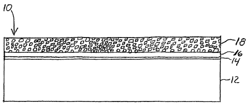
embodiments of the present invention is described. A pMUT device structure 10
comprising a
substrate 12 is provided, as illustrated in FIG. 1A. According to certain
embodiments of the
present invention, the substrate 12 is a silicon wafer. A first dielectric
film 14 is formed on the
substrate 12. In certain embodiments of the present invention, the first
dielectric film 14
comprises silicon oxide or silicon nitride. A bottom electrode layer 16 is
formed overlying the
first dielectric film 14. According to certain embodiments of the present
invention, the bottom
electrode layer 16 can comprise a metal or conductive metal oxide. A layer of
piezoelectric
material 18 is subsequently formed over the bottom electrode layer.
[0027] Piezoelectric materials that can be used in the present invention are
ceramics
including ZnO, A1N, LiNbOa, lead antimony stannate, lead magnesium tantalate,
lead nickel
tantalate, titanates, tungstates, zirconates, or niobates of lead, barium,
bismuth, or strontium,
including lead zirconate titanate (Pb(Zr,,Til_x)O3 (PZT)), lead lanthanum
zirconate titanate
(PLZT), lead niobium zirconate titanate (PNZT), BaTiO3, SrTiO3, lead magnesium
niobate, lead
nickel niobate, lead manganese niobate, lead zinc niobate, lead titanate.
Piezoelectric polymer
materials such as polyvinylidene fluoride (PVDF), polyvinylidene fluoride-
trifluoroethylene
(PVDF-TrFE), or polyvinylidene fluoride-tetrafluoroethylene (PVDF-TFE) can
also be used.
7
CA 02599399 2007-08-24
WO 2006/093913 PCT/US2006/006939
According to certain embodiments of the present invention, the layer of
piezoelectric material is
PZT.
[0028] The piezoelectric material 18 can be deposited on the pMUT device
structure 10
by physical vapor deposition (PVD), such as sputtering, chemical vapor
deposition (CVD),
molecular beam epitaxy (MBE), or by a spin coating a sol gel. 'In certain
embodiments of the
present invention, an organic solution containing lead subacetate, zirconium
acetate, and titanium
acetyl acetonate is spun onto a pMUT device structure 10, and the acetate film
is pyrolized and
annealed to form the PZT layer 18.
[0029] In certain embodiments of the present invention, spaced-apart vias 27
are formed
by etching from the front side 13 of the substrate 12 through the first
dielectric film 14 prior to
deposition of the bottom electrode layer 16, as illustrated in FIG. 1B, to
provide a path for
electrical connection between subsequently formed spaced-apart bottom
electrodes and through
wafer interconnects.
[0030] The pMUT device structure 10 is subsequently patterned, as illustrated
in FIG. 2,
by etching the layer of piezoelectric material 18 and bottom electrode layer
16 to form an array
of piezoelectric elements 22 and bottom electrodes 20. The array of
piezoelectric elements 22
can be formed by conventional photolithographic techniques, such as
photoresist deposition,
selective exposure, development, chemical or reactive ion etching, and
subsequent removal of
the exposed piezoelectric and electrode materials, according to certain
embodiments of the
present invention. In certain embodiments of the present invention,
anisotropic etching, such as
a plasma etch, is performed to provide openings 26 exposing the upper surface
of the first
dielectric film 27. In other embodiments of the present invention, a metal
lifloff process is used
to pattern the bottom electrode prior -to deposition of the piezoelectric
material. During etching
to form the separate piezoelectric elements 22, one of the piezoelectric
elements on the periphery
of the pMUT device structure 10 is further etched to remove the piezoelectric
material 18 from
the bottom electrode 20 forming a ground pad 24. In certain embodiments of the
present
invention, only one ground pad 24 is needed per pMUT device 10. In other
embodiments of the
present invention, multiple ground pads are provided for redundant electrical
connection.
[0031] A second dielectric film 28 providing acoustic and electrical isolation
between the
piezoelectric elements 22 is formed on the pMUT device structure 10 filling
the openings 26. As
illustrated in FIG. 3, the second dielectric film 28 is planarized so that its
upper surface 29 is
8
CA 02599399 2007-08-24
WO 2006/093913 PCT/US2006/006939
substantially planar with the upper surface 23 of the piezoelectric elements
22. The second
dielectric film 28 is removed above the ground pad 24, such. as by etching or
photolithography,.
forming an opening 30. The second dielectric film 28 can be a polymer. In
certain embodiments
of the present invention, the second dielectric film 28 is a polyimide,
parylene,
polydimethylsiloxane (PDMS), polytetrafluoroethylene (PTFE) or a
polybenzocyclobutene
(BCB). The use of a polymer as the second dielectric film 28 reduces inter-
element cross talk in
piezoelectric transducer arrays compared with bulk ceramic arrays that do not
have the polymer
layer between the elements. The polymer dielectric 28 attenuates acoustic
energy between the
elements 22 so that the vibration from one piezoelectric element 22 does not
affect adjacent
piezoelectric elements 22. Low interelement crosstalk has been demonstrated in
two-
dimensional pMUT arrays by employing a polymer dielectric film. Crosstalk as
low as -50dB
has been measured, compared to much higher crosstalk of -20dB for PZT ceramic
two-
dimensional arrays with no polymer dielectric between the piezoelectric
elements.
[0032] A top electrode 32 is formed overlying the piezoelectric element 22,
second
dielectric film 28, and the ground electrode 24, as illustrated in FIG. 4.
According to certain
embodiments of the present invention, the top electrode 32 comprises a metal.
According to
certain embodiments of the present invention, the top electrode 32 connects
each piezoelectric
element 22 to the ground pad 24.
[0033] The back side of the pMUT device structure 11 is selectively etched to
form
through-wafer vias 34 exposing the bottom surface of the bottom electrodes 25
forming
piezoelectric membranes 35 comprising the bottom electrodes 24 and the
piezoelectric elements
22, as shown in FIG. 5. Anisotropic etching through the substrate 12 and first
dielectric film 14
is performed using the photolithographic patterning techniques described above
and appropriate
chemical etchants for silicon wafers 12 and the first dielectric film 14 to
form the through-wafer
vias 34, according to certain embodiments of the present invention. According
to certain
embodiments of the present invention, photolithographic processes and deep
reactive ion etching
(DRIE) using an inductively coupled plasma (ICP) reactor is used to etch the
substrate 12 and
first dielectric film 14 forming through-wafer vias 34 with vertical sidewalls
3 7 in the vias. The
advantage of the DRIE process is that higher density arrays can be formed
compared with
anisotropic chemical etching, and diverse geometric element shapes can be
formed.
9
CA 02599399 2007-08-24
WO 2006/093913 PCT/US2006/006939
[0034] For pMUT structures in which the through-wafer vias 34 are formed using
a
DRIE process, substantial freedom of geometrical element shape is afforded.
Because
anisotropic chemical etching follows the crystallographic planes in silicon,
elements formed by
this method are limited to square and rectangular shapes: Elements formed by
DRIE can be
circular, square, rectangular, or other polygonal shapes. - Circular shaped
elements provide
stronger ultrasonic response at a single resonance frequency. However, for
applications
requiring higher bandwidth, square, rectangular or polygonal (e.g:, hexagonal,
octagonal) shaped
elements provide multiple overtones in the frequency response due to different
dimensions in
different geometrical directions. These overtones increase the frequency range
or, bandwidth of
the device, although at a slight decrease in sensitivity per unit area.
Bandwidth has been
measured for pMUT elements with circular shape and was found to be only 15-
20%, whereas
square elements produced measured bandwidth in the range of 50-80%. The
circular elements,
however, possessed 20-30% higher sensitivity per unit area than the square
elements.
[0035] Additionally, square, rectangular or polygonal shaped elements can be
supported
by the substrate on all sides or only some of the sides by extending the DRIE
etch beyond the
unsupported edges. For example, a square element can be supported on all four
edges by the
substrate, or can be supported only on two edges and unclamped on the other
two edges. In this
way, the piezoelectric membrane is made more flexible for larger vibrational
amplitude.
Circular elements are generally supported around the entire circumference.
Rectangular
elements with large aspect ratios (10:1 or greater) can be formed and are
generally preferable for
one-dimensional pMUT arrays, whereas elements with smaller aspect ratios
(closer to 1:1, e.g.,
square or nearly square, hexagonal, octagonal, circular) are typically formed
for two-dimensional
pMUT arrays.
[0036] Adverting to FIG. 6, a conformal insulating film 36 is deposited on the
back side
of the pMUT device structure 11, including sidewalls 37 of the through-wafer
vias 34. The
portion of the conformal insulating film 36 covering the bottom surface 25 of
the bottom
electrodes is subsequently removed, such as by etching. The conformal
insulating film 36 can
comprise conventional dielectrics such as a vapor-deposited polymer, oxide or
nitride material.
The conformal insulating film 36 is deposited by a low temperature vapor
deposition process,
such as PVD or CVD. Exposing the bottom surface 25 of the bottom electrodes
allows electrical
CA 02599399 2007-08-24
WO 2006/093913 PCT/US2006/006939
connection to the bottom electrode 24 of the piezoelectric membrane 35 without
compromising
the electrical isolation of the multiple through-wafer vias 34.
[0037] A conformal conductive film 42 is subsequently formed on the back side
of the
pMUT device structure 11. The conformal conductive film- 42 is subsequently
patterned such
that the individual through-wafer vias 34 are electrically isolated from one
another and from the
ground contact 24, as illustrated in FIG. 7A. According to certain embodiments
of the present
invention, conformal conductive film 42 comprises a metal. The conformal
conductive film 42
can be patterned by conventional photolithographic techniques to create
through-wafer
interconnects 42 in the through-wafer.vias 34. In other embodiments of the
present invention,
multiple through-wafer interconnects 42 can be electrically connected to form
larger subsets of elements that can be addressed simultaneously. These larger
element subsets are electrically
isolated from the ground via 33. For example, one-dimensional arrays can be
formed by
connecting rows of 'elements in a two-dimensional array.
[0038] .Suitable metals for use as the bottom electrode 16, top electrode 32,
and
conformal conductive film 42 include: Cr/Au, Ti/Au, Ti/Pt, Au, Ag, Cu, Ni, Al,
Pt, In, Ir, IrO2,
Ru02i In203:SnOa (ITO) and (La, Sr)Co03 (LSCO). Suitable techniques for
depositing the
metals for the bottom electrode layer 14, top electrode 32, and conformal
conductive film 42
include CVD, PVD, electroplating, electroless plating and electron beam
evaporation techniques.
According to certain embodiments of the present invention, the bottom
electrode layer 16
comprises Ti/Pt, Ir, IrOa, Ru02, or LSCO. According to certain embodiments of
the present
invention, the conformal conductive film 42 comprises CVD Cu, electroplated
Cu, or electroless
Ni or Au.
[0039] In other embodiments of the present invention, as shown in FIG. 7B,
only the
substrate 12 is etched forming through-wafer vias 34 wherein the etch stops at
the first dielectric
layer 14 exposing spaced-apart vias 17. The spaced-apart vias 17 were
previously formed by
etching from the front side'13 of the substrate 12 through the first
dielectric film 14. The spaced-
apart vias 17 are exposed again when the conformal insulating film 36 is
etched, and provide
electrical connection between the spaced-apart bottom electrodes 20 and the
subsequently
formed interconnects 42.
[0040] Adverting to FIG. 8, the pMUT device structure 10 is connected to a
semiconductor device 44 to form a vertically integrated pMUT device 60. In
certain
11
CA 02599399 2007-08-24
WO 2006/093913 PCT/US2006/006939
embodiments of the present invention, the connection is made through solder
bumps 46
connecting the conformal. conductive layer 42 to solder pads 48 on the
semiconductor device 44.
The patterned through-wafer interconnects 42 provide direct electrical
connection from the
piezoelectric membranes 35 to the semiconductor device 44. The attachment of
the
semiconductor device 44 to the pMUT device structure 10' creates air backed
cavities 50. The
air-backed cavities 50 provide optimum acoustic performance. The air-backed
cavity 50 allows
greater vibration in the piezoelectric membrane 35 with minimal acoustic
leakage compared to
surface micromachined MUTs. Vibrational energy from surface micromachined
membranes can
be dissipated into the bulk silicon substrate which resides directly below the
membrane thus
limiting the ultrasonic transmit output and receive sensitivity. The air
backed cavity 50 of the
present invention reduces or eliminates this energy dissipation since the
vibrating membrane 35
does not reside directly on or over the bulk substrate 12.
[0041] The semiconductor device 44 can be any semiconductor device known in
the art,
including a wide variety of electronic devices, such as flip-chip package
assemblies, transistors,
capacitors, microprocessors, random access memories, etc. In general,
semiconductor devices
refer to any electrical device comprising semiconductors. In certain
embodiments of the present
invention, the semiconductor device 44 is a CMOS chip.
[00421 Because each piezoelectric element 22 is electrically isolated from
adjacent
piezoelectric elements 22, the individual elements can be separately driven in
the transducer
transmit mode. Additionally, receive signals can be measured from each
piezoelectric membrane
35 independently by the semiconductor device 44.
[0043] An advantage of the formation of the through-wafer interconnects 42 is
that
separate wires, flex cable, etc., are not required to carry electrical
transmit and receive signals
between the membranes 35 and semiconductor device 44, as electrical connection
is provided
directly by the interconnects 42. This reduces the number of wires and size of
the cabling
required to connect the ultrasonic probe to a control unit. Furthermore, the
shorter physical
length of the through-wafer interconnects 42 (on the order of 100 m to a few
mm) compared
with conventional cable or wire harnesses (length on the order of meters)
provides connections
with lower resistance and shorter signal path which minimizes loss of the
transducer receive
signal and lowers the power required to drive the transducers for transmit.
12
CA 02599399 2007-08-24
WO 2006/093913 PCT/US2006/006939
[0044] The use of metal interconnects 42 and electrodes 20, 32 provide a
piezoelectric
device with higher. electrical conductivity and higher signal-to-noise ratio
than devices using
polysilicon interconnects and electrodes. In addition, the use of low
temperature processes of
depositing the conformal insulating layer 36 and conformal conductor 42
reduces the thermal
budget of the device processing, thus limiting the 'damaging'effects of
excessive exposure to
heat. This also allows the pMUT elements 22 to be formed before etching the
through-wafer via
holes 34 in the substrate, thus simplifying the overall processing.
[0045] In certain embodiments of the present invention; a polymer coating 52
is formed
on the surface of the semiconductor device 45, or at the base of the air-
backed cavity 50, as
shown in FIG. 9. The polymer layer 52 attenuates acoustic energy reflected
from the
piezoelectric membrane 35. When a pMUT device structure 10 is attached
directly to a
semiconductor device substrate 44, there is observed some reverberation of the
pMUT element
22 as acoustic energy is reflected off of the semiconductor device substrate
44 and directed back
toward the piezoelectric membrane 35. The reverberation causes noise in the
pMUT signal and
reduces ultrasound image quality. Also the acoustic energy could affect
semiconductor device
operation by introducing noise in the circuit. Without the polymer attenuating
layer 52, a
resonant cavity condition is created which causes excessive ringing or
reverberations in the
transducer membrane 35. By providing a polymer layer 52 on top of the
semiconductor device
44 or at the base of the air-backed cavity 50, acoustic energy reflected from
the pMUT device
structure 10 is attenuated by the polymer layer 52. The polymer layer 52 has
lower acoustic
impedance and therefore reflects less ultrasonic energy than a bare silicon
surface of the
semiconductor device with high acoustic impedance. In certain embodiments of
the present
invention, the polymer layer 52 can also function as an adhesive for
atta.chment of the pMUT
device structure 10 to the semiconductor device 44. In certain embodiments of
the present
invention, the polymer layer 52 comprises an epoxy.
[0046] The thickness of piezoelectric elements 22, in certain embodiments of
the present
invention, can range from about 0.5 m to about 100 . m. In certain
embodiments of the present
invention, the thickness of the piezoelectric elements 22 ranges from about 1
m to about 10 m.
The width or diameter of the piezoelectric elements 22 can range from about 10
m to about 500
m with center-to-center spacing from about 15 gm to about 1000 m. In certain
embodiments
of the present invention, the width or diameter of the piezoelectric elements
22 can range from
13
CA 02599399 2007-08-24
WO 2006/093913 PCT/US2006/006939
about 50 gm to about 300 m with center-to-center spacing from about 75 m to
450 m for
ultrasonic operation in the range of I to 20 MHz. In other embodiments of the
present invention,
smaller elements of less than 50 m can be patterned- for higher frequency
operation of >20
MHz. In this case, multiple elements may be electrically connected together to
provide higher
ultrasonic energy output while still maintaining the high frequency of
operation.
[0047] The thickness of the first dielectric film 14, in certain embodiments
of the present
invention, can range from about 10 nm to about 10 .m.. In certain embodiments
of the present
invention, the thickness of the conformal insulating film 36 ranges from about
10 nm to about 10
m. The thickness of the bottom electrode 20, top electrode 32, and conformal
conductive layer
42 ranges from about 20 nm to about 25 m. The depth of the open cavity 50, in
certain
embodiments of the present invention, can range from about 100 grii to several
mm.
[0048] In certain embodiments of the present invention the pMUT device
structure 10 is
connected to the semiconductor device 44 through metal contacts 54 formed in
the epoxy layer
56 on the semiconductor device 44, as illustrated in FIG. 10. The epoxy layer
56, in addition to
functioning as an' acoustic energy attenuator, also functions as an adhesive
for adhering the
pMUT device structure 10 to the semiconductor device 44. The epoxy layer 56
can be patterned
using photolithographic and/or etching techniques, and metal contacts can be
deposited by
electroplating, sputtering, e-beam evaporation, CVD, or other deposition
methods.
[0049] The second dielectric film 28 is disposed on the top edges 58 of the
piezoelectric
elements in certain embodiments of the present invention, as illustrated in
FIG. 11. The pMUT
device structure 80 is subsequently processed, including back side etching, as
previously
described and connected to a semiconductor device 44 to form a vertically
integrated
piezoelectric micromachined ultrasonic transducer device 90, as illustrated in
FIG. 12. The
second dielectric film 28 'on the top edges of the patterned piezoelectric
layer 58 provides
improved electrical isolation of the two electrodes 32, 20 connected to the
piezoelectric elements
22. This embodiment helps account for any photolithography misalignment which
could
inadvertently cause a gap between the polymer dielectric 28 and piezoelectric
layer 22 edges
causing the top electrode 32 to short to the bottom electrode 20. It also
eliminates the need for
any planarization processes that might be required in other embodiments. This
embodimeiit
further provides a method of forming a size or shape of the top electrode 32
that is different from
the size and shape of the patterned piezoelectric layer 22. If thick enough
(on the order of the
14
CA 02599399 2007-08-24
WO 2006/093913 PCT/US2006/006939
piezoelectric thickness), the polymer dielectric 28 with much lower dielectric
constant than the
piezoelectric layer 22 causes the voltage applied to the pMUT 90 device to
primarily drop only
across the dielectric, thus electrically isolating the portion of the
piezoelectric layer 58 that is
covered with the dielectric. The effective shape of the piezoelectric element
22 with regard to
the applied voltage is only the portion of the piezoelectric layer 22 that is
not covered with the
dielectric. For example, if it is desired only to electrically activate 50% of
the total piezoelectric
geometrical area, then polymer dielectric 28 can physically cover and
electrically isolate the
remaining 50% of the piezoelectric area and prevent it from being activated.
Also if a complex
electrode pattern is desired such as an interdigitated structure, the polymer
dielectric 28 can be
patterned to provide the interdigitated structure. This is important for
certain embodiments
wherein the top electrode 32 is a continuous ground electrode across the
entire pMUT array 90.
Simpler processing is provided by creating the. electrically active area by
patterning the polymer
dielectric 28, thus the active area assumes the shape of the top electrode
area contacting the
piezoelectric fihn 16, rather than patterning the bottom electrode 20 and
piezoelectric film 16.
[0050] Certain embodiments of the present invention use a silicon-on-insulator
(SOI)
substrate as the substrate. As shown in FIG. 13, a substrate 12, such as a
silicon wafer, is
provided with a thin silicon layer 62 overlying a buried silicon dioxide layer
64 formed on the
substrate 12. A first dielectric film 14 is formed overlying the silicon layer
62 and a bottom
electrode layer 16 is formed overlying the first dielectric film. A layer of
piezoelectric material
18 is formed overlying the bottom electrode layer 16 to provide a SOI pMUT
device structure
100. Advantages of using the SOI substrate include better control of the DRIE
etch using the
buried oxide as the silicon substrate etch stop. This also provides better
control of the pMUT
membrane 35 thickness for better control and u.niformity of the resonance
frequencies of the
individual elements in an array, as the membrane thickness is defined by the
thickness of the thin
silicon layer of the SOI substrate 62. According to certain embodiments of the
present invention,
the thin silicon layer 62 has thickness of about 200 nm to 50 m, and the
buried oxide layer 64
has thickness of about 200 nm to 1 pm. In other embodiments of the present
invention, the thin
silicon layer 62 has thickness of about 2 m to 20 m, and the buried oxide
layer 64 has
thickness of about 500 nm to 1 m.
[0051] The layer of piezoelectric material 18, bottom electrode layer 16,
first dielectric
film 14, silicon layer 62, and buried silicon oxide layer 64 are subsequently
etched to provide
CA 02599399 2007-08-24
WO 2006/093913 PCT/US2006/006939
s.eparate piezoelectric elements 22 and a ground pad 24, and to expose the
front side 13 of the
substrate 12. The piezoelectric 18 and bottom electrode 16 layers are etched
to form the pMUT
element shape 32 separated by openings 68. The first dielectric 14, thin
silicon 62, and buried
oxide 64 layers are further etched to form spaced-apart vias 69 exposing the
substrate 12. A
conductive film 66 is deposited in the spaced-apart vias 69; as illustrated in
FIG. 14, to provide
electrical connection between the bottom electrode 20 and the through-wafer
interconnects to be
subsequently formed. Patterriing of the pMUT device structure 100 can be done
using
conventional photolithographic and etching techniques, as previously
described. In certain
embodiments of the present invention, the conductive film 66 can be any of the
metals described
above with respect to the bottom electrode 20, top electrode 32, and conformal
conductive layer
42.
[0052] The SQI pMUT device structure 100 is further processed, as previously
explained
with respect to the other embodiments of pMUT devices, to form the second
dielectric film 28,
top electrode 32, through-wafer vias 34, conformal insulating layer 36, and
conformal
conductive film 42, as illustrated in FIG. 15. Electrical contact between the
conductive film 66
and the conformal conductive film 42 provide a through-wafer interconnect. The
SOI pMUT
device structure 100 is connected to a semiconductor device 44, such as
through solder bumps
46, as shown in FIG.15, to form a vertically integrated pMUT device 110. In
other
embodiments, the semiconductor device 44 can be electrically connected to the
conformal
conductive film 42 through metal contacts formed in an epoxy layer deposited
on the surface of
the semiconductor device which attaches the pMUT device to the semiconductor
device, as
previously described.
[00531 Uses for pMUTs formed according to the present invention include real
time,
three-dimensional intracardiac or intravascular imaging, imaging for minimally
invasive or
robotic surgeries, catheter-based imaging, portable ultrasound. probes, and
miniature
hydrophones. In certain embodiments of the present invention, the pMUTs are
optimized for
operation in the frequency range of about 1-20 MHz.
[0054] The embodiments illustrated in the instant disclosure are for
illustrative purposes.
They should not be construed to limit the scope of the claims. As is clear to
one of ordinary skill
in this art, the instant disclosure encompasses a wide variety of embodiments
not specifically
illustrated herein.
16