Note: Descriptions are shown in the official language in which they were submitted.
CA 02600471 2008-11-06
METHOD AND APPARATUS FOR CUSTOMIZATION
OF A PROTECTIVE DEVICE
Background of the Invention
The present invention generally relates to power system protection, and
more specifically, to a method and apparatus for customization of a protective
device.
Electric utility systems or power systems are designed to generate,
transmit and distribute electrical energy to loads. In order to accomplish
this,
power systems generally include a variety of power system elements such as
electrical generators, electrical motors, power transformers, power
transmission
lines, buses and capacitors, to name a few. As a result, power systems must
also include protective devices and procedures to protect the power system
elements from abnormal conditions such as electrical short circuits,
overloads,
frequency excursions, voltage fluctuations, and the like.
Protective devices and procedures act to isolate some power system element(s)
from the remainder of the power system upon detection of the abnormal
condition or a fault in, or related to, the power system element(s). Logically
grouped zones of protection, or protection zones utilizing the protective
devices
and procedures, are established to efficiently manage faults or other abnormal
conditions occurring in the power system elements.
Generally, protective devices are also used for protecting, monitoring,
controlling, metering and/or automating electric power systems and associated
transmission lines. Protective devices may include protective relays, remote
terminal units (RTUs), power line communications devices (PLCs), bay
controllers, supervisory control and data acquisition (SCADA) systems, general
computer systems, meters, and any other comparable devices used for
protecting, monitoring, controlling, metering and/or automating electric power
systems and their associated transmission lines.
-1-
CA 02600471 2008-11-06
Traditional protective devices generally include various overcurrent,
voltage, directional, distance, differential, and frequency protective logic
schemes. These logic schemes and the logic elements associated therewith are
generally either programmed into user programmable memory or permanently
hard coded into fixed memory. Protective devices require flexibility and
modification in their processing based on their application in the field.
Often,
protective device applications are unique in nature. Accordingly,
modifications
to protective devices used in such applications are similarly unique for a
particular user.
In traditional protective devices, some modifications in device processing
can be made by the end user (e.g., the customer) by modifying the user
programmable memory. For example, the end user may modify the user
programmable memory to include custom logic algorithms. Nevertheless, for
some complex applications, modification of user programmable memory is
insufficient due to inadequate microprocessor capacity or inadequate free
volatile
memory.
Another traditional approach to modification of protective device
processing involves changes in the fixed memory contained permanently in the
device. Such fixed memory is alternatively referred to as firmware.
Modification
of the firmware generally involves changes by the programmer (e.g., the
manufacturer) requiring extensive product validation and manufacturing release
processes. These validation and release processes are often complicated,
costly,
and burdensome for both the end user (e.g., customer) and the programmer
(e.g., manufacturer).
The cost for modification of firmware in protective devices ranges from a
few thousands of dollars, which is rare, to several hundred thousands of
dollars,
which is more common. Therefore, the manufacturer must weigh whether any
increase in sales volume and/or revenue expected from each change would
warrant the costs for research, development and implementation of each
individual firmware modification. Because modifications are often unique in
nature, these costs often do not warrant manufacturer changes for unique
applications.
-2-
CA 02600471 2008-11-06
In yet another traditional approach to modification of protective device
processing, a separate computing platform may be connected to a protective
device in order to control device processing. Nevertheless, traditional
operating
systems for these computing platforms do not have the capacity to execute
device processing within a desired time. For example, the computer is unable
to
execute device processing within the required operation time for the
protective
device to execute protection, monitoring, control, metering and/or automation
of
electric power systems and associated transmission lines (e.g. isolating an
abnormal condition in the power system as soon as possible so as to not cause
damage within the system). The fast processing time required is generally
about 4-5 milliseconds.
Thus, it is an object of this invention to provide a method and apparatus
which customizes protective devices for all applications. It is further an
object of
this invention to provide a method and apparatus for customizing a protective
device without modifying the device's firmware.
These and other desired benefits of the preferred embodiments, including
combinations of features thereof, of the invention will become apparent from
the
following description. It will be understood, however, that a process or
arrangement could still appropriate the claimed invention without
accomplishing
each and every one of these desired benefits, including those gleaned from the
following description. The appended claims, not these desired benefits, define
the subject matter of the invention. Any and all benefits are derived from the
multiple embodiments of the invention, not necessarily the invention in
general.
Summary of the Invention
In accordance with the invention, an apparatus for customization of a
protective device having a microprocessor for processing select logic schemes
is
provided. The apparatus generally includes programmer programmable memory
coupled to the microprocessor. The programmer programmable memory
includes elements associated with some of the select logic schemes to be
-3-
CA 02600471 2008-11-06
processed by the microprocessor and adapted to be modifiable by only a
programmer of said protective device.
In accordance with another embodiment of the invention, an apparatus for
customization of a protective device is provided including a microprocessor
for
processing select logic schemes. Coupled to the microprocessor are a user
programmable memory, fixed memory, and programmer programmable
memory. The user programmable memory includes elements associated with
some of the select logic schemes and is adapted to be modifiable by a user of
said protective device. The fixed memory is generally unmodifiable and
includes
elements associated with some of the select logic schemes. The programmer
programmable memory includes elements associated with some of the select
logic schemes to he processed by the microprocessor and is adapted to be
modifiable by only a programmer of the protective device. The elements
associated with the programmer programmable memory are implemented in the
form of a compiled settings structure including a plurality of allocation
fields.
In accordance with yet another aspect of the invention, provided is a
method for customizing a protective device including the steps of coupling
programmer programmable memory to a microprocessor, adapting the
programmer programmable memory to he modifiable by only a programmer of
said protective device; implementing elements associated with some of the
select logic schemes in the form of a compiled settings structure having a
plurality of allocation fields into the programmer programmable memory;
implementing executable code into at least one of the allocation fields; and
designating at least one of the allocation fields as a pointer allocation
field for
specifying a point at which portions of said code is to be executed by the
microprocessor.
It should be understood that the present invention includes a number of
different aspects or features which may have utility alone and/or in
combination
with other aspects or features. Accordingly, this summary is not exhaustive
identification of each such aspect or feature that is now or may hereafter be
claimed, but represents an overview of certain aspects of the present
invention
to assist in understanding the more detailed description that follows. The
scope
-4-
CA 02600471 2008-11-06
of the invention is not limited to the specific embodiments described below,
but
is set forth in the claims now or hereafter filed.
Brief Description of the Drawings
Figure 1 is a single line schematic diagram of a power system that may he
utilized in a typical metropolitan area.
FIGURE 2 is a block diagram of a protective relay coupled to the
protection zone of the power system of FIG. 1 according to an embodiment of
the invention.
FIGURE 3 is a block diagram of an exemplary configuration of a traditional
protective relay of FIG. 2.
FIGURE 4 is a block diagram of an exemplary configuration of an
alternative protective relay having programmer programmable memory in
accordance with an aspect of the present invention, which may he used in place
of the traditional protective relay of FIG. 3.
FIGURE 5 illustrates a detailed structural diagram of a compiled settings
code and data structure implemented in the programmer programmable memory
of FIG. 4 in accordance with an aspect of the present invention.
FIGURE 6 illustrates a detailed structural diagram of volatile memory
associated with the programmer programmable memory of FIG. 4.
Detailed Description of the Invention
The present invention generally relates to a method and apparatus for
customization of a protective device. Generally, protective devices are used
for
protecting, monitoring controlling, metering and/or automating electric power
systems and associated transmission lines. Protective devices may include
protective relays, RTUs, PLCs, bay controllers, SCADA systems, general
computer systems, meters, and any other comparable devices used for
-5-
CA 02600471 2008-11-06
protecting, monitoring, controlling, metering and/or automating electric power
systems and their associated transmission lines.
Protective devices generally include various overcurrent, voltage,
directional, distance, differential, and frequency protective logic schemes.
In
accordance with an aspect of this invention, these logic schemes and the logic
elements associated therewith are generally either programmed into user
programmable memory, programmed into programmer programmable memory,
or permanently hard coded into fixed memory. In accordance with the teachings
of the present invention, the programmer programmable memory allows for
flexibility and modification in protective device processing based on their
application in the field.
Although the embodiments described herein are associated with protective
relays, it is contemplated that the embodiments may also he associated with
any
suitable power system control or protective devices such as those described
above or below.
For example, in one application a protective relay may be used to protect
and monitor a power system. More specifically, FIGURE 1 is a single line
schematic diagram of a power system 10 that may be utilized in a typical
metropolitan area. As illustrated in FIG. 1, the power system 10 includes,
among other things, two generators 12 configured to generate three sinusoidal
waveforms, for example, three 12 kV sinusoidal waveforms, two step-up
transformers 14 configured to increase the 12 kV sinusoidal waveforms to a
higher voltage such as 345 kV and a number of circuit breakers 18. The step-up
transformers 14 provide the higher voltage sinusoidal waveforms to a number of
long distance transmission lines such as the transmission lines 20.
In one embodiment, a first substation 15 may be defined to include the
generators 12, the step transformers 14, and the circuit breakers 18, all
interconnected via a first bus 19. At the end of the long distance
transmission
lines 20, a second substation 22 includes step-down transformers 24 to
transform the higher voltage sinusoidal waveforms to lower voltage sinusoidal
-6-
CA 02600471 2008-11-06
waveforms (e.g. 15 kV) suitable for distribution via a distribution line 26 to
various end users and loads.
As previously mentioned, the power system 10 includes protective devices
and procedures to protect the power system elements from faults or other
abnormal conditions. As will he discussed in further detail below, the
protective
devices and procedures utilize a variety of protective logic schemes to
determine
whether a fault or other problem exists in the power system 10. In traditional
protective relays, these logic schemes are either programmed into user
programmable memory or permanently hard coded into fixed memory. In
accordance with the teachings of the present invention, these logic schemes
may
additionally be programmed into programmer programmable memory.
In one example of utilization of a logic scheme, some types of protective
relays utilize a current differential comparison to determine whether a fault
exists in the protection zone. Other types of protective relays compare the
magnitudes of calculated fundamental phasors, representative of the three
sinusoidal waveforms, to determine whether a fault exists in the protection
zone
Frequency sensing techniques and harmonic content detection is also
incorporated in protective relays to detect fault conditions. Similarly,
thermal
model schemes are utilized by protective relays to determine whether a thermal
problem exists in the protection zone.
Referring again to FIG. 1, a protection zone 16 is established to include a
portion of the first substation 15. A protective relay is coupled to the
protection
zone 16 via a number of current transformers.
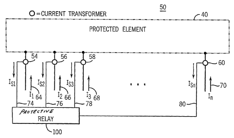
FIG. 2 is a block diagram of a protective relay 100 coupled to the
protection zone 16 of FIG. 1 according to an embodiment of the invention.
Although only one protection zone 16 is included for ease of discussion, the
power system 10 may include many overlapping protection zones. Referring to
FIGS. 1 and 2, the protection zone 16 is configured to protect a portion of
the
first substation 15 via operation of the protective relay, coupled to the
protection
zone via no current transformers 54, 56, 58 to 60. For ease of discussion, the
protective relay is configured as a protective relay 100, adapted to monitor
only
-7-
CA 02600471 2008-11-06
the A-phase primary currents flowing into the protection zone 16. Thus, two
additional protection zones having the same "footprint," may also be
configured
with two additional respective protective relays to monitor the B-phase base
and
C-phase currents flowing into corresponding protection zones. Alternatively,
one
protective relay may be configured to monitor more than one protection zone.
Although illustrated using the protective relay 100, it should be noted that
other types of protective devices (e.g., a general computer) may be utilized
to
implement the apparatus and methods disclosed herein. Further, although
illustrated as four current transformers, it should be noted that nn current
transformers 54, 56, 58 to 60 represent all of the current transformers
required
to couple the protective relay 100 to the protection zone 16.
As previously mentioned, the protection zone 16 may he defined such that
the protective relay 100 utilizes the A secondary current waveforms of the
current transformers. Thus, each of the nn current transformers 54, 56, 55 to
60 is configured to step the current magnitudes of respective A-phase primary
current waveforms 64, 66, 68 to 70 to corresponding secondary current
waveforms 74, 76, 78 to 80, having magnitudes suitable for use by the
protective relay 100. Further, each of the A-phase primary current waveforms
64, 66, 68 to 70 is equal to respective corresponding secondary current
waveforms 74, 76, 78 to 80, multiplied by respective current transformer
ratios
(turn ratios) of the respective current transformers 54, 56, 58 to 60. For
example, or
It=x''
77' where nl is in the turn ratio of the current transformer 54.
During operation and protection of protected element 40 located in
protection zone 16, the protective relay 100 processes the secondary current
waveforms 74, 76, 78 to 80 received via respective current transformers 54,
56,
58 to 60. The secondary current waveforms 74, 76, 78 to 80 are filtered,
sampled and then digitized for use by a microprocessor (or a field
programmable
gate array (FPGA)) of the protective relay 100. The microprocessor then
calculates a series fundamental phasors, each having a magnitude and phase
-8-
CA 02600471 2008-11-06
angle that are representative of each of the A-phase primary current waveforms
64, 66, 68 to 70, and then performs calculations to determine if a short
circuit or
fault exists in the protection zone 16.
For example, FIG. 3 is a block diagram of an exemplary configuration of a
traditional protective relay 100a that may be used in place of protective
relay
100 of FIG. 2 where the secondary current waveforms 74a, 76a, 78a to 80a are
illustrated as Iasi, I4,2, Iasi to IAsmm. Although only secondary current
waveforms
74a, 76a, 78a to 80a are shown in FIG 3, it should be noted that all secondary
current waveforms (i.e., CT signals) of the current transformers 54, 56, 58 to
60
are included.
Referring to FIG, 3, during operation, the secondary current waveforms
74a, 76a, 78a to 80a received by the traditional protective relay 100a are
further transformed into corresponding current waveforms via respective
current
transformers 102a, 104a, 106a, to 108a and resistors (not separately
illustrated), and filtered via respective analog low pass filters 112a, 114a,
116a
to 118a. An analogue-to-digital (AID) converter 120a then multiplexes, samples
and digitizes the filtered secondary current waveforms to form corresponding
digitized current sample streams (e.g., 1011001010001111).
The corresponding digitized current sample streams are received by a
microcontroller 130, where they are digitally filtered via, for example, a
pair of
Cosine filters to eliminate DC and unwanted frequency components.
Microcontroller 130 may also be adapted to receive signals via binary inputs
132a from other external devices such as protective devices or external
computers.
In this traditional relay, the microcontroller 130 includes a
microprocessor, or CPU 134, a user programmable memory 136, and fixed
memory 138. The traditional relay is adapted to implement overcurrent,
voltage, directional, distance, differential, and frequency protective logic
schemes. These logic schemes and the logic elements associated therewith are
generally either programmed into user programmable memory 136 or
permanently hard coded into fixed memory 138. The microprocessor 134 is
-9-
CA 02600471 2008-11-06
coupled to the user programmable memory 136 and the fixed memory 138 so
that it may access the logic schemes and logic elements associated therewith
in
order to perform various protective functions.
More specifically, the user programmable memory 136 may include
operators, inputs, outputs, algorithms, and logic which may be programmable by
the user (e.g., the customer) in order to achieve a particular logic scheme.
Modifications in device processing can be made by the end user (.g., the
customer) by modifying the user programmable memory 136. Nevertheless, for
some complex applications, modification of user programmable memory 136 is
insufficient due to inadequate microprocessor capacity or inadequate free
volatile
memory. Modification of user programmable memory 136 may further involve
complex programming of logic and elements related thereto in order to achieve
cooperation with logic already existing within user programmable memory 136
or within fixed memory 138.
Fixed memory 138 may further include operators, inputs, outputs,
algorithms, and logic which are preprogrammed by the programmer (e.g., the
manufacturer) in order to achieve a particular logic scheme. Unlike the user
programmable memory 136, fixed memory 138 (e.g., firmware) is intended to
be contained permanently in the device and may not be altered by the end user.
Fixed memory 138 is intended to include operators, inputs, outputs,
algorithms,
and logic for essential device functions. For example, threshold or timer
settings
are often found in fixed memory 138.
Modification of the fixed memory 138 generally involves a firmware
update by the programmer (e.g., the manufacturer). Because of the critical
nature of protective device processing, any firmware updating requires
extensive
product validation and manufacturing release processes. This validation and
release processes are often complicated, costly, and burdensome for both the
end user (e.g., customer) and the programmer (e.g., manufacturer). The cost
for modification of firmware in protective devices ranges from a few thousands
of dollars, which is rare, to several hundred thousands of dollars, which is
more
common. Therefore, the manufacturer must weigh whether any increase in
sales volume and/or revenue expected from each change would warrant the
-10-
CA 02600471 2008-11-06
costs for research, development and implementation of each individual firmware
modification. Because modifications are often unique in nature, these costs
often do not warrant manufacturer changes for unique applications.
In yet another traditional approach to modification of protective device
processing, a separate computing platform may be connected to a protective
device in order to control device processing. In this arrangement, the
computing
platform would provide input signaling via binary inputs at 132 to augment
various microcontroller functions. Nevertheless, traditional operating systems
for these computing platforms do not have the capacity to execute device
processing within a desired 4-5 milliseconds. The required fast processing
time
is due to a desired operation time of the protective device to execute
protection,
monitoring, control, metering and/or automation of electric power systems and
associated transmission lines (e.g., isolating an abnormal condition in the
power
system as soon as possible so as to not cause damage within the system).
In order to overcome the shortcomings of modification of protective
device processing as described with regard to FIGURE 3, microcontroller 140 in
accordance with an aspect of the current invention as illustrated in FIGURE 4
may replace the microcontroller 130 of FIGURE 3.
More specifically, FIG. 4 is a block diagram of an exemplary configuration
of a protective relay 100b in accordance with an aspect of the current
invention.
Protective relay 100b may generally comprise a similar structure as the
protective relay 100a of Figure 1, except for microcontroller 140 of Figure 4
as
compared to microcontroller 130 of Figure 3. Therefore, the secondary current
waveforms 74b, 76b, 78b to 80b received by the protective relay 100b are
transformed into corresponding current waveforms via respective current
transformers 102b, 104b, 106b, to 108b and resistors (not separately
illustrated), and filtered via respective analog low pass filters 112b, 114b,
116b
to 118b. An analog-to-digital (A/D) converter 120b then multiplexes, samples
and digitizes the filtered secondary current waveforms to form corresponding
digitized current sample streams (e.g., 1011001010001111).
- 11 -
CA 02600471 2008-11-06
The corresponding digitized current sample streams are received by a
microcontroller 140, where they are digitally filtered via, for example, a
pair of
Cosine filters to eliminate DC and unwanted frequency components.
Microcontroller 140 may also be adapted to receive binary inputs 132b from
other external devices such as protective devices or external computers.
Binary
inputs 132b may include, among other things, data streams as those described
in US. Patent No. 5,793,750 for "System for Communicating Output Function
Status Indications Between Two or More Power System Protective Relays" and
Patent No, 6,947,629 for "Relay-to-Relay Direct Communication System in an
Electric Power System".
In this relay in accordance with an aspect of the present invention, the
microcontroller 140 includes a microprocessor, or CPU 142, a user
programmable memory 144, programmer programmable memory 146, and fixed
memory 148. The relay is adapted to implement overcurrent, voltage,
directional, distance, differential, and frequency protective logic schemes.
These
logic schemes and the logic elements associated therewith are generally either
programmed into user programmable memory 144, programmed into
programmer programmable memory 146, or permanently hard coded into fixed
memory 148. The microprocessor 142 is coupled to the user programmable
memory 144, the programmer programmable memory 146, and the fixed
memory 138 so that it may access the logic schemes and logic elements
associated therewith in order to perform various protective functions.
More specifically, the user programmable memory 144 may include
operators, inputs, outputs, algorithms, and logic which may be programmable by
the user (e g., the customer) in order to achieve a particular logic scheme.
Modifications in device processing can be made by the end user (e.g., the
customer) by modifying the user programmable memory 144. Such modification
is intended for routine applications, which do not hinder microprocessor
capacity
nor require a large amount of free volatile memory.
Fixed memory 148 may include operators, inputs, outputs, algorithms,
and logic which are preprogrammed by the programmer (e.g. the manufacturer)
in order to achieve a particular logic scheme. Unlike the user programmable
-12-
CA 02600471 2008-11-06
memory 144, fixed memory 148 (e.g., firmware) is intended to be contained
permanently in the device and may not be altered by the end user. Fixed
memory 148 is intended to include operators, inputs, outputs, algorithms, and
logic for essential device functions. For example, threshold or timer settings
may be stored in fixed memory 146.
Programmer programmable memory 146 is a nonvolatile memory location
which may include operators, inputs, outputs, algorithms, and logic
programmable by the programmer (e.g., the manufacturer) in order to achieve a
particular logic scheme. For example, such logic elements for a particular
logic
scheme are saved in the form of compiled settings within programmer
programmable memory 146. In one embodiment, the compiled settings may be
downloaded in compiled settings file format, decoded, and saved to the
programmer programmable memory 146 in executable form. In turn, the
microprocessor 140 retrieves the compressed compiled settings code and data,
and temporarily saves the code and data associated therewith into a volatile
memory location. The processing of the code and data from programmer
programmable memory 146 is handled in an analogous fashion as the data from
user programmable memory 144, once the data from user programmable
memory has been compiled.
FIGURE 5 illustrates a detailed structural diagram of compiled settings
code and data structure implemented in the programmer programmable memory
146 of FIG. 4 in accordance with an aspect of the present invention. In this
embodiment, the programmable memory includes a compiled settings structure
for organizing logic elements (e.g. operators, inputs, outputs, algorithms,
logic
and the like) associated with a particular logic scheme into select allocation
fields. For example, the compiled settings structure may include an allocation
field for specifying "Relay Type" 150. This allocation field specifies the
type of
relay associated with the compiled settings, thereby allowing the
microprocessor
to check this allocation field to ensure the particular compiled settings is
appropriate. For example, the microprocessor compares this "relay type"
allocation field with an associated element in the fixed memory, thereby
ensuring that the particular compiled settings is appropriate. Without
deviating
- 13 -
CA 02600471 2008-11-06
from the teachings of the present invention, this allocation field may
alternatively specify any other protective device.
A "Reference Number" 152 allocation field is provided for specifying the
specific version of relay, otherwise referred hereinafter as "relay word",
associated with the compiled settings. The microprocessor further checks this
allocation field to ensure that the compiled settings will not cause an
internal
conflict or problem related thereto. For example, the microprocessor compares
this "reference number" allocation field with an associated element in the
fixed
memory, thereby ensuring that the particular compiled settings is appropriate
and will not cause an internal conflict related thereto. Any relay word
conflicts
may thereupon be signaled at settings save time and at settings change time.
Without deviating from the teachings of the present invention, this allocation
field may alternatively specify any other protective device.
A "Max Execution Time" 154 allocation field is provided for specifying how
long associated code in the compiled settings will take to execute, thereby
enabling the microcontroller to calculate the total execution time for all
compiled
settings downloaded in the programmer programmable memory. This enables
the relay to ensure that the execution time does not exceed a select threshold
stored in the fixed memory. Generally, this threshold is programmed and
established by relay designers to ensure all algorithms complete in the
allocated
time. This time may further be used to calculate the processing rate needed to
support the compiled settings via an algorithm stored in the fixed memory.
An "ID String for VER command" 156, or alternatively a "SHO command,"
allocation field is provided for specifying a listing and description of
compiled
settings stored in the in programmer memory 146, thereby allowing the user to
determine what algorithms are loaded into programmer memory 146. A "Digital
Signature" 158 allocation field specifies the origin of the compiled settings.
With
this allocation field, the user may compare the digital signature value to a
value
published by the programmer to ensure that the compiled settings originated
from that programmer. The microprocessor further calculates a digital
signature
for the compiled settings, and compares it to a digital signature stored in
the
fixed memory. If the digital signature and stored digital signature do not
match,
-14-
CA 02600471 2008-11-06
the microcontroller provides a binary output signal to signal such. This
binary
output signal may ultimately be used to signal an error at settings change or
download time.
The compiled settings structure may further include pointer allocation
fields for specifying a point at which portions of executable code is to be
executed by the microprocessor. A "Cold Initialization Code Pointer" 160
allocation field is provided for specifying a pointer to the associated code
that
requires execution at power or other cold initiation times. A "Warm
Initialization
Code Pointer" 162 allocation field specifies a pointer to the associated code
that
requires execution at a settings change or other warm initiation times (e.g.,
for
performing actions such as initialization of binary outputs). A "Run Time Code
Pointer" 164 allocation field is provided for specifying a pointer to
associated
code that is executed every processing interval. This associated code is
analogous to certain compiled code in user programmable memory. A "Settings
Validation Code Pointer" 166 allocation field specifies a pointer to
associated
code that verifies the validity of any new settings used by the compiled
settings
to allow user entered parameters.
A "Code Space" 168 field allocation contains all of associated code
mentioned in the previous paragraph. An "Output Element List" 170 field
allocation is provided for specifying, preferably in listing format, the logic
elements, as designated by the "Reference Number" 152 allocation field, that
are
being modified by the code contained in 168. In one embodiment, this list can
be used to customize a user interface associated therewith.
A "Settings Structures" 172 allocation field contains any compiled settings
which require comparison with thresholds. The microprocessor uses settings
routines stored in the fixed memory coupled with this allocation field to
prompt
for, check the limits of, and store new settings required by the code
contained in
168. A "Default Settings" 174 allocation field is further provided comprising
default values for the new settings defined in the "Settings Structures" 172.
Without deviating from the teachings of the current invention, a plurality
of compiled settings structures as outlined above may be implemented in
- 15 -
CA 02600471 2008-11-06
programmer programmable memory. Moreover, each such compiled setting
structure may include any or all of the allocation fields described above. A
number of other allocation fields comprising additional logic elements not
discussed herein may also be included. For example, the programmer
programmable memory may include a compiled settings structure having any of
the allocation fields as discussed above coupled with yet another compiled
settings structure having a similar or even different allocation fields.
FIGURE 6 illustrates a detailed structural diagram of volatile memory or
random access memory (RAM) 180 associated with the programmer
programmable memory in accordance with an aspect of the present invention.
In this embodiment, the volatile memory includes a plurality of allocation
fields.
For example, the "Global/Static Variables" 182 allocation field provides a
temporary copy of user entered parameters and variables required by the
programmer programmable memory 146. The "Unsolicited Write Database Size"
184 allocation field contains the size of the "Database" field that is used by
the
programmer programmable memory 146.
The "Unsolicited Write State" 186 allocation field is used for arbitration of
the "Unsolicited Write Address" 188 allocation field, the "Unsolicited Write
Length" 190 allocation field, and the "Unsolicited Write Register" 194
allocation
field between the fixed memory code 148 and the programmer programmable
memory code. The fixed memory code updates the "Unsolicited Write Address"
188 allocation field, the "Unsolicited Write Length" 190 allocation field, and
the
"Unsolicited Write Register" 194 allocation field based on data received from
the
user through the use of unsolicited fast messages. The compiled settings code
uses these fields to update the "Database" 196 allocation field for its own
use.
In accordance with the aspects described with regard to the present
invention above, modifications in device processing can be made by the
programmer (e.g. the manufacturer) by providing programmer programmable
memory in a protective device and allowing for modification of such. Data
including operators, inputs, outputs, algorithms, and logic for particular
logic
schemes may he saved in the programmer programmable memory. It is further
intended that the end user would not he able to modify programmer
-16-
CA 02600471 2008-11-06
programmable memory. Moreover, in order to ensure proper entry of a
compiled settings structure, the settings file is required to have a proper
format.
For example, in one embodiment, the programmer (e.g., manufacturer)
may build an application and data to conform to a compiled settings structure
as
described in FIG. 5. Resultant data is placed into a compiled settings file
format,
which is downloadable by the user into the programmer programmable memory
of the protective device. Through fixed memory, the protective relay validates
and saves the data into the programmer programmable memory. More
specifically, all data and code contained in the compiled settings file is
required
to fall within a select address range. Otherwise, the compiled settings file
is
rejected. Also, before the data is saved to the programmer programmable
memory, the Relay Type, and Reference Number are checked against elements
stored in fixed memory, the Digital Signature is verified, the Max Execution
Time
is combined with the comparable values for the existing settings in the
protective device and compared to a threshold in fixed memory, and the
pointers
are all verified to point to valid locations within the Code Space.
By programming operators, inputs, outputs, algorithms, and logic into
programmer programmable memory, the user programmable memory would not
require modification. Accordingly, microprocessor would not unnecessarily
consume computing resources and free volatile memory. In another benefit of
programmer programmable memory, fixed memory (e.g., firmware) would not
require modification. Therefore, modification would not require extensive
product validation and manufacturing release processes. For example, research
and design validation, manufacturing process verification, user literature
modification, marketing collateral modification, and executive management
oversight are not required. In yet another benefit for the programmer
programmable memory, a separate computing platform is not required to control
or manipulate device processing.
While this invention has been described with reference to certain
illustrative aspects, it will be understood that this description shall not be
construed in a limiting sense. Rather, various changes and modifications can
be
made to the illustrative embodiments without departing from the true spirit,
-17-
CA 02600471 2008-11-06
central characteristics and scope of the invention, including those
combinations
of features that are individually disclosed or claimed herein. Furthermore, it
will
be appreciated that any such changes and modifications will be recognized by
those skilled in the art as an equivalent to one or more elements of the
following
claims, and shall be covered by such claims to the fullest extent permitted by
law.
-18-