Note: Descriptions are shown in the official language in which they were submitted.
CA 02600487 2007-09-10
WO 2006/099527 PCT/US2006/009470
1
FRAME SYNCHRONISATION IN AN OFDM SYSTEM
CROSS REFERENCE TO RELATED APPLICATION
[0001] This application claims the benefit of U.S. Provisional Patent
Application
Serial No. 60/660,915 filed on March 11, 2005, entitled "TDM Pilotl Processor"
the
entirety of which is incorporated herein by reference.
BACKGROUND
1. Field
[0002] The subject technology relates generally to communications systems and
methods, and more particularly to systems and methods that determine frame
synchronization information in an OFDM system by applying time domain
processing
to received pilot symbols.
II. Background
[0003] One technology that has dominated wireless systems is Code Division
Multiple Access (CDMA) digital wireless technology. In addition to CDMA, an
air
interface specification defines FLO (Forward Link Only) technology that has
been
developed by an industry-led group of wireless providers. The basic signal
unit for
FLOTM transmission is an Orthogonal Frequency Division Multiplexing (OFDM)
symbol that consists of 4642 time-domain base-band samples called OFDM chips.
Among these OFDM chips are 4096 data chips. The data chips are cyclically
extended
on each side, with 529 cyclically extended chips preceding the data portion
and 17
following the data portion. To reduce the OFDM signal's out-band energy, the
first 17
chips and the last 17 chips in an OFDM symbol have a raised cosine envelope.
The first
17 chips of an OFDM symbol overlap with the last 17 chips of the OFDM symbol
that
precede them. As a result, the time duration of each OFDM symbol is 4625 chips
long.
[0004] Before transmission, FLO data is generally organized into super frames.
Each super frame has one second duration. A super frame generally consists of
1200
symbols ( or variable number of OFDM symbols based on the bandwidth being
used)
that are OFDM modulated with 4096 sub-carriers. Among the 1200 OFDM symbols in
a super frame, there are: Two TDM pilot symbols (TDM1, TDM2); One wide-area
and
1 local identification channel (WIC and LIC) symbols; Fourteen OIS channel
symbols,
CA 02600487 2007-09-10
WO 2006/099527 PCT/US2006/009470
2
including four Transitional Pilot Channel (TPC) symbols; A variable number of
two,
six, 10, or 14 PPC symbols for assisting with position location; and Four data
frames.
[0005] Time Division Multiplexing (TDM) Pilot Symbol 1 (TDM1) is the first
OFDM symbol of each super frame, where TDM1 is periodic and has a 128 OFDM
chip
period. The receiver uses TDMl for frame synchronization and initial time
(course
timing) and frequency acquisition. Following TDMl, are two symbols that carry
the
wide-area and local IDs, respectively. The receiver uses this information to
perform
proper descrambling operations utilizing the corresponding PN sequences. Time
division Multiplexing pilot Symbol 2 (TDM2) follows the wide-area and local ID
symbols, where TDM2 is periodic, having a 2048 OFDM chip period, and contains
two
and a fraction periods. The receiver uses TDM2 when determining accurate
timing for
demodulation.
[0006] Following TDM2 are: One wide-area TPC (WTPC) symbol; Five wide-area
OIS symbols; Another WTPC; One local TPC (LTPC) symbol; Five local OIS
symbols; Another LTPC; and Four data frames follow the first 18 OFDM symbols
described above. A data frame is subdivided into a wide-area data portion and
a local
data portion. The wide-area Data is pre-pended and appended with the wide-area
TPC
- one on each end. This arrangement is also used for the local data portion.
One
important aspect is the initial processing of super frame information in order
to
determine such aspects as the start of a new super frame such that further
frame
information can be synchronized and determined there from. Such determinations
have
been performed in the past via frequency domain processing which has led to
increased
complexity and expense when processing OFDM information.
SUMMARY
[0007] The following presents a simplified summary of various embodiments in
order to provide a basic understanding of some aspects of the embodiments.
This
summary is not an extensive overview. It is not intended to identify
key/critical
elements or to delineate the scope of the embodiments disclosed herein. Its
sole purpose
is to present some concepts in a simplified form as a prelude to the more
detailed
description that is presented later.
[0008] Systems and methods are provided for deterniining timing and frame
synchronization in an Orthogonal Frequency Division Multiplexing (OFDM)
system.
In one embodiment, time domain processing is applied to received Time Division
CA 02600487 2007-09-10
WO 2006/099527 PCT/US2006/009470
3
Multiplexing Pilot 1 symbols (TDM1), where TDMl is applied to a delayed
correlator
component. Output from the delayed correlator generates a well defined ramp in
the
time domain that can then be detected by comparing an edge of the ramp to a
predetermined threshold. In one example, a TDM1 detection block provides a
delay-
and-correlate component or circuit; where the component correlates a received
sample
sequence with a sequence delayed by 128 samples. Since TDM1 is periodic and
each
period is 128 samples, and since other OFDM symbols do not share this
characteristic,
output of the detector will have a significantly larger magnitude when TDM1 is
present
than when it is not present. In addition, the phase of the correlator output
is
proportional to the frequency offset between the carrier frequency of the
received signal
and a receiver local oscillator frequency.
[0009] When the detector determines the presence of TDM1, based on the
magnitude of the correlator output, an automatic frequency control (AFC)
circuit starts
the initial frequency acquisition using the phase of the correlatDuring the
correlation
operationAt about the same time, it continues to check the reliability of the
detection
while observing for the end of TDMl (the trailing edge of the detector
output). Data
and further timing acquisition can then be based on multiple observations of
the
correlator output when the output exceeds the predetermined threshold. In one
embodiment, a method is provided for determining synchronization information
in an
Orthogonal Frequency Division Multiplexing (OFDM) broadcast. The method
includes
employing a time domain correlation to perform frame synchronization of sample
an
OFDM super frame and utilizing the time domain correlation sample to
synchronize a
receiver to a frequency component of the OFDM super frame. An Automatic
Frequency Loop is updated at the end of the TDM1 detection process by the
phase of
the correlator output which is proportional to the frequency offset between
the carrier
frequency and the receiver local oscillator.
[0010] To the accomplishment of the foregoing and related ends, certain
illustrative
embodiments are described herein in connection with the following description
and the
annexed drawings. These aspects are indicative of various ways in which the
embodiments may be practiced, all of which are intended to be covered.
CA 02600487 2007-09-10
WO 2006/099527 PCT/US2006/009470
4
BRIEF DESCRIPTION OF THE DRAWINGS
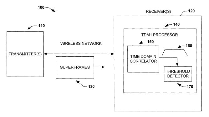
[0011] Fig. 1 is a schematic block diagram illustrating a time domain
correlator for
a wireless receiver.
[0012] Fig. 2 illustrates an example super frame structure.
[0013] Fig. 3 illustrates an example delayed correlator component for a
wireless
receiver.
[0014] Fig. 4 illustrates an example magnitude output for a time domain
correlator
detector.
[0015] Fig. 5 is illustrates an example state machine for time domain
multiplexing
pilot processing.
[0016] Figs. 6 and 7 are flow diagrams illustrating example processing for
time
domain multiplexing pilot signals.
[0017] Fig. 8 is a diagram illustrating an example user device for a wireless
system.
[0018] Fig. 9 is a diagram illustrating an example base station for a wireless
system.
[0019] Fig. 10 is a diagram illustrating an example transceiver for a wireless
system.
DETAILED DESCRIPTION
[0020] Systems and methods are provided for processing Time Domain
Multiplexing Pilot 1(TDM1) symbols via correlation in the time domain with the
delayed samples. In one embodiment, a method is provided for determining
synchronization information in an Orthogonal Frequency Division Multiplexing
(OFDM) broadcast. The method includes employing a time domain correlation to
detect the start of an OFDM super frame and utilizing the time correlation
operation to
correct the initial frequency offset between the transmitter frequency and the
local
receiver frequency. In one example, the sample can be employed in a forward
link only
system.
[0021] As used in this application, the terms "component," "network,"
"system,"
and the like are intended to refer to a computer-related entity, either
hardware, a
combination of hardware and software, software, or software in execution. For
example, a component may be, but is not limited to being, a process running on
a
processor, a processor, an object, an executable, a thread of execution, a
program,
and/or a computer. By way of illustration, both an application running on a
CA 02600487 2007-09-10
WO 2006/099527 PCT/US2006/009470
communications device and the device can be a component. One or more
components
may reside within a process and/or thread of execution and a component may be
localized on one computer and/or distributed between two or more computers.
Also,
these components can execute from various computer readable media having
various
data structures stored thereon. The components may communicate over local
and/or
remote processes such as in accordance with a signal having one or more data
paclcets
(e.g., data from one component interacting with another component in a local
system,
distributed system, and/or across a wired or wireless network such as the
Internet).
[0022] Fig. 1 illustrates time domain correlation for a wireless networlc
system 100
for determining timing synchronization and frequency offset. The system 100
includes
one or more transmitters 110 that communicate across a wireless network to one
or
more receivers 120. The receivers 120 can include substantially any type of
communicating device such as a cell phone, computer, personal assistant, hand
held or
laptop devices, and so forth. Portions of the receiver 120 are employed to
decode and
process a super frame 130 and other data such as multimedia data. The super
frame 130
is generally transmitted in an Orthogonal Frequency Division Multiplexing
(OFDM)
network that employs forward link only (FLO) protocols for multimedia data
transfer.
As illustrated, a Time Division Multiplexing Pilot 1 processor is provided to
process the
super frame and determine timing, and frequency offset. A time domain
correlator 150
receives the super frame 130 and generates a ramp output signal 160 when it
encounters
a TDMl OFDM symbol, where it is noted that TDM1 and TDM Pilotl are equivalent
terms.. From the ramp output 160, a threshold detector 170 employs a threshold
to
determine when a leading or trailing edge on the ramp has exceeded a
predetermined
threshold which can be programmed in the TDM1 processor 140, if desired. If
the
threshold has been exceeded for a predetermined time, a detection for TDM1 can
be
signaled and employed to synchronize operations of the receiver 120 with the
super
frame 130. Other aspects include detecting real and imaginary phase components
(e.g.,
I/Q) and sending to an automatic frequency control block (not shown).
[0023] Output from the time domain correlator 150 generates a well defined
ramp in
the time domain that can then be detected by comparing an edge of the ramp to
a
predetermined threshold in the detector 170. In one example, the TDM1
processor 140
provides a delay-and-correlate circuit 150, where the circuit correlates a
received
sample sequence with a sequence delayed by 128 samples. Since TDMl is periodic
and
CA 02600487 2007-09-10
WO 2006/099527 PCT/US2006/009470
6
each period is 128 samples, and since other OFDM symbols do not share this
characteristic, output of the detector 170 will have a significantly larger
magnitude
when TDM1 is present than when it is not present. In addition, the phase of
the time
domain correlator 150 output is proportional to the frequency offset between
the carrier
frequency of the received signal and the receiver 120 local oscillator
frequency. After
detection of the rising edge of the correlator output, it continues to check
the reliability
of the detection while observing for the end of TDM1 - the trailing edge of
the detector
output at 160. Data and further timing acquisition can then be based on
multiple
observations of the correlator output 160 when the output exceeds the
predetermined
threshold stored or programmed in the detector 170. In one embodiment, the
system
100 determines timing data in a wireless network. The system 100 includes
means for
analyzing a super frame (reference 150) to detect a signal magnitude in the
time domain
and means for detecting the signal magnitude (reference 170) to determine a
start timing
signal for the super frame 130. An automatic frequency loop (AFC) is updated
at the
end of detection of the TDM1 OFDM symbol by a value that is proportional to
the
phase of the correlator output.
[0024] Fig. 2 illustrates an example super frame structure 200. On initial
power-on,
after an automatic gain control (AGC) is settled, a modem acquires the frame
and coarse
OFDM symbol timing as well as frequency by processing a TDM Pilot 1 symbol
210.
In the time domain, TDM Pilot 1 at 210 consists of 36 periods of a sequence of
length
128. The structure of TDM Pilot 1 simplifies the implementation of the
correlator used
for its detection. The structure is also well suited for frequency estimation
in severe
multi-path channels as the waveform periodicity is preserved for the most
part. At 220,
TDM1 is shown as having 4096 sub-carriers in the frequency domain of which
only one
in thirty-two is non-zero, whereas at 230, TDM1 is broken into 128 samples in
the time
domain and then repeated 36 times.
[0025] Since the TDM Pilot 1 210 marks the beginning of each 1 second super
frame, the task of frame synchronization reduces to the detection of the TDM
Pilot 1
symbol. The time domain periodic structure of TDM Pilot 1 210 is exploited for
its
detection and estimation of coarse OFDM symbol timing. The TDM1 Pilot 1 symbol
210 is also used for the initial frequency estimation. The initial frame, time
and
frequency synchronization are achieved by processing the output of a delayed
CA 02600487 2007-09-10
WO 2006/099527 PCT/US2006/009470
7
correlation component as described in more detail below. The received signal,
with an
initial phase offset 0 and the frequency offset Af , is given by:
r(t) = x(t)ej (2YrAft+0) + n(t)
(1)
[0026] where x(t) is the TDM Pilot 1 signal. It is noted that x(t) = x(t+T),
where T
is the periodicity of TDM Pilot 1. The sampled version of the received signal
is:
r(kTs ) = x(kTs )e'(29AJxTs+0) + n(kTs )
(2)
[0027] where TS is the sampling period and k denotes the time index. If
rk = r(KTs ), Xk = x(KTS ), nk = n(KTs ), and Af = Of l fs (frequency error
normalized to sampling frequency), then:
rk = xkej2~7kAf-+O + nk
(3)
[0028] The following decision statistics are then formed:
k
Sk = rj riP =Zk +jZQ
j=k-(P-1)
(4)
[0029] where P is the period of TDM Pilot 1 in number of samples. The
acquisition
is based on the event that the magnitude of the correlator output exceeds a
predetermined threshold T which is described in more detail below.
[0030] Fig. 3 illustrates an example delayed correlator component 300. In
general,
timing and data acquisition can be based on multiple observations of the
correlator
output when it exceeds a threshold T 310. A sliding window integration over
the length
of 128 samples can be implemented by adding the newest term ( rk r~ 128 ) to
an
accumulator 320 and subtracting the oldest term ( rk-, 2sj,,zs6 ) from it at
330. Self-
correlating a periodic waveform of periodicity P can include an input buffer
of length P
at 340 to hold the last P input samples, and a single complex multiplier at
350. A shift
register or memory 360 of length P holds the last P product terms, wherein the
CA 02600487 2007-09-10
WO 2006/099527 PCT/US2006/009470
8
component at 330 provides a complex adder and a subtractor. A magnitude
squared
term is supplied to a threshold comparator at 310 to determine the presences
of TDM1
in the time domain. The magnitude of the delayed correlator output in a single
path
channel that has no noise when TDM Pilot 1 is present is shown in at 400 of
Fig. 4. The
delayed correlator output can be used for the detection of TDM Pilotl for
frame
synchronization and initial OFDM symbol timing estimation. The phase of the
correlator output can be used for the estimation of the initial frequency
offset.
[0031] Fig. 5 illustrates example implementation 500 of TDM Pilot 1
processing. A
samp_data_i/q and the 128-delayed del_samp_data i/q are input from an AFC
module
at 510. At each sampling clock, the samp_data value and the del_samp_data are
correlated as rjr*,_128 at 514. The output of the correlator (complex
multiplier) 514 is
stored in a Shift_register FIFO 520, which can be an SRAM with the size 128 x
12. The
correlator output 514 is also added 524 to a value stored in a
sum_correlated_data
accumulator 530 - moving window sum of 128 consecutive correlated outputs. In
the
same sampling clock interval, the 128-delayed correlator value read from the
Shift_register FIFO 520 is subtracted from the sum_correlated_data accumulator
at 524.
The Shift_register FIFO 520 is a circular buffer where a read pointer trails
the write
pointer by 128. The magnitude square of a "truncated" version of the
sum_correlated data at 534 is compared at 540 to a software-programmed
threshold
value at 544 in every sampling clock interval, with the result reported to a
TDM Pilotl
state machine 550. During a "flat-zone" of the TDM Pilotl detection as shown
in Fig. 4
at 400, the output of sum_correlated_data (I and Q) at 554 is written to an
sum
accumulator once every 128 sampling clocks. At the end of TDM1 detection, the
sum
accumulator value is written to the AFC block. The AFC block uses the tari
1(Q/I)
formula to calculate the frequency error between the TX clock and the local RX
clock.
[0032] An ARM Interface module 560 allows software to write to control
registers
that affect this block 500 and the AFC block. When TDM1 detection is reliable
and the
end of TDM1 is confirmed, the receiver assumes that the local clock has
approximately
synchronized to the carrier frequency after the AFC block has been updated.
Frame
synchronization is also achieved with high probability. A rough OFDM symbol
timing
estimate is determined based on the measurement of the falling edge of the
correlator
output during TDMl. The determined timing accuracy should be within a few
hundred
chips of the exact timing. The AFC block has two counters that determine the
timing.
An ofdm_symbol_counter tracks the OFDM symbol number in the Superframe. The
CA 02600487 2007-09-10
WO 2006/099527 PCT/US2006/009470
9
falling edge of the TDM Pilotl correlator output is marlced as OFDM symbol
'1', with
TDM Pilotl being considered as OFDM symbol '0'. It is noted that the falling
edge of
the correlator output occurs in the symbol after the TDM Pilotl OFDM symbol.
The
second counter in AFC, intra_ofdm_counter, tracks the sample number in the
OFDM
symbol. The intra_ofdm_counter is initialized with a value of (256-17) on the
detection
of the falling edge of the correlator output. At this point, the receiver is
ready to
demodulate WIC and LIC symbols and then process the TDM Pilot2 (also referred
to as
TDM2) to acquire fine time synchronization.
[0033] The ARM interface module 560 implements software registers that control
the TDM Pilotl and AFC blocks. The TDM Pilotl FSM implements the state machine
responsible for detecting the TDM Pilotl. The receiver determines the local-
and wide-
area networks in which it is operating from the WOI and LOI ID symbols
following the
TDMl. The information is used to set up the correct scrambling sequences to
properly
descramble the data symbols. TDM2 is periodic and each period is 2048 chips.
According to the rough timing estimate determined based on TDM1, a fine timing
deterrnination block operates on a segment of 2048 samples of TDM2 to generate
an
estimate of the time-domain transmission channel. The channel estimate of
length 2048
is generated from the 2048 chips of TDM2 and it is circularly shifted by the
amount
equal to the rough timing error. If the span of the true channel is less than
1024 chips,
the receiver can uniquely determine the delay and profile of the channel. The
initial
accurate timing (i.e., the position of the FFT window) can be derived from the
profile
and the delay of the channel estimate.
[0034] In general, the initial acquisition procedure based on the doing the
correlation of the TDM1 symbol has three stages. It is to be appreciated that
the
following example hard-coded numbers in the following description are for
illustration
of an example embodiment. In one implementation of these embodiments, these
numbers are programmable via software. During the first stage, an algorithm
searches
for the leading edge of the correlation curve. The magnitude square of the
correlator
output is compared with programmable threshold T at 540. If the correlator
output
exceeds the threshold consecutively for 64 input samples (or other determined
amount),
the algorithm enters the second stage of the acquisition process.
[0035] In the second stage, a hit count at 564 is incremented each time the
magnitude square of the correlator output exceeds the threshold at 540. The
algorithm
can return to the first stage if it determines that the leading edge observed
was false.
CA 02600487 2007-09-10
WO 2006/099527 PCT/US2006/009470
This is indicated by the correlator output remaining below the threshold for
greater than
or equal to 128 input samples and the hit count being less than 400.
[0036] The algorithm remains in the second stage for at least 34 periods or
until it
observes a consistent trailing edge of the correlation curve. The algorithm
leaves the
second stage (a consistent trailing edge is found) when the correlator output
remains
below the threshold for 768 input samples and the hit count is greater than or
equal to
400. The algorithm also exits the flat zone if it has stayed for at least 4352
samples (34
* 128).
[0037] The accumulator sum of the correlator output is updated once every 128
samples during the second stage. If the trailing edge was not observed in the
second
stage, the observation continues during the third stage. In the third stage,
if the
correlator output remains below the threshold for a minimum of 32 consecutive
input
samples and if the correlator output exceeded the threshold for at least 2000
input
samples during the second stage, TDM1 detection is declared. The AFC loop is
updated
with the value of the accumulator sum. The phase value of the accumulator sum,
which
is proportional to the frequency offset is used to correct the frequency error
between the
transmitter and the receiver.
[0038] The initial OFDM symbol time estimate is based on the trailing edge of
the
waveform depicted in Fig. 4. The time instance when the correlator output
transitions
below the threshold for the last time during observation of the trailing edge
is taken as
the 239th (256-17) sample of the next OFDM symbol (TDM pilot 2). If the hit
count at
560 is found to be less than 2000 or a consistent trailing edge during a time-
out period
of 1024 input sample in stage 3 is not observed, the algorithm resets the
counts and
returns to the first stage to observe another leading edge. The sum
accumulator of the
correlator is not sent to the AFC block and sum accumulator is reset.
[0039] The programmable threshold T 444 can depend on the AGC setting and is
recommended to be computed as T = (1/4) (128* 6S2)2 where 652 is the received
signal
power. Since the AGC provides a constant signal plus noise power M = 6SZ +
6n2, 0 0
dB Signal-to-Noise Ratio (SNR) can be used for a given operating M to compute
the
threshold T. For ADC range 1, the full-scale power can be 2. If a significant
AGC
error is expected (in fast fading), it should be considered when computing the
threshold.
The threshold should be computed for a negative AGC error that favors high SNR
operation; otherwise, the detection performance at a high SNR may degrade.
CA 02600487 2007-09-10
WO 2006/099527 PCT/US2006/009470
11
[0040] Due to gain sensitivity variation, the data collection for initial
frequency
acquisition is done when the correlator output is above the threshold with a
frequency
error detector based on the periodic structure of TDM1 and a large loop
bandwidth.
After the leading edge detection is declared, data acquisition for the initial
frequency
acquisition occurs during the flat zone (or second stage) of the acquisition
procedure.
The sum accumulator of the correlator is updated once every 128 input samples.
Although the algorithm can stay in the second stage for 34 or more periods,
the number
of updates to the sum accumulator of the correlator is limited to 28. Because
channels
may have excess delay spread, the tail end of the TDM1 symbol is not typically
periodic. As a result, the frequency estimate based on the tail end of the
flat zone may
not be reliable. The frequency offset is calculated by taking the arctan of
the sum
accumulator of the correlator.
[0041] Figs. 6 and 7 illustrate example processes 600 and 700 for time domain
multiplexing pilot signals. While, for purposes of simplicity of explanation,
the
methodologies are shown and described as a series or number of acts, it is to
be
understood and appreciated that the processes described herein are not limited
by the
order of acts, as some acts may occur in different orders and/or concurrently
with other
acts from that shown and described herein. For example, those skilled in the
art will
understand and appreciate that a methodology could alternatively be
represented as a
series of interrelated states or events, such as in a state diagram. Moreover,
not all
illustrated acts may be required to implement a methodology in accordance with
the
subject methodologies disclosed herein.
[0042] The processes 600 and 700 depicted in Figs. 6 and 7 relate to the state
machine described above with respect to Fig. 5. In general, the state machine
is in
IDLE state at 610 until it is enabled by software and all memory locations in
a
corr_mem (Shift Register FIFO) have been written with '0's. The next state,
START_RIS EDGE_DETECT at 620, is the starting point to detect the rising edge
of
the comparator. In this state, a run_count counter is held in reset state. If
the
comparator output is '1', implying that the sum-correlator value is greater
than the
threshold, the state machine transitions to the RIS_EDGE_ON state at 630. At
every
sampling clock edge, the run_count counter is incremented by 1 if the
comparator
output is '1'. If the comparator is '0' on any sampling clock edge, the state
machine
goes from the RIS_EDGE_ON state 630 to the START_RIS_EDGE_DETECT state
620 and the process starts over again. When the run_count reaches 64, implying
that for
CA 02600487 2007-09-10
WO 2006/099527 PCT/US2006/009470
12
64 consecutive samples the correlator output is '1', the state machine goes to
the
START_FLAT_REGION state at 640, resetting counters interval_count, hit_count,
and
run_count.
[0043] The interval_count counter is incremented on every sampling clock edge
and
tracks the number of samples elapsed; the hit_count counter tracks the number
of
sampling clocks for which the comparator output is '1' (i.e., comparator
output is above
threshold); the run_count counter tracks the number of sampling clocks in
succession
for which the comparator is V. From the START_FLAT_REGION 640, the state
machine transitions to FLAT_ABOVE_THRESHOLD 650 if the comparator is '1' or to
FLAT_BELOW_THRESHOLD 660 if the comparator is V. The state machine moves
between the two states 650 and 660 depending on the value of the comparator at
every
sampling clock edge. In the FLAT_ABOVE_THRESHOLD state 650, if the
interval_count is greater than sw_ic_flat (i.e., stayed long enough) and the
comparator
output is '0', the state machine proceeds to START FALL EDGE_DETECT state.
From the FLAT_BELOW_THRESHOLD state 660, the next state is also
START_FALL_EDGE_DETECT 670 based on any of the three conditions shown in
Fig. 6.
[0044] The condition ((run_count >= sw_rc_false_rise) AND (hit_count <
sw_hc_false_rise)) relates to the false rising edge detection in the output of
the
comparator. The condition ((run_count >= sw_rc_fall) AND (hit_count >=
sw_hc_fall))
relates to seeing a consistent falling edge and can be either true or false
detection. The
condition ((interval_count >= sw_ic_flat) and (run_count > 0)) ensures that
the state
machine does not get stuck in this state if no falling edge is detected. In
the
START_FALL_EDGE_DETECT state 670, the interval_count is reset. If the
hit_count
is less than sw_hc_flat, the state machine proceeds to START_RIS_EDGE_DETECT
620 and the process starts over again, as it implies that the correlator
output was not
above threshold for a sufficient time. Otherwise: If the comparator output is
'1' the
state machine goes to FALL_ABOVE_THRESHOLD 650. Then, if the interval_count
equals sw_ic_after fall, which implies that the expected "fall" is not
occurring, the state
machine goes to START_RIS_EDGE_DETECT 620. If the comparator output is '0',
the state machine goes to FALL_BELOW_THRESHOLD 660. Then, if the
interval_count exceeds sw_ic_after fall or if the run_count exceeds
sw_rc_after fall,
the state machine proceeds to TDM PILOTI DET state which is shown at 710 of
Fig.
7 (i.e., TDM Pilotl has been detected successfully).
CA 02600487 2007-09-10
WO 2006/099527 PCT/US2006/009470
13
[0045] Fig. 8 is an illustration of a user device 800 that is employed in a
wireless
communication environment, in accordance with one or more aspects set forth
herein.
User device 800 comprises a receiver 802 that receives a signal from, for
instance, a
receive antenna (not shown), and performs typical actions thereon (e.g.,
filters,
amplifies, down converts, etc.) the received signal and digitizes the
conditioned signal
to obtain samples. Receiver 802 can be a non-linear receiver. A demodulator
804 can
demodulate and provide received pilot symbols to a processor 806 for channel
estimation. A FLO channel component 810 is provided to process FLO signals.
This
can include digital stream processing and/or positioning location calculations
among
other processes. Processor 806 can be a processor dedicated to analyzing
information
received by receiver 802 and/or generating information for transmission by a
transmitter
816, a processor that controls one or more components of user device 800,
and/or a
processor that both analyzes information received by receiver 802, generates
information for transmission by transmitter 816, and controls one or more
components
of user device 800. A memory may also be provided to facilitate processor
execution.
It is noted that the device 800 is exemplary in nature and intended to convey
general
functionality. With respect to forward link only (FLO) functionality, the FLO
stream
can co-exist with a wireless device such as a phone but is essentially
independent of
normal device transmit and receive operations. Hence, a FLO channel would not
employ the transmitter 816.
[0046] It will be appreciated that the data store (e.g., memories) components
described herein can be either volatile memory or nonvolatile memory, or can
include
both volatile and nonvolatile memory. By way of illustration, and not
limitation,
nonvolatile memory can include read only memory (ROM), programmable ROM
(PROM), electrically programmable ROM (EPROM), electrically erasable ROM
(EEPROM), or flash memory. Volatile memory can include random access memory
(RAM), which acts as external cache memory. By way of illustration and not
limitation, RAM is available in many forms such as synchronous RAM (SRAM),
dynamic RAM (DRAM), synchronous DRAM (SDRAM), double data rate SDRAM
(DDR SDRAM), enhanced SDRAM (ESDRAM), Synchlink DRAM (SLDRAM), and
direct Rambus RAM (DRRAM). The memory 808 of the subject systems and methods
is intended to comprise, without being limited to, these and any other
suitable types of
memory. User device 800 further comprises a background monitor 814 for
processing
CA 02600487 2007-09-10
WO 2006/099527 PCT/US2006/009470
14
FLO data, a symbol modulator 814 and a transmitter 816 that transmits the
modulated
signal.
[0047] Fig. 9 is an illustrates an example system 900 that comprises a base
station 902 with a receiver 910 that receives signal(s) from one or more user
devices
904 through a plurality of receive antennas 906, and a transmitter 924 that
transmits to
the one or more user devices 904 through a transmit antenna 908. Receiver 910
can
receive information from receive antennas 906 and is operatively associated
with a
demodulator 912 that demodulates received information. Demodulated symbols are
analyzed by a processor 914 that is similar to the processor, and which is
coupled to a
memory 916 that stores information related to user ranks, lookup tables
related thereto,
and/or any other suitable information related to performing the various
actions and
functions set forth herein. Processor 914 is further coupled to a FLO channel
918
component that facilitates sending FLO information to one or more respective
user
devices 904. A modulator 922 can multiplex a signal for transmission by a
transmitter
924 through transmit antenna 908 to user devices 904.
[0048] Fig. 10 shows an exemplary wireless communication system 1000. The
wireless communication system 1000 depicts one base station and one terminal
for sake
of brevity. However, it is to be appreciated that the system can include more
than one
base station and/or more than one terminal, wherein additional base stations
and/or
terininals can be substantially similar or different for the exemplary base
station and
terminal described below.
[0049] Referring now to Fig. 10, on a downlink, at access point 1005, a
transmit
(TX) data processor 1010 receives, formats, codes, interleaves, and modulates
(or
symbol maps) traffic data and provides modulation symbols ("data symbols"). A
symbol modulator 1015 receives and processes the data symbols and pilot
symbols and
provides a stream of symbols. A symbol modulator 1020 multiplexes data and
pilot
symbols and provides them to a transmitter unit (TMTR) 1020. Each transmit
symbol
may be a data symbol, a pilot symbol, or a signal value of zero. The pilot
symbols may
be sent continuously in each symbol period. The pilot symbols can be frequency
division multiplexed (FDM), orthogonal frequency division multiplexed (OFDM),
time
division multiplexed (TDM), frequency division multiplexed (FDM), or code
division
multiplexed (CDM).
[0050] TMTR 1020 receives and converts the stream of symbols into one or
more analog signals and further conditions (e.g., amplifies, filters, and
frequency up
CA 02600487 2007-09-10
WO 2006/099527 PCT/US2006/009470
converts) the analog signals to generate a downlink signal suitable for
transmission over
the wireless channel. The downlink signal is then transmitted through an
antenna 1025
to the terminals. At terminal 1030, an antenna 1035 receives the downlink
signal and
provides a received signal to a receiver unit (RCVR) 1040. Receiver unit 1040
conditions (e.g., filters, amplifies, and frequency down converts) the
received signal and
digitizes the conditioned signal to obtain samples. A symbol demodulator 1045
demodulates and provides received pilot symbols to a processor 1050 for
channel
estimation. Symbol demodulator 1045 further receives a frequency response
estimate
for the downlink from processor 1050, performs data demodulation on the
received data
symbols to obtain data symbol estimates (which are estimates of the
transmitted data
symbols), and provides the data symbol estimates to an RX data processor 1055,
which
demodulates (i.e., symbol de-maps), de-interleaves, and decodes the data
symbol
estimates to recover the transmitted traffic data. The processing by symbol
demodulator
1045 and RX data processor 1055 is complementary to the processing by syinbol
modulator 1015 and TX data processor 1010, respectively, at access point 1005.
[0051] Processors 1090 and 1050 direct (e.g., control, coordinate, manage,
etc.)
operation at access point 1005 and terininal 1030, respectively. Respective
processors
1090 and 1050 can be associated with memory units (not shown) that store
program
codes and data. Processors 1090 and 1050 can also perform computations to
derive
frequency and impulse response estimates for the uplink and downlink,
respectively.
[0052] Systems and devices described herein may be implemented in hardware,
software, or a combination thereof. For a hardware implementation, the
processing
units used for channel estimation may be implemented within one or more
application
specific integrated circuits (ASICs), digital signal processors (DSPs),
digital signal
processing devices (DSPDs), programmable logic devices (PLDs), field
programmable
gate arrays (FPGAs), processors, controllers, micro-controllers,
microprocessors, other
electronic units designed to perform the functions described herein, or a
combination
thereof. With software, implementation can be through modules (e.g.,
procedures,
functions, and so on) that perform the functions described herein. The
software codes
may be stored in memory unit and executed by the processors 1090 and 1050.
[0053] For a software implementation, the techniques described herein may be
implemented with modules (e.g., procedures, functions, and so on) that perform
the
functions described herein. The software codes may be stored in memory units
and
executed by processors. The memory unit may be implemented within the
processor or
CA 02600487 2007-09-10
WO 2006/099527 PCT/US2006/009470
16
external to the processor, in which case it can be communicatively coupled to
the
processor via various means as is known in the art.
[0054] What has been described above includes exemplary embodiments. it is, of
course, not possible to describe every conceivable combination of components
or
methodologies for purposes of describing the embodiments, but one of ordinary
skill in
the art may recognize that many further combinations and permutations are
possible.
Accordingly, these embodiments are intended to embrace all such alterations,
modifications and variations that fall within the spirit and scope of the
appended claims.
Furthermore, to the extent that the term "includes" is used in either the
detailed
description or the claims, such term is intended to be inclusive in a manner
similar to
the term "comprising" as "comprising" is interpreted when employed as a
transitional
word in a claim.