Note: Descriptions are shown in the official language in which they were submitted.
CA 02600804 2010-12-10
76186-150
WIRELESS COMMUNICATION PORT
Field of The Invention
[0002] The field of the invention is wireless adapters.
Background Of The Invention
[0003] Several serial to Ethernet converters are known, including for
example the X-PortTM from LantronixTM, aspects of which were described in
U.S. Patent No. 6,881,096 issued April 19, 2005. A more recent example
includes
the CP/ComTM converter available from Arc ElectronicsTM. (www.arcelect.com).
[0004] The earliest Ethernet converters did not provide wireless
connectivity. Subsequent converters, including PCMCIA cards and USB dongles,
do provide wireless connectivity, but such devices are not designed for
surface
installation on computer or other circuit boards. In addition, the existing
converters are designed for particular translations of one protocol to another
or
they have limited or non-existing MILARRS and other functionality. PCMCIA
cards, for example, are designed to require a complex parallel interface
(e.g. CARDBUS) not typically provided on non-computer products or devices.
Existing wireless connectivity devices are therefore not generally suitable to
OEM
manufacturers for use in their products.
[0005] Thus, there is an ongoing need to provide an electronic component
board mountable modules that provide wireless connectivity, especially those
that
use a simple serial interface to the component board. There is also an ongoing
need to provide modules that provide web server and other more advanced
functionality.
Summary Of The Invention
[0006] The present invention provides methods and apparatus in which a
module has: an electronic component board mountable housing that includes a
logic circuitry that translates
-1-
CA 02600804 2007-09-04
WO 2006/099627 PCT/US2006/010061
between a serial communication protocol and a wireless communication protocol;
a physical
connector for connection to the board; and a connector to an antenna.
[0007] The housing can comprise any suitable size and shape, an especially
contemplated
embodiment of which has a cross-section of a typical RJ45 connector. Other
contemplated
embodiments are flatter and wider, with an especially preferred embodiment
having a
substantially square horizontal cross-section, and a height about 20% of the
length or width.
Pins are the currently preferred connectors for electrical coupling to the
board, and the
module can be connected to the board either directly or through an
intermediate connector
piece. As used herein, the term "mounted on the board" contemplates both types
of situations,
direct and indirect mounting. Pins can be soldered to form a permanent
connection if desired.
Any suitable number of pins can be used, from 2 or 3 through 7, 8, or 9, and
even more.
[0008] The circuitry is preferably disposed on a single chip, although it can
be split among
multiple components. Preferred modules contain flash or other high speed RAM,
at least 256
K13 to store an operating system, and at least 2 MB of additional memory to
store firmware,
web pages, and so forth. Preferred modules can advantageously include a
voltage
supervisory circuit that uses a power feed of no more than 5 Volts DC,
although higher and
lower power feeds are contemplated as required by the circuitry. Currently,
the most
preferred voltage is 3.3 V.
[0009] Modules are preferably general purpose, being designed to accommodate
any serial
communication protocol. This includes especially 12C, CAN, ProfiBus, SPI, and
USB.
Similarly, modules are preferably designed to handle any suitable serial and
management
standards, including for example, IP, ARP, UDP, TCP, ICMP, Telnet, TFTP,
AutolP, DHCP,
HTTP, and SNMP. It is especially contemplated that modules will comply with
any of the
802.11 x or superseding standards.
[0010] Commercial embodiments preferably include software that provide
functionality other
than simply protocol translation and wireless networking support. For example,
the software
can advantageously provide a security function such as WEP (Wired Equivalent
Protocol)
and WPA (Wireless Networking Protected Access) security, and various types of
encryption.
Software can also provide at least one of a MILARRS functionality. In other
examples, the
software can provide web related services such as email alert.
-2-
CA 02600804 2011-09-07
76186-150
[0011] An antenna can be fixedly or detachably coupled to the antenna
connector, and can be mounted at the module, or external to the module using a
coaxial or other suitable cable. Multiple antennas are also contemplated.
[0012] The novel modules can be used wherever a device designer wants a
plug-in (or "drop-in") system that obviates the need for independent design,
development and maintenance of wireless capability. Examples include servers,
desktop and laptop computers, and even devices such as kitchen appliances with
relatively simpler electronics. It is especially contemplated that the novel
modules
can be used on devices having one or more rigid or flexible component boards,
and
can be implemented with more than one such module on a given board to provide
redundancy, or to provide intra- or inter- board communication.
[0012a] According to one aspect of the present invention, there is provided a
module comprising: an electronic component board mountable housing that
includes
a logic circuitry that translates between a serial communication protocol and
a
wireless communication protocol; a physical connector for connection to a
major
surface of an electronic component board; and an RJ45 connector and an
antenna,
each of which is electronically coupled to the logic circuitry.
[0013] Various objects, features, aspects and advantages of the present
invention will become more apparent from the following detailed description of
preferred embodiments of the invention, along with the accompanying drawings
in
which like numerals represent like components.
Brief Description Of The Drawings
[0014] Figure 1 is a front perspective view of a PCB board mountable
converter module that uses a wired Ethernet connection.
[0015] Figure 2 is a front view of the module of Figure 1.
3
CA 02600804 2011-09-07
76186-150
[0016] Figure 3 is a side, partially cut-away view of the module of Figure 1.
[0017] Figure 4 is a side cross-sectional view of the module of Figure 1.
[0018] Figure 5 is a block diagram of the electrical component circuitry for
the
module of Figure 1.
[0019] Figure 6 is a pin input and output diagram of the module of Figure 1,
or
a wireless embodiment.
[0020] Figure 7 is a side, partially cut-away view of an alternative
embodiment
of a module, having horizontal and angles circuit boards.
3a
CA 02600804 2007-09-04
WO 2006/099627 PCT/US2006/010061
[0021] Figure 8 is a side, partially cut-away view of an alternative
embodiment of a module,
having circuit boards placed on a common flexible substrate.
[0022] Figure 9 is a side, partially cut-away view of an alternative
embodiment of a module,
having vertical and angled circuit boards.
[0023] Figure 10 is an alternative embodiment of a connector, having an
interior chamber
located beneath the connector port.
[0024] Figure 1 IA is a perspective cutaway view of a commercial WiPortTM
module.
[0025] Figure 11B is a bottom perspective view of a commercial WiPortTM
module.
[0026] Figure 12 is a perspective cutaway view of a module in which a serial
to wireless
Ethernet capability is embodied in a housing having an approximate cross-
sectional size and
shape of an RJ-45 connector.
[0027] Figure 13 is a cutaway view of a device having a board having two
wireless modules.
Detailed Description Of The Invention
[0028] In Figures 1, 2 and 3, module 10 comprises a generally rectangular
housing 12. The
front of the housing includes an open cavity 14. A metal Faraday shield covers
the top, sides
and back of the housing and provides for electromagnetic-radiation (EMR)
protection. The
module 10 additionally includes spring biased grounding tabs 16 that connect
the Faraday
shield to chassis (earth) ground by contacting the enclosure in which the
connector is
mounted. Also shown is an array of leads 20 for electrically interconnecting
the module 10
to a printed circuit board (PCB) 18.
[0029] The cavity 14 of the housing 12 incorporates a planar array of parallel
electrical
contacts 22 to provide the necessary electrical contacts to form a connector
port within the
cavity 14. The cavity 14 is sized and dimensioned and the contacts 22 are
placed within the
cavity to compliment a mating plug (not shown). The sized cavity 14 along with
the contacts
22 form a standard RJ-45 connector jack. The jack contacts 22 are spring
biased for
engagement with a mating plug (not shown). An important advantage is that
novel modules
as set forth herein can attach a conventional RJ-45 jack with magnetics,
because the Ethernet
wires are brought out of the multipin connector.
-4-
CA 02600804 2007-09-04
WO 2006/099627 PCT/US2006/010061
[0030] The housing 12 is fornied of molded plastic or other suitable material
used in the art,
covered by a Faraday shield having a front wall 24, a rear wall 26, a top wall
28, a bottom
wall 30, and sidewalls 32 and 34. The references herein to "top", "bottom",
and "sides" are
made for ease of explanation relative to the drawing. Alternative embodiments
eliminate the
plastic, and the housing material is chosen to perform the Faraday shielding
function without
separate components, for example by using conductive metal. It is also
contemplated that the
module 10 can be oriented in a multitude of ways on a product, thereby
accommodating
engineering requirements of specific placements.
[0031] The front wall 24 includes LEDs 36 and 38. The LEDs provide visual
status and fault
information for various functions of the serial-to-Ethernet conversion, such
as (but not
limited to) Ethernet connection speed, link present/absent, full/half duplex,
Ethernet activity,
serial port activity, and microcontroller error conditions.
[0032] In Figures 3 and 4 the housing 12 includes a segregated interior
chamber 40. A first
PCB 42 is disposed within the interior chamber 40 generally horizontal and
parallel relative
to the bottom wall 30. The first PCB 42 is soldered (or otherwise electrically
connected) to
the contact interface 44, which is mounted in a plastic insert. The completed
insert assembly
slides and snaps into the main housing 12. The contact interface pins 44 are
formed such that
their ends become the wiper contacts 22. Thus, the first PCB 42 is
electrically interconnected
to the contacts 22 of the port cavity 14. The contact interface 44
additionally provides
structural support to the first PCB 42.
[0033] A second PCB 50 is also placed within the interior chamber 40,
positioned generally
horizontal and in general parallel relation to the bottom wall 30. The third
PCB 50 is
soldered (or otherwise electrically connected) to the array of leads 54, which
are formed such
that their ends become the input/output pins 20 (more specifically, these pins
20 connect
power and ground, reset, serial data input and output, handshake and flow
control lines, and
PIO lines) that connect to the user's PCB 20. The array of leads 54 are
mounted in a plastic
insert. After the third PCB 50 is soldered (or otherwise connected) to the
leads 54, the
completed insert assembly slides and snaps into the main housing 12.
[0034] A third PCB 48 is placed within the interior chamber 40 in a generally
vertical
orientation, and is generally perpendicular to the other PCBs 42 and 50. PCB
48 is
positioned adjacent the rear wall 26 and is structurally and electrically
interconnected to the
-5-
CA 02600804 2007-09-04
WO 2006/099627 PCT/US2006/010061
other PCBs 42 and 50 by the formed pins 49 and 52. PCB 48 and formed pins 49
and 52 thus
provide the electrical connection between PCBs 42 and 50. The LEDs 38 have
leads (not
shown) that run close to the top of the enclosure 12, and these leads also
connect to holes in
PCB 48. This provides the electrical connection between the LEDs 38 and the
control PCB
50.
[0035] The first, 42, and second PCB 50 collectively incorporate the
electronic circuitry
component necessary to complete a serial-to-Ethernet conversion of data. PCB
42 includes
the magnetics portion of the circuitry which can advantageously include
isolation
transformers, common mode chokes, termination resistors, and a high voltage
discharge
capacitor (for ESD and voltage surges). In this implementation, PCB 48 is used
solely for
electrical interconnection, but it could also be used for circuitry components
if required.
[0036] PCB 50 incorporates all of the electronic circuitry components
necessary for the
control function of the serial-to-Ethernet conversion. The electronic
components on board
PCB 50 include, but are not limited to, a microprocessor and an Ethernet
controller (which
can advantageously be combined in an ASIC), nonvolatile memory (flash memory
in the
present invention), voltage regulator, voltage supervisory circuit, crystals,
resistors,
capacitors, and ferrite or other surface mount beads.
[0037] In operation, the complete assembly is mounted on a PCB that is a part
of some
device or equipment. Serial data and general purpose PIO data flows from the
device through
the array of leads 20 and is processed by the circuitry collectively
incorporated onto PCBs 42,
48 and 50. PCB 42 is interconnected to the contacts 22 which mate with a plug
(not shown)
to effectively transmit Ethernet data thereto. Ethernet data can also flow
from the Ethernet
port through wiper contacts 22, be processed by the circuitry collectively
incorporated onto
PCBs 42, 48 and 50, and flow out as serial data and general purpose PIO data
through lead
pins 20 into the external device. It is additionally contemplated that the
control circuitry,
magnetic circuitry and LED circuitry can be interchanged among PCBs 42, 48 and
50 and
that component can be positioned on one or both sides of each PCB's 42, 48 and
50.
[0038] In Figure 5 the controller block 56 handles all of the conversion
between serial and
Ethernet. This includes processing of the digital (serial) and analog
(Ethernet) signals, as
well as all of the required code protocol translations. The controller block
56 communicates
with Ethernet through the Ethernet interface 58, which is described below in
greater detail.
-6-
CA 02600804 2011-09-07
76186-150
The flash memory 60 stores the software that the controller block 56 uses to
perform its
functions. The supervisory circuit 68 monitors the supply voltage corning in
through the
PCB 10 pins 64. It resets the controller block if the voltage drops too low,
or if a signal from
the PCB 10 pins 64 requests a system reset. The power filters 61 remove noise
from the
input supply voltage, and also reduce any noise that might be transmitted from
the serial-to-
Ethernet converter to the outside world through the voltage supply lines. The
power supply
62 supplies one or more voltages required by the controller block. Serial data
is transmitted
to and from the controller block through the PCB IO pins .64 to the external
device. The flow
control and handshake lines (connected through PCB IO pins 64) are standard
signals used to
control the serial data stream. The controller block can also communicate with
the external
device through the PIO lines connecting through the PCB IO pins 64. It is
understood that
although the components as shown in Figure 5 are specifically identified, all
suitable control
circuitry that implement the desired functions are also contemplated.
[0039] In Figure 6 the outgoing Ethernet signal 70a from the controller 50
passes through
the isolation transformer 74, which eliminates any DC coupling problems
between Ethernet
devices. The outgoing signals pass through the common mode choke 78, which
reduces
spurious emissions (radiated and conducted). The outgoing signal connects to
the Ethernet
cable through contacts 72a of the RJ-45 jack. Incoming Ethernet signals enter
into the jack
through contacts 72c, and pass through a common mode choke 80 that reduces
spurious
common mode noise that could be conducted into the device. The signals pass
through the
isolation transformer 76, and then to the controller board 50 through pins 52
and 26. The
center taps 70b and 70c of the isolation transformers 74 and 76 are used to
set the appropriate
DC bias levels in the transmit and receive circuitry on the controller board
50. These center
taps also connect to the controller board 50 through pins 52 and 26. Four of
the RJ-45
contacts 72c are not used for Ethernet signals. They are terminated to ground,
through
matching resistors 82c and 82d and capacitor 84, to reduce noise and DC
transients. DC
transients ("ESD") on the Ethernet cable that are present at the contact 72a
and 72c are
reduced by discharge to ground through resistors 82a and 82b.
[0040] The alternate module of Figure 7 is structurally similar to the
embodiment shown in
Figures 1-4, with only the distinctions highlighted below. Within the interior
chamber 40a,
two PCBs 86 and 88 are positioned therein. A first PCB 88 is positioned
generally horizontal
in parallel relation to the bottom wall 30a. A second PCB 86 is positioned in
angular relation
-7-
CA 02600804 2007-09-04
WO 2006/099627 PCT/US2006/010061
to the PCB 88 to fit within the interior chamber 40a. PCB 86 and 88
collectively incorporate
the electric circuitry components to complete a serial to Ethernet data
conversion. PCB 86 is
interconnected to a lead array 20a. PCB 86 includes all of the control
circuitry, with
components interconnected to the top side and bottom side of said PCB. PCB 86
is
interconnected to PCB 88. PCB 88 includes the magnetic portion of the
circuitry formed on
the underside of PCB 86. The LEDs 38a and 36a (not shown) also connect to PCB
86
through leads 14a. PCB 88 is interconnected to contacts 22a.
[0041] The alternate module of Figure 8 is also structurally similar to the
embodiment as
shown in Figures 1-4. However, here a common flexible substrate (more
specifically, a
rigid/flexible PCB 90, 92, 94, and 96) is formed to fit the interior chamber
40b. The
rigid/flexible PCB 90, 92, 94, and 96 collectively incorporates the electric
circuitry
components to complete a serial to Ethernet data conversion. Electrical and
magnetic
components can be mounted on the rigid portions of the PCB 92, 94, and 96.
Electrical
connections between the rigid portions 92, 94, and 96 are made on the flexible
portions 90.
Rigid portion 96 is electrically connected to the lead array 20b. Control
circuitry can be
incorporated onto rigid portion 96 and possibly 94, with magnetic circuitry
incorporated on
rigid portion 92 and possibly 94. The LEDs connect to rigid portion 96 through
leads 14b.
Rigid portion 92 is electrically connected to contacts 22. It is additionally
contemplated that
the control circuitry, magnetic circuitry and LED connections can be
interchanged among
rigid portions 92, 94 and 96.
[0042] The alternate module of Figure 9 is again structurally similar to the
embodiment
shown in Figures 1-4. The main difference is that two PCBs 98 and 100 are
positioned
within the interior chamber 40c. The first PCB 98 is positioned generally
vertically in
parallel relation to the rear wall 26. A second PCB 100 is positioned in
angular relation to
the PCB 98 to fit within the interior chamber 40c. PCB 98 and 100 collectively
incorporate
the electric circuitry components to complete a serial-to-Ethernet data
conversion. PCB 100
is interconnected to a lead array 20c. PCB 100 includes all of the control
circuitry with
components interconnected to the top side and bottom side of said PCB. PCB 98
is
interconnected to PCB 100. PCB 98 includes a magnetic portion of the
circuitry. PCB 98 is
interconnected to contacts 22c. PCB 100 is additionally interconnected to LEDs
38c and 36c.
-8-
CA 02600804 2011-09-07
76186-150
[00431 The alternate module of Figure 10 once again includes a connector port
that is
structurally similar to the embodiment shown in Figures 1-4, but which does
not include an
interior chamber located behind the port. In the alternate embodiment shown in
Figure 10,
the interior chamber 102 is located beneath the port cavity 14d. Within the
interior chamber
102, at least one PCB is positioned therein which incorporates the electric
circuitry
components to complete a serial-to-Ethernet data conversion. It is
contemplated by the
present invention that the serial-to-Ethernet circuitry can be incorporated
into the interior
chamber 102 in a variety of ways, including those described with respect to
the interior
chambers of Figures 4 and 7-9. It is further contemplated that the port cavity
14d in any
embodiment can be replaced or augmented with a radio antenna, radio antenna
connector or
remote radio antenna wiring.
[00441 Wireless networking versions of the modules of Figures 1-10 can be
implemented by
replacing the magnetics with a suitable radio circuitry and power amplifier,
receiver, etc.
Such substitutions can be implemented without altering the overall design of
the module, but
is more preferably implemented using structure and electronics as set forth in
Figures 1lA-C,
12 and 13.
[00451 The modules of Figures 11A and 11B differ from the embodiment shown in
Figures
1-4 with major distinctions being the addition of Ethernet radio
functionality, which replaces
or augments all or a portion of Ethernet magnetic circuitry previously
described with respect
to PCB boards 42 and 50.
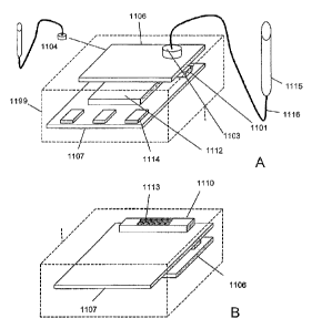
[0046] While the partitioning of required circuitry on the interior PCBs
within the interior
chamber can be accomplished in any suitable manner, it is especially
convenient to arrange
the Ethernet radio components on a single PCB 1106, with remaining control and
supervision
circuitry on PCB 1107. The board or boards can be positioned in any practical
relationship
with respect to each other and with respect to the housing 1199. The first PCB
1 106 includes
antenna connector 1103 and can advantageously provide for a second (diversity)
antenna or
connector 1104. The second PCB 1 107 can alternatively replace leads 54 by
including
mating connector 1101 for electrical board mounting.
[0047] Connector 1 101 comprises three or more pins 11.13 and can include any
or all of serial
data pins, handshaking and flow control pins, GPIO pins and pins supporting
other serial or
parallel protocols as desired. PCB 1107 can also incorporate all of the
electronic circuitry
-9-
CA 02600804 2007-09-04
WO 2006/099627 PCT/US2006/010061
components necessary for the control function of the serial-to-Ethernet
conversion. There
are, of course, a great diversity of pins in use, and additional pin
configurations will
undoubtedly be utilized in the future. With that caveat in mind, connector
1101 is to be
interpreted euphemistically to include all manner of pin cross sections,
square, rectangular,
flattened, etc, and all manner of configurations of pins. An important
advantage is that novel
wireless modules as set forth herein may attach a conventional RJ-45 jack
incorporating
magnetics, because the Ethernet wires maybe brought out of connector 1101. By
including
appropriate programming, data communication may take place between and among
any of
the provided interfaces and protocols, including serial, wireless and wired
Ethernet interfaces.
[0048] The electronic components on PCB 1107 can include, but are not limited
to, a micro-
processor and an Ethernet controller (combined in an ASIC for the present
invention), at least
256KB of memory that stores an operating system and environment and at least
2MB of
nonvolatile memory that stores at least one web page (flash memory in the
present invention),
voltage regulator, voltage supervisory circuit, crystals, resistors,
capacitors, and ferrite beads
(surface mount beads in the present invention).
A current commercial embodiment according to Figures 11A and 11B has the
following
specifications:
Wireless Specifications
Network Standard IEEE 802.11b
Frequency Range 2.412 - 2.484 GHz
Output Power l4dBm +/- 1.0 dBm
Antenna Connector 1, no diversity supported.
Radio # of Selectable 14 Chamiels
Channels
Modulation DSSS, DBPSK, DQPSK, CCK
Antenna 1
Connector
Security WEP 64/128, TKIP
Maximum Receive Level -1OdBm (with PER < 8%)
= -82dBm for 11Mbps
Receiver Sensitivity = -87dBm for 5.5Mbps
= -89dBm for 2.0Mbps
= -93dBm for 1.0Mbps
WLAN Power and Link Max: 4mA
LED Current
Other Specifications
-10-
CA 02600804 2007-09-04
WO 2006/099627 PCT/US2006/010061
CPU, Memory Lantronix DSTni-EX 186 CPU, 256 KB zero wait state SRAM
2048 KB Flash or 4096 KB Flash, 16 KB Boot ROM, 1024 KB
SRAM
Firmware Upgradeable via TFTP and serial port
Reset Circuit Reset In is low active. Minimum reset pulse width is 2 ms at HL
_ -500 A
Serial Interface CMOS (Asynchronous) 3.3V-level signals
Rate is software selectable (300 bps to 921600 bps)
Serial Line Formats 7 or 8 data bits, 1-2 Stop bits,
Parity: odd, even, none
Modem Control DTR, DCD
Flow Control XON/XOFF (software), CTS/RTS (hardware), none
Network Interface Wireless 802.1lb and 10/100 Ethernet
Protocols Supported 802.11b, ARP, UDP, TCP, Telnet, ICMP, SNMP, DHCP,
BOOTP, Auto IP, HTTP, SMTP, TFTP
Data Rates With = 11Mbps
Automatic Fallback = 5.5Mbps
= 2Mbps
= 1Mbps
Media Access Control CSMAICA with ACK
Frequency Range 2.412 - 2.484 GHz
Range Up to 328 feet indoors
Modulation Techniques = CCK (11Mbps)
= CCK (5.5 Mbps)
= DQPSK (2 Mbps)
= DBPSK (1 Mbps)
Transmit Output Power 14dBr ldBm
Average Power = 1280 mW (WLAN mode; maximum data rate)
Consumption = 820 mW (WLAN mode; idle)
= 710 mW (Ethernet mode)
Peak Supply Current 460 mA
Management Internal web server, SNMP (read only)
Serial login, Telnet login, Devicelnstaller software
Security Password protection, locking features, 64/128 bit WEP
Internal Web Server Serves web pages
Storage capacity: 1.8 MB or 3.8 MB (depending on Flash size)
Weight 29 grams
Material Metal shell
Temperature Operating range, WLAN: -40 C to +70 C
Operating range, Ethernet: -10 C to +75 C
-11-
CA 02600804 2011-09-07
76186-150
Storage range: -40 C to +85 C (-40 F to 185 F)
Included Software WindowsTM 98/NT/2000/XP based Devicelnstaller configuration
software and WindowsTM based Comm Port Redirector,
Devicelnstaller, Web-Manager.
[0049] The microprocessor can advantageously implement MILARRS functionality.
MILARRS refers to the following: Monitoring the state of the device for an
administrator;
Inventory the devices sub-systems, components, or assets; Logging data or
events generated
by the device; Alerting an administrator of device state or taking action
based on defined
rules; Recovering the device if it fails or shuts down; Reporting device
information or
diagnostics to an administrator; and Securing the device and its assets from
threats and risks.
Additional details regarding the acronym and implementation are set forth in
U.S. Patent
No. 7,698,405 issued April 13, 2010.
[0050] In Figure 12, the housing 1201 can represent a similar form factor in
height and width
to conventional passive RJ45 jacks, where height can be in a range of 12 to 14
mm or more
and width in a range of 15 to 24mm or more. In a particularly preferred
embodiment, height
is approximately 13 mm and width is approximately 16mm. The translation
circuitry can be
split among multiple components disposed on PCB 1203 and PCB 1204, or even
across other
boards as can be necessary or desirable. In addition to antenna 1205 a second
(diversity)
antenna can be provided.
[0051] In Figure 13, a device 1301 has one or more component boards 1304,
1305, upon
which are mounted two modules 1303 and 1306. The 1303 module is directly
connected to
the board 1304 using soldered pins. The 1306 module can be mounted on the
board 1305
using an intermediate coupling. The modules 1303 and 1306 are able to.talk
with one
another and with a device 1302 in the outside world wirelessly using their
respective antenna
1307, 1312 and 1308 via the conventional device to device paths 1309 and 1310
but also by
the unconventional path 1311 connecting two points within the same device
wirelessly. Path
1311 can be desirable for providing routing flexibility, architectural
generality, and digital
signal integrity including secure encryption or physical convenience.
[0052] The device of Figure 13 is drawn generically, and is intended to
represent any suitable
device, including but not limited to Information Technology equipment,
electronic
communications equipment, networked device appliances or remote management
modules,
medical or security equipment, industrial monitoring, sensing or control
equipment, digital
-12-
CA 02600804 2007-09-04
WO 2006/099627 PCT/US2006/010061
storage or processing devices and equipment and consumer audio or video
entertainment
components or devices. Such contemplated devices vary tremendously, and for
example, can
range in size from chip scale components to rack mounted enclosures to room or
building
sized systems, and in intelligence from basic GPIO signal communication to
complete
protocol bridging functions or inclusion of management functions such as
provision of one or
all of MILARRS functions, web services, gateway functions, database access or
search, or
any other function enabled by wireless local or worldwide network connection.
[0053] Thus, specific embodiments and applications of wireless communication
ports have
been disclosed. It should be apparent, however, to those skilled in the art
that many more
modifications besides those already described are possible without departing
from the
inventive concepts herein. The inventive subject matter, therefore, is not to
be restricted
except in the spirit of the appended claims. Moreover, in interpreting both
the specification
and the claims, all terms should be interpreted in the broadest possible
manner consistent
with the context. In particular, the terms "comprises" and "comprising" should
be interpreted
as referring to elements, components, or steps in a non-exclusive manner,
indicating that the
referenced elements, components, or steps can be present, or utilized, or
combined with other
elements, components, or steps that are not expressly referenced.
-13-