Note: Descriptions are shown in the official language in which they were submitted.
CA 02601021 2007-09-10
WO 2006/095257 PCT/IB2006/000531
1
"MICROARRAY DEVICE FOR DNA RECOGNITION, APPARATUS USING THE
MICROARRAY DEVICE, AND CORRESPONDING METHOD OF OPERATION '
TECHNICAL FIELD
The present invention relates to a microarray device for DNA
recognition, to an apparatus for analysis using the microarray
device, and to the corresponding method of operation.
BACKGROUND ART
In current methods for fast DNA recognition, use is known of
so-called DNA-microarrays, which are constituted by
microfabricated devices, which enable the need of being able
to perform a multiplicity of simultaneous analyses on a DNA
specimen to be met in such a way as to supply in relatively
short times the results of said analyses.
DNA microarrays currently in use, referred to hereinafter as
"hybridization microarrays", are made up of a solid support
constituted by a thin layer of glass, silicon, quartz, or
other appropriate material, made on which is a plurality of
"detection sites or cells" of microscopic dimensions, referred
to hereinafter as "microlocations", each of which is
associated to a pre-set DNA sequence.
In particular, the pre-set DNA sequence present in each of the
microlocations of the hybridization microarray is constituted
by a specific non-hybridized single-helix DNA probe typically
immobilized on the surface of the solid support.
During the process of DNA recognition, following upon the step
of polymerase-chain-reaction (PCR) amplification and
dissociation of the two DNA helices of the sample material,
the latter is set in contact with the microlocations in such a
way as to enable the DNA probes of the microlocations
themselves to hybridize or not with the individual
complementary DNA helices of the specimen to be examined.
CA 02601021 2007-09-10
WO 2006/095257 PCT/IB2006/000531
2
It should be specified that the term "hybridization" is meant
to indicate a known biochemical process, whereby a pre-set DNA
probe "binds" in a highly specific and selective way to the
DNA to be examined, in the case where in the latter a sequence
complementary to the pre-set probe itself is present.
Figure 1 illustrates, in an extremely schematic way, some of
the operations implemented by a method of DNA recognition
using a hybridization microarray which is prevalently in use
today.
Initially, the recognition method implements an operation I of
"marking" the individual DNA helices of the sample material to
be analysed. In detail, the DNA helices are marked with labels
of fluorescent material typically referred to as "optical
markers".
Following upon the marking step, the sample material is set in
contact with the microlocations present on the hybridization
microarray to carry out an operation II of hybridization. In
this step, all the microlocations of the hybridization
microarray come into contact with the specimen of material to
be analysed itself, the DNA sequences of which hybridize only
with the complementary DNA probes immobilized on the
microlocations.
In particular, on the microlocations in which the
hybridization has occurred, a certain number of fluorescent
markers present on the DNA specimen is immobilized, whilst the
remaining "free" sequences present in solution, which have not
undergone hybridization, are removed from the hybridization
microarray so as to enable optical reading of the fluorescent
markers immobilized on the microlocations themselves.
At this point, with the use of a microscope, an operation III
CA 02601021 2007-09-10
WO 2006/095257 PCT/IB2006/000531
3
of optical acquisition is performed of the two-dimensional
image of the surface of the hybridization microarray on which
the fluorescent markers that have remained immobilized in a
position corresponding to the microlocations may be seen.
The image acquired is then supplied by the microscope to a
processing unit, which, using a specific program for image
processing, identifies the various fluorescent markers present
on the hybridization microarray and, on the basis of the
latter, performs DNA recognition of the specimen analysed.
The method of DNA recognition using the hybridization
microarray described above presents various drawbacks.
In the first place, the operation of marking the individual
helices of DNA of the material is an extremely critical stage
of the method described above in so far as it can cause a
contamination of the material to be examined, consequently
introducing errors in the process of DNA recognition.
In addition, the method requires the use of extremely
sophisticated and complex programs of image processing, and
can currently be implemented only using different types of
independent tools that are non-homogeneous with respect to one
another (for example, microscopes, personal computers, etc.),
which, in addition to being costly, depend heavily upon human
intervention, consequently affecting the times required for
analysis.
Finally,.the method described above not only does not enable
real-time DNA recognition, but does not even enable analyses
to be performed with a sufficient degree of accuracy, it being
consequently inadequate for carrying out analyses of a
quantitative type.
CA 02601021 2007-09-10
WO 2006/095257 PCT/IB2006/000531
4
DISCLOSURE OF INVENTION
The aim of the present invention is consequently to provide a
microarray device that will be able to overcome the drawbacks
described above.
According to the present invention, a microarray device for
DNA recognition is provided as indicated in Claim 1 and,
preferably, in any one of the subsequent claims depending
either directly or indirectly upon Claim 1.
According to the present invention, an apparatus for DNA
recognition which uses a microarray device is moreover
provided, as indicated in Claim 14.
Finally, according to the present invention a method for DNA
recognition through a microarray device is provided, as
indicated in Claim 19.
BRIEF DESCRIPTION OF THE DRAWINGS
The present invention will now be described with reference to
the annexed plate of drawings, which illustrate a non-limiting
example of embodiment thereof, and in which:
- Figure 1 is a schematic illustration of a series of
operating steps implemented in a method for DNA recognition
via a hybridization microarray built according to the known
art;
- Figure 2 is a schematic perspective view, with parts removed
for reasons of clarity, of a microarray device made according
to the teachings of the present invention;
- Figures 3 to 8 are schematic illustrations of respective
embodiments of the microarray device built according to the
teachings of the present invention;
- Figure 9 is a schematic illustration of an optical-
amplification device comprised in the microarray device
illustrated in Figure 1;
- Figure 10 shows the time evolution of the threshold voltage
in a memory cell, when the latter is impinged upon by a beam
CA 02601021 2007-09-10
WO 2006/095257 PCT/IB2006/000531
of ultraviolet radiation;
- Figure 11 is a schematic illustration of an apparatus for
DNA recognition built according to the teachings of the
present invention; whilst
5 - Figure 12 is a schematic illustration of the method for DNA
recognition provided according to the teachings of the present
invention.
BEST MODE FOR CARRYING OUT THE INVENTION
The present invention is essentially based upon the principle
of emitting, after the step of hybridization of the DNA, one
or more beams of ultraviolet radiation towards the
microlocations present on the hybridization microarray, and
detecting via a detection microarray that is integrated or can
be suitably coupled to the hybridization microarray, the
absorption of ultraviolet radiation by each microlocation when
the latter is traversed by the beam of ultraviolet radiation.
In other words, the present invention is essentially based on
the idea of measuring the difference of absorption of
ultraviolet radiation by the DNA of a material (or fragments
thereof) according to whether the latter is or not in a state
of hybridization, i.e., whether it is present in the form of a
single or double helix.
It should be pointed out that said difference of absorption of
ultraviolet radiation, which will be referred to hereinafter
as "differential absorption", may occur as final effect of two
different processes of hybridization. In the case in point, a
first process gives rise to the so-called "hypochromic
effect", by virtue of which hybridization of the DNA, given
the same amount of material, causes a reduction of the
absorption of ultraviolet radiation (approximately 30%). It is
evident then that, in this case, the identification of the
microlocations that have a reduced absorption of radiation
renders possible discrimination of the. hybridized DNA
CA 02601021 2007-09-10
WO 2006/095257 PCT/IB2006/000531
6
sequences from the non-hybridized ones.
The second process, instead, which is independent of the
hypochromic effect and is of more general application, occurs
when the hybridization takes place with DNA probes immobilized
in a microlocation. In this case, following upon hybridization
the solution to be analysed by the hybridization microarray is
removed, and remaining in the microlocations in which the
hybridization has occurred is material in excess that
comprises the hybridized DNA that has remained "anchored" to
the complementary DNA probe. Said excess of material in the
hybridized microlocations causes an increase of the absorption
of ultraviolet radiation in areas corresponding to the
microlocations themselves with respect to the absorption that
occurs in the microlocations where hybridization has not
occurred. It is evident then, that in this case, by
identifying the microlocations that have a greater absorption
of radiation, it is possible to discriminate the hybridized
DNA sequences from the non-hybridized ones.
With reference to Figures 2 to 8, number 1 designates as a
whole a microarray device, which basically comprises a
hybridization microarray 2 provided with a plurality of
microcells or microlocations 3, each associated to a specific
DNA sequence; and a detection microarray 4, which is
appropriately coupled to the hybridization microarray 2 and is
provided with a plurality of microsensors 5 of ultraviolet
radiation, each of which is designed to supply an electrical
signal SM corresponding to the absorption of ultraviolet
radiation by a corresponding microlocation 3 present in the
hybridization microarray 2.
In the example illustrated in Figure 2, the hybridization
microarray 2 is provided with a preferably, but not
necessarily, plane solid support, which can be made of at
least one thin layer of glass, silicon, quartz, plastic or any
CA 02601021 2007-09-10
WO 2006/095257 PCT/IB2006/000531
7
other similar material typically used in the techniques of
microfabrication of electronic chips.
The microlocations 3 are positioned on the outer surface 2a of
the solid support, which is designed in use (as will be
described in detail hereinafter) to be impinged upon by a beam
of ultraviolet radiation, referred to hereinafter for reasons
of brevity with the term "UV radiation". It should be pointed
out that the UV beam can present a spectrum of radiation
having a pre-set wavelength comprised substantially between
200 and 400 nm.
With reference to the example illustrated in Figure 2, in
particular the microlocations 3 are distributed on the outer
top surface 2a with an appropriate density, (which can for
example be of the order of hundreds, thousands, or hundreds of
thousands of microlocations per square centimetre) preferably
according to a geometrical matrix or grid configuration, in
which each microlocation 3 is associated to a given row-column
combination of the array.
As regards the detection microarray 4, it is provided with a
solid, preferably plane, support, which can be made of a layer
of glass, silicon, quartz, or any other similar material
typically used in the techniques of microfabrication of
electronic chips, and is designed to be coupled to the solid
layer of the hybridization microarray 2 on the side opposite
to the surface 2a impinged upon in use by the UV radiation, in
such a way as to present each microsensor 5 aligned with the
corresponding microlocation 3 of the hybridization microarray
2 in a direction corresponding to the optical path followed by
the UV radiation.
In the example illustrated in Figure 2 in particular, the
microsensors 5 are aligned with the respective microlocations
3 in a vertical direction, in such a way as to be able to
CA 02601021 2007-09-10
WO 2006/095257 PCT/IB2006/000531
8
receive each only the portion of the beam of ultraviolet
radiation that traverses the respective microlocation 3 so as
to be able to measure the absorption of UV radiation that
occurs in the microlocation 3 itself.
The microsensors 5 are arranged on the solid support of the
detection microarray 4 preferably according to a geometrical
matrix or grid configuration altogether equivalent to the
geometrical matrix configuration presented by the
microlocations 3 on the surface 2a of the hybridization
microarray 2 in such a way that each microsensor 5 will be
perfectly aligned to the corresponding microlocation 3 and
associated to a given row-column combination of its own array.
With reference to the example illustrated in Figures 3, 4 and
5, the microarray device 1 further comprises, preferably but
not necessarily, a reading microdevice 8, which has the
function of co-ordinating the "electrical" detection of the
electrical signals SM generated by the microsensors 5 present
in the detection microarray 4, to supply the electrical
signals SM themselves to a processing unit described in detail
hereinafter, which has the function of processing the
electrical signal SM to supply the indication regarding the
DNA of the material examined.
In particular, the reading microdevice 8 is able to co-
ordinate reading of the electrical signals SM generated by the
microsensors 5 via an appropriate system of row-column
addressing, which enables unique identification of each
microsensor 5 on the corresponding array so as to be able co-
ordinate reading of the absorption of the UV radiation in each
point in a selective way.
The reading microdevice 8 is moreover able to treat, i.e.,
condition or amplify appropriately the electrical signals SM
that it receives from the microsensors 5 of the detection
microarray 4, to be able to supply them at output according to
CA 02601021 2007-09-10
WO 2006/095257 PCT/IB2006/000531
9
a pre-set electrical format so as to enable the processing
unit to receive and read the electrical signals SM.
In the example illustrated in Figures 3, 4 and 5, the reading
microdevice 8 is provided with a solid, preferably plane,
support, which can be made with a thin layer of glass,
silicon, quartz, or any other similar material typically used
in the techniques of microfabrication of electronic chips,
within which one or more electronic microcircuits 8a are
integrated, which are designed to be electrically connected to
the microsensors 5 in order to receive at input the electrical
signals SM produced by the latter, and are able to perform the
different functions of addressing of the microsensors 5, and
of treatment of the electrical signals SM during acquisition
of the latter by a processing unit.
In the example illustrated in Figure 3, the hybridization
microarray 2, the detection microarray 4, and the reading
microdevice 8, which make up the microarray device 1, are
integrated with one another in such a way as to provide a
monolithic chip, in which the detection microarray 4 is stably
fixed to the hybridization microarray 2, and the reading
microdevice 8 is in turn stably fixed to the detection
microarray 4. In the case in point, the integration can
envisage, for example, that the hybridization microarray 2,
the detection microarray 4, and the reading microdevice 8 are
made "in layers" with technologies typical of microfabrication
or integrated circuits.
It is evident that the hybridization microarray 2, the
detection microarray 4, and the reading microdevice 8 that
make up the microarray device 1 can be completely separate
from one another or integrated in pairs according to different
possible combinations.
For example, according to an embodiment illustrated in Figure
CA 02601021 2007-09-10
WO 2006/095257 PCT/IB2006/000531
4, the detection microarray 4 and the reading microdevice 8
are integrated with one another in such a way as to form a
single monolithic chip, whilst the hybridization microarray 2
is separate and independent therefrom and is designed, in use,
5 to be coupled to the detection microarray 4.
It is evident that in this case the coupling between the
hybridization microarray 2 and the detection microarray 4 can
be obtained, for example, by setting the solid support of the
10 hybridization microarray 2 directly resting on the top surface
of the solid support of the detection microarray 4 in such a
way as to provide a vertical alignment between the
microsensors 5 of the detection microarray 4 and the
corresponding microlocations 3 of the hybridization microarray
2.
In the case in point, following upon the aforementioned
alignment, each microsensor 5 of the detection microarray 4 is
set immediately underneath a corresponding microlocation 3 in
such a way as to be able to detect the portion of the beam of
ultraviolet radiation that traverses the microlocation 3
itself.
According to a different embodiment illustrated in the example
of Figure 5, the detection microarray 4 and the hybridization
microarray 2 are integrated with one another in such a way as
to form a single monolithic chip, whilst the reading
microdevice 8 is separate and independent therefrom and is
designed, in use, to be coupled to the detection microarray 4
in such a way as to be able to receive at input the electrical
signals SM.
With reference to Figure 6, each microlocation 3 of the
hybridization microarray 2 is defined by a microsump of
capillary dimensions, which is made on the top surface 2a of
the layer of the hybridization microarray 2 and is designed to
CA 02601021 2007-09-10
WO 2006/095257 PCT/IB2006/000531
11
contain inside it a solution containing in turn one or more
specific DNA probes. In the case in point, the solution
containing the DNA probe or probes can be constituted by a
liquid solution and/or a"dry ' solution.
According to a different embodiment illustrated schematically
in Figures 7 and 8, each microlocation 3 of the hybridization
microarray 2 comprises a pre-set plurality of DNA probes that
are identical to one another (numbering four in Figures 7 and
8), each of which is immobilized appropriately on the top
surface 2a of the hybridization microarray 2.
Each specific DNA probe, designated by the number 3a,
comprises a plurality of monomolecular layers deposited on the
surface 2a of the solid support via an appropriate
intermediate linker layer in the "immobilized" form. In the
case in point, the pre-set DNA probes are "immobilized" in the
microlocations 3 by means of known techniques, which use a
series of layers of different material for creating suitable
bonds, for example of a multiple type between a substrate and
an intermediate (linker) layer, and between the latter and
each pre-set DNA probe. In greater detail, the location of the
pre-set DNA probes on each specific microlocation 3 can be
obtained both with precise positioning systems, for example
using the technology of precision ink-jet printers, and by
means of successive "maskings", as in traditional lithographic
techniques.
Conveniently, in one of the possible embodiments described
above (Figure 5), in which the hybridization microarray 2 and
the detection microarray 4 are made together "in layers"
according to technologies typical of microfabrication, the
surface 2a of the hybridization microarray 2, on which the
pre-set DNA probes are immobilized, may also be constituted by
means of an outer passivation of a chip.
CA 02601021 2007-09-10
WO 2006/095257 PCT/IB2006/000531
12
With reference to Figure 8, the hybridization microarray 2
further comprises preferably, but not necessarily, an optical-
amplification device 9, which has the function of causing the
UV beam to interact a number of times with the DNA probes 3a
containing the monomolecular layers in such a way as to bring
about an increase in the differential absorption of
ultraviolet radiation by the DNA probes in the case where
hybridization of the DNA with the probes themselves occurs.
In particular, the optical-amplification device 9 can comprise
a series of reflecting and/or half-reflecting mirrors,
designed to perform the operations of reflection and hence of
amplification of the UV beam towards the DNA probes present in
the microlocations 3.
In the example illustrated schematically in Figure 8, the
optical-amplification device 9 comprises a plurality of half-
reflecting mirror microelements, which are arranged in pairs
in a position corresponding to each microlocation 3. In the
case in point, each pair of mirror microelements associated to
a microlocation 3 comprises a first mirror microelement
designated by 9a, which is set on top of, and facing, the
microlocation 3, and a second mirror microelement designated
by 9b, which is set immediately underneath the microlocation
3. The mirror microelements 9a and 9b are preferably half-
reflecting in such a way as to be able to be traversed by the
UV beam and at the same time partially reflect the UV
radiation towards the DNA probes of the microlocation 3.
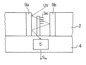
According to a variant illustrated in Figure 9, in each
microlocation 3, the first and the second mirror microelements
9a, 9b are completely reflecting and are arranged in positions
parallel to one another in such a way as to cause the UV beam
to interact a number of times in a direction substantially
transverse to the DNA probes 3a present in the microlocation 3
and having the same DNA sequence so as to determine an
CA 02601021 2007-09-10
WO 2006/095257 PCT/IB2006/000531
13
amplification of the differential absorption on the DNA
sequences.
It should be pointed out that, in this case, the UV beam is
emitted in a direction substantially transverse to the surface
plane of at least one of the two mirror microelements 9a, 9b,
which reflect to one another the radiation in such a way as to
impinge upon the DNA probes and "convey" the radiation itself
towards the microsensor 5.
As regards, instead, the microsensors 5 of the detection
microarray 4, they can be made up preferably, but not
necessarily, of storage devices, such as, for example, non-
volatile memory cells (not illustrated).
It is known in fact that the memory cells, following upon
programming thereof (corresponding to the operation of
writing) remain in a stable condition, in which they have a
pre-set voltage threshold, typically high, and that the
"erasure" of the information contained in the memory cell, is
performed by irradiating the cell itself with a UV beam.
During irradiation of the memory cell with the UV radiation,
the voltage threshold of the memory cell decreases
progressively as a function of the quantity of UV radiation
received. Indicated by way of example in Figure 10 is a
typical time evolution of the value of the voltage threshold
of a memory cell as a function of the exposure of the memory
cell itself to UV radiation.
It is evident then that the memory cell supplies at output an
electrical signal that has a voltage proportional to the
quantity of UV radiation that impinges upon the cell itself,
performing in this specific case the same function as a UV
sensor.
CA 02601021 2007-09-10
WO 2006/095257 PCT/IB2006/000531
14
In particular, each memory cell used in the specific case as
microsensor 5 of UV radiation present in the detection
microarray 4 can be preferably, but not necessarily, made
according to CMOS technology. In the case in point, each
microsensor 5 can be formed by a memory cell of an EPROM or
EEPROM type made preferably in the "single poly level" form.
The memory cells that make up the microsensors 5 described
above are known and consequently will not be described further
herein.
With reference to Figure 11, an apparatus 10 for DNA
recognition using at least one microarray device 1 described
above is illustrated.
In the example illustrated in Figure 11, in addition to the
microarray device 1 described above, the apparatus 10
comprises preferably, but not necessarily, a source 11 of UV
radiation, which can be constituted, for example, by a UV-
laser emitter device, or by a UV lamp, or by any other similar
type of apparatus designed to emit a UV beam in the direction
of the outer surface 2a of the microarray device 1 in such a
way as to illuminate the array of the microlocations 3.
The apparatus 10 further comprises a processing unit 12, which
is designed to receive and process the electrical signals SM
generated by the microsensors 5 following upon illumination of
the microlocations 3, in such a way as to supply, on the basis
of said processing, a set of information regarding DNA
recognition of the material analysed.
In the case in point, the processing unit 12 is able to
process the electrical signals SM generated by the
microsensors 5 to identify the microlocations 3, i.e.,. the
specific DNA probes, which during the process of hybridization
have "bound" to the complementary sequences of the DNA
analysed, hence distinguishing them from the microlocations 3,
CA 02601021 2007-09-10
WO 2006/095257 PCT/IB2006/000531
i.e., from the DNA probes that have remained "free".
From the foregoing description, it should be pointed out that
the processing implemented by the processing unit 12 is
5 essentially based upon differential absorption (described
previously), by virtue of which it is possible to distinguish
the microlocations 3 on which the hybridization by the other
microlocations 3 has occurred, analysing the absorption of UV
radiation by them.
Consequently, the processing unit 12 calculates, according to
each electrical signal SM, the absorption of UV radiation that
occurs in each microlocation 3, and according to said
absorption is able to establish whether hybridization of the
corresponding DNA probe has occurred or not in the
microlocation 3 itself.
Once identified and discriminated, the hybridized
microlocations 3 from the "non-hybridized" microlocations 3,
the processing unit has available all the information
sufficient for complete DNA recognition.
On the basis of the foregoing description, it should be added
that the apparatus 10, in addition to carrying out DNA
recognition, is able to perform advantageously an analysis of
a quantitative type on the DNA specimen in such a way as to
determine the effective "concentration" of DNA in the material
examined.
Said concentration can in fact be detected by emitting the UV
beam in the direction of a hybridization microarray 2, in
which the microlocations 3 comprise a plurality of DNA probes
that have one and the same DNA sequence but have a pre-set
differentiated DNA concentration.
In this case, the pre-set concentrations of DNA present in the
CA 02601021 2007-09-10
WO 2006/095257 PCT/IB2006/000531
16
DNA probes present in the microlocations 3 determine,
following upon hybridization with the complementary probes of
the material analysed, different absorptions of UV radiation,
on the basis of which it is possible to identify and hence
discriminate the DNA probes that have hybridized with
complementary probes having a concentration' of DNA greater
than a certain threshold from the DNA probes that have
hybridized with complementary probes having a concentration of
DNA lower than the threshold itself.
It is therefore evident that in this case the processing unit
12 of the apparatus 10 calculates, according to each
electrical signal SM, the absorption of UV radiation that
occurs in each microlocation 3, and, according to said
absorption, is able to determine the concentration of DNA
present in the material examined.
The processing unit 12 can comprise: an electronic circuit
provided with an interface module 13 that is able to manage
acquisition and the reading of the electrical signals SM
generated and supplied by the microsensors 5 through the
reading microdevice 8; and a computation module 14,
constituted, for example, by a microprocessor, which processes
each signal SM to detect the absorptions of the microlocations
3, so as to identify the hybridized microlocations 3.
From the foregoing description, it should be pointed out that
the electrical coupling and/or connection between the
microarray device 1 and the interface module 13 can be made in
different ways according to the embodiment of the microarray
device 1.
The microarray device 1 and/or each of its components
described above, in particular the reading microdevice 8,
according to the embodiment can in fact be fixed and
electrically connected in a removable or fixed way to the
CA 02601021 2007-09-10
WO 2006/095257 PCT/IB2006/000531
17
interface module 13.
The processing unit 12 may further comprise preferably, but
not necessarily, a control module 15, which is able to drive
the source 11 appropriately during emission of the UV beam,
and a display device 16 for example a monitor or a display
able to display the information regarding DNA recognition.
From what has been set forth above, it should be pointed out
that the method of DNA recognition using the microarray device
1 described above, which can be implemented by the apparatus
10 of analysis, comprises the steps described in what follows.
With reference to Figure 12, following upon the step of
hybridization (dashed block designated by 100) between a
specimen of the material to be examined and the specific DNA
probes present in the microlocations 3 of the microarray
device 1, activation of the source 11 that emits a UV beam
towards the surface 2a of the microarray device 1 is
controlled in such a way as to irradiate the microlocations 3.
In this step, the UV radiation generated by the source 11
follows a pre-set optical path that traverses the surface 2a
in such a way as to impinge upon each microlocation 3. It is
evident that, should the microarray device 1 be provided with
the optical-amplification device 9 (arrangement indicated in
Figure 6), the UV radiation, following upon traversing of the
surface 2a, is reflected partially by the mirror elements 9a
and 9b, causing a controlled amplification of the differential
absorption on each microlocation 3.
Each microsensor 5 of the detection microarray 4 detects the
UV radiation absorbed by the corresponding microlocation 3, to
supply at output the electrical signal SM indicating the
absorption of UV radiation by the microlocation 3 itself
(dashed block designated by 110).
CA 02601021 2007-09-10
WO 2006/095257 PCT/IB2006/000531
18
At this point, the reading microdevice 8 of the microarray
device 1 co-ordinates acquisition of the electrical signals
SM, to supply them at input to the processing unit 12, which
processes them to recognize the DNA of the specimen of the
material being analysed (dashed block designated by 120). In
particular, in this step the processing unit 12 calculates
according to the electrical signals SM the differential
absorption that has occurred in each microlocation 3 and, on
the basis of the latter, discriminates the microlocations 3
containing the specific DNA probes affected by hybridization
from the microlocations 3 containing the specific non-
hybridized DNA probes.
Once the discrimination is completed, the processing unit 12
is able to supply, through the display device 16, the
indications regarding DNA recognition of the material
examined.
It should be added that, in the case where the microlocations
3 of the hybridization microarray contain specific DNA probes
having the same DNA sequence but a differentiated
concentration, the processing unit 12 is able to determine, as
a function of the differential absorption that has occurred in
each microlocation 3, the concentration of DNA of the material
being analysed (associated to the known DNA sequence).
The method of DNA recognition using the microarray device 1
described above affords the major advantage of not requiring
any process of marking of the material to be analysed with
fluorescent optical markers, thus eliminating completely any
possibility of contamination of the material itself prior to
its analysis.
The microarray device 1 described above moreover presents
potentially very low production costs and consequently leads
CA 02601021 2007-09-10
WO 2006/095257 PCT/IB2006/000531
19
to a considerable reduction in the costs involved in DNA
recognition. For example, in the embodiment described above,
where the separation of the hybridization microarray 2 from
the remaining components is envisaged, the hybridization
microarray can be of the disposable type.
In the case in point, as already anticipated, the
hybridization microarray 2 can be each time set resting on the
detection microarray 4, thus enabling the microsensors 5 to
measure the UV radiation absorbed by the microlocations 3.
Finally, the microarray device 1 could advantageously be
integrated in a multifunctional structure that comprises
elements for control and handling of the DNA specimen, such as
for example an integrated system of microfluidic channels for
movement of the specimen in solution and its passage according
to a correct dynamics in the area corresponding to the
microlocations, or else an integrated system of temperature
control for optimization of the reaction of molecular
recognition in terms of specificity and efficiency. Said
control could be implemented so as to be able to act both
locally and globally in regard to the device. Said integration
of the microarray device 1 in one of the systems mentioned
above in fact enables a greater facility of use for.the user,
increases the portability of the system of analysis, and
finally improves the performance thanks to a greater control
of the physico-chemical parameters of the reaction of
recognition between receptors and target molecular species.
Finally, as regards the apparatus 10, in addition to not
requiring high computing powers in so far as the method
described above eliminates the need to perform image
processing, performs DNA recognition in "real time" and
affords the possibility of detections also of a quantitative
type.
CA 02601021 2007-09-10
WO 2006/095257 PCT/IB2006/000531
Finally, it is clear that modifications and variations can be
made to the microarray device 1, to the apparatus 10, and to
the method of DNA recognition described and illustrated
herein, without thereby departing from the scope of the
5 present invention, defined by the annexed claims.