Note: Descriptions are shown in the official language in which they were submitted.
CA 02601130 2007-09-13
1
DESCRIPTION
THREE-AXIS MAGNETIC SENSOR AND METHOD FOR
MANUFACTURING THE SAME
TECHNICAL FIELD
[0001]
The present invention relates to a three-axis magnetic sensor provided with an
X-axis sensor to which a plurality of magnetoresistive effect elements are
bridge-connected, a Y-axis sensor to which a plurality of magnetoresistive
effect
elements are bridge-connected and a Z-axis sensor to which a plurality of
magnetoresistive effect elements are bridge-connected within one substrate,
and also
relates to a method for manufacturing the three-axis magnetic sensor.
Priority is claimed on:
Japanese Patent Application No. 2005-77010 filed March 17, 2005;
Japanese Patent Application No. 2005-90581 filed March 28, 2005;
Japanese Patent Application No. 2005-91256 filed March 28, 2005;
Japanese Patent Application No. 2006-32124 filed February 9, 2006; and
Japanese Patent Application No. 2006-32125 filed February 9, 2006, the
contents of
which are incorporated herein by reference.
BACKGROUND ART
[0002]
Giant magnetoresistive elements (GMR elements), tunneling magnetoresistive
elements (TMR elements) and the like are known as elements usable in a
magnetic sensor.
CA 02601130 2007-09-13
2
These magnetoresistive effect elements are provided with a pinned layer in
which the
magnetization direction is pinned (bonded) in a predetermined direction and a
free layer
in which the magnetization direction changes according to an external magnetic
field,
indicating as an output a resistance value according to the relative
relationship between
the magnetization direction of the pinned layer and that of the free layer.
Magnetic
sensors in which the above-described magnetoresistive effect elements are used
have
been disclosed, for example, in Patent Document 1 and Patent Document 2.
[0003]
In the magnetic sensors disclosed in Patent Document 1 and Patent Document 2,
magnetoresistive effect elements are arranged to be orthogonal to each other
in such a
way that a change in magnetic fields of two orthogonal directions (X-axis
direction and
Y-axis direction) can be respectively detected, and bridge-connected
respectively as a
group of elements made up of several elements, thereby obtaining outputs of
individual
elements (change in resistance value) to detect an external magnetic field on
a
two-dimensional flat surface.
[0004]
Incidentally, there is a case where in place of a two-dimensional flat
surface, a
spatial orientation, namely, a three-dimensional orientation is required. In
this case, it is
necessary to obtain the direction of magnetism in a three-dimensional manner
(X-axis
direction, Y-axis direction and Z-axis direction) with a high accuracy.
However, since it is impossible to fabricate a three-dimensional magnetic
sensor
capable of obtaining the direction in a three-dimensional manner on the same
substrate,
no thin-type three-dimensional magnetic sensor has so far been available.
[0005]
There has been, therefore, proposed a three-axis magnetic sensor
CA 02601130 2007-09-13
3
(three-dimensional magnetic sensor) in which two chips are tilted and mounted.
In the
three-axis magnetic sensor, as given in Fig. 63A illustrating the top surface
of the sensor,
two chips made up of A chip and B chip which are in a square shape, when
viewed from
above, are mounted inside a package. Then, these two chips are, as given in
Fig. 63B
illustrating the side surface, arranged so as to be tilted by an angle of 9, X-
axis sensors (a
to d) and yl-axis sensors (e to h) are fabricated on the A chip, and y2-axis
sensors (i to 1)
are fabricated on the B chip. These sensors are constituted respectively with
four GMR
elements (a to d, e to h, and i to 1), and these GMR elements are arranged
along the sides
of the chips.
[0006]
Here, as illustrated in Fig. 64A, the GMR elements, a to d, are bridge-
connected
to constitute the X-axis sensors. Further, as illustrated in Fig. 64B, the GMR
elements,
e to h, are bridge-connected to constitute the yl-axis sensors. Still further,
as illustrated
in Fig. 64C, the GMR elements, i to I are bridge-connected to constitute the
y2-axis
sensors. Then, the GMR elements, a to d, constituting the X-axis sensor are
designed to
have the sensitivity direction in the X-axis direction, the GMR elements, e to
h,
constituting the yl-axis sensor are designed to have the sensitivity direction
in the
yl-axis directaon, and the GMR elements, i to 1, constituting the y2-axis
sensor are
designed to have the sensitivity direction in the y2-axis direction.
[0007]
Thereby, when a magnetic field is applied to the GMR elements constituting
each of the sensors in the direction shown by the arrows in Fig. 63A, the
resistance value
will decrease proportionally with the magnetic field intensity thereof. In
contrast, when
a magnetic field is applied in an opposite direction to that shown by the
arrows in Fig.
63A, the resistance value will increase proportionally with the magnetic field
intensity
CA 02601130 2007-09-13
4
thereof. Here, as illustrated in Fig. 64A, Fig. 64B and Fig. 64C, each of the
GMR
elements is bridge-connected to constitute individual sensors. When a
predetermined
voltage (for example, 3V) is applied between a power source and a ground, Sx
is output
from the X-axis sensor, Syl is output from the yl-axis sensor and Sy2 is
output from the
y2-axis sensor.
[0008]
Then, on the basis of the thus obtained outputs, Hx, a component of a magnetic
field in the X-axis direction can be obtained by the following formula (1).
Similarly, Hy,
a component of a magnetic field in the Y-axis direction can be obtained by the
following
formula (2), and Hz, a component of a magnetic field in the Z-axis direction
can be
obtained by the following formula (3).
Hx = 2kx x Sx...(1)
Hy = ky (Syl - Sy2) /cos8 ...(2)
Hz = kz (Syl + Sy2)/sinO ...(3)
Wherein, kx, ky and kx are constants of proportionality and the relationship
of
kx = ky = kz can be obtained, when each of the sensors is equal in
sensitivity.
[0009]
However, two chips made up of A chip and B chip must be mounted inside the
package in the above-described three-axis magnetic sensor, thereby
complicating the
manufacture of this type of sensor and requiring additional work, which is a
problem.
There is another problem in that the sensor needs a special package, thereby
increasing
the price and making it difficult to attain miniaturization.
[0010]
On the other hand, the applicant of the present invention has already proposed
a
magnetic sensor in Patent Document 3 in which three or more magnetoresistive
elements
CA 02601130 2007-09-13
are arranged on one sheet of a substrate and the magnitude of a magnetic field
in a
triaxial direction can be determined.
[Patent Document 1] Japanese Patent No. 3498737
[Patent Document 2] Japanese Unexamined Patent Application, First Publication,
5 No. 2002-299728
[Patent Document 3] Japanese Unexamined Patent Application, First Publication,
No. 2004-6752
DISCLOSURE OF INVENTION
[0011]
In the above-described prior invention, a groove is formed on a silicon
substrate,
magnetoresistive elements for detecting the Z-axis are arranged on a tilted
surface of the
groove, and magnetoresistive elements for detecting the X-axis and
magnetoresistive
elements for detecting the Y-axis are arranged on a flat surface of the
substrate, thereby
making it possible to miniaturize the sensor. However, since a plurality of
magnetoresistive elements must be arranged and bridge-connected, it is more
likely to
develop an offset. Further, when Z-axis sensors are only given the same film
constitution and a similar treatment of regularization by using conventional
permanent
magnet pieces, it is impossible to provide Z-axis sensors having desired
characteristics,
which is a problem.
[0012]
Then, the present invention has been made for solving the above problems, and
an object thereof is to provide a three-axis magnetic sensor with such a
constitution as to
be simply and easily fabricated on one chip (one substrate).
[0013]
CA 02601130 2007-09-13
6
In order to attain the above object, the present invention is a three-axis
magnetic
sensor of a first aspect provided with a plurality of magnetoresistive effect
elements in
which the sensitivity directions intersect with each other inside one
substrate, wherein at
least one of the magnetoresistive effect elements is formed on a flat surface
of the
substrate, with the magnetization direction of a pinned layer being inside the
flat surface,
and at least another magnetoresistive effect element is formed on a tilted
surface of the
substrate, with the magnetization direction of the pinned layer being inside
the surface
along the tilted surface.
[0014J
The three-axis magnetic sensor of the first aspect conducts heat treatment for
regularization by utilizing a magnetic field different in direction among
magnetic fields
generated by the same permanent magnet pieces (group). Therefore, a
magnetoresistive
effect element having the same constitution at a different position on one
substrate or a
magnetoresistive effect element having the same constitution formed on a
different
surface on one substrate can be made identical in sensitivity to prevent
variance in
sensitivity resulting from angle variation, which is unavoidable in an
assembly process.
[0015]
Further, in order to attain the above-described object, the present invention
is a
three-axis magnetic sensor of a second aspect provided inside one substrate
with an
X-axis sensor in which a plurality of magnetoresistive effect elements are
bridge-connected, a Y-axis sensor in which a plurality of magnetoresistive
effect
elements are bridge-connected and a Z-axis sensor in which a plurality of
magnetoresistive effect elements are bridge-connected. Then, the
magnetoresistive
effect elements are formed by using one magnetoresistive effect element bar or
a
plurality of magnetoresistive effect element bars connected in series,
magnetoresistive
CA 02601130 2007-09-13
7
effect elements of the X-axis sensor and those of the Y-axis sensor are formed
on a flat
surface parallel to the flat surface of the substrate, the sensitivity
direction of
magnetization is a direction vertical to the longitudinal direction of each of
the
magnetoresistive effect element bars, magnetoresistive effect elements of the
X-axis
sensor and those of the Y-axis sensor are formed in such a way that the
magnetization
directions are orthogonal to each other, magnetoresistive effect elements of
the Z-axis
sensor are formed on a tilted surface provided on the substrate in such a way
that the
magnetization direction is inside the tilted surface, and the sensitivity
direction of
magnetization is formed so as to intersect with the longitudinal direction of
the
magnetoresistive effect element bar concerned.
[0016]
Thereby, since magnetoresistive effect elements of the X-axis sensor, the Y-
axis
sensor and the Z-axis sensor are formed in such a way that the magnetization
directions
intersect each other in a three-dimensional direction, it is possible to
accurately
determine three-dimensional magnetic fields of the X-axis, Y-axis and Z-axis.
Then, the
X-axis sensor, the Y-axis sensor and the Z-axis sensor are provided inside one
substrate,
thereby preventing generation of an angle variation which is found in a
magnetic sensor
formed by assembling a plurality of sensors on different substrates and also
preventing
these sensors from being larger in dimension so as to provide a small-sized
three-axis
magnetic sensor. Here, the Z-axis sensor is only formed on a tilted surface of
each
projection so as to project from the flat surface of the substrate, thereby
making it
possible to fabricate simply and easily the Z-axis sensor inside one
substrate.
[0017]
Here, if a magnetoresistive effect element is provided with a plurality of
magnetoresistive effect element bars arranged in parallel and adjacent
magnetoresistive
CA 02601130 2007-09-13
8
effect element bars are connected in series by bias magnet films, a bias
magnetic field
can be easily imparted to a free layer of each of the magnetoresistive effect
element bars,
which are to be described later.
[0018]
Here, if each of the magnetoresistive effect element bars constituting
magnetoresistive effect elements of the Z-axis sensor is formed on a tilted
surface formed
so as to relatively face at the same angle to the Z-axis vertical to a flat
surface of a
substrate, the longitudinal direction of the magnetoresistive effect element
bar concerned
is made coincident with either the direction of the long side (X-axis) of the
substrate or
the direction of the short side (Y axis). At the same time, magnetoresistive
effect
elements constituted with magnetoresistive effect element bars individually
formed on
each of the tilted surfaces are adjacent to each other and arranged in
parallel, an X-axis
component and a Y-axis component, which are sensitive to a magnetic field, are
cancelled inside each of the magnetoresistive effect elements, thereby
allowing only a
Z-axis component, which is sensitive to a magnetic field, to appear.
[0019]
Further, each of the magnetoresistive effect element bars constituting
magnetoresistive effect elements of the Z-axis sensor is formed on a tilted
surface formed
so as to relatively face to the Z-axis vertical to a flat surface of a
substrate, the
longitudinal direction of the magnetoresistive effect element bar concerned is
made
coincident with either the direction of the long side (X-axis) of the
substrate or the
direction of the short side (Y-axis). At the same time, magnetoresistive
effect elements
constituted with magnetoresistive effect element bars individually formed on
each of the
tilted surfaces are adjacent to each other and arranged in parallel to attain
a full
bridge-connection, an X-axis component and a Y-axis component, which are
sensitive to
CA 02601130 2007-09-13
9
a magnetic field, are cancelled, thereby allowing only a Z-axis component,
which is
sensitive to a magnetic field, to appear.
[0020]
In the above-constituted three-axis magnetic sensor of the second aspect, it
is
preferable in niiniaturizing the sensor that a substrate be formed in a
rectangular shape,
when viewed from above, and the aspect ratio be either 1: 2 or 1: 1.5. Here,
if two
magnetoresistive effect elements constituted with magnetoresistive effect
element bars
are adjacent to each other and arranged in parallel and also these two
magnetoresistive
effect elements are full-bridge-connected to two non-magnetic resistors formed
at a
position which is point-symmetrical from the center of the substrate, when
viewed from
above, the sensor can be made smaller.
[0021]
The above-described three-axis magnetic sensor of the second aspect may be
manufactured in a step of forming magnetoresistive effect elements in which a
plurality
of magnetoresistive effect elements that will act as X-axis sensors, a
plurality of
magnetoresistive effect elements that will act as Y-axis sensors and a
plurality of
magnetoresistive effect elements that will act as Z-axis sensors are formed on
a substrate
and a step of heat treating for regularization in which heating is conducted,
while a
magnetic field is imparted to each of the magnetoresistive effect elements
formed on the
substrate, thereby simultaneously subjecting each of the magnetoresistive
effect elements
to the heat treatment for regularization. Here, in the step of heat treating
for
regularization, it is preferable that the heat treatment for regularization be
conducted by
heating, while a magnetic field be imparted at 45 degrees from a direction
vertical to a
tilted surface on which is formed each of the magnetoresistive effect element
bars
constituting a plurality of magnetoresistive effect elements which will act as
Z-axis
CA 02601130 2007-09-13
sensors.
[0022]
Further, in order to attain the above-described object, the present invention
is a
three-axis magnetic sensor of a third aspect provided inside one substrate
with an X-axis
5 sensor to which a plurality of giant magnetoresistive effect elements are
bridge-connected, a Y-axis sensor to which a plurality of giant
magnetoresistive effect
elements are bridge-connected and a Z-axis sensor to which a plurality of
giant
magnetoresistive effect elements are bridge-connected. Then, the giant
magnetoresistive effect element is formed with at least one giant
magnetoresistive effect
10 element bar, giant magnetoresistive effect elements of the X-axis sensor
are formed on a
flat surface parallel to the surface of a substrate, the longitudinal
direction of the giant
magnetoresistive effect element bars is in the Y-axis direction, the
magnetization
direction of a pinned layer of the giant magnetoresistive effect element bar
concerned is
at a predeternvned angle (preferably 45 degrees) with respect to the X-axis,
the
sensitivity direction is a direction vertical to the longitudinal direction of
the giant
magnetoresistive effect element bar concerned, giant magnetoresistive effect
elements of
the Y-axis sensor are formed on a flat surface parallel to the surface of the
substrate, the
longitudinal direction of the giant magnetoresistive effect element bars is in
the X-axis
direction, the magnetization direction of the pinned layer of the giant
magnetoresistive
effect element bar concerned is at a predetennined angle (preferably 45
degrees) with
respect to the Y-axis, the sensitivity direction thereof is a direction
vertical to the
longitudinal direction of each of the giant magnetoresistive effect element
bars, giant
magnetoresistive effect elements of the Z-axis sensor are formed on a tilted
surface
provided on the substrate, so that the magnetization direction is formed so as
to be inside
the tilted surface, and the sensitivity direction is formed so as to intersect
with the
CA 02601130 2007-09-13
11
longitudinal direction of the giant magnetoresistive effect element bar
concerned.
[0023]
Thereby, since giant magnetoresistive effect elements of an X-axis sensor, a
Y-axis sensor and a Z-axis sensor are formed in such a way that the
magnetization
directions intersect each other in a three-dimensional direction, it is
possible to accurately
determine three-dimensional magnetic fields of the X-axis, the Y-axis and the
Z-axis.
Then, the X-axis sensor, the Y-axis sensor and the Z-axis sensor are provided
inside one
substrate, thereby preventing generation of the angle variation which is found
in a
magnetic sensor formed by assembling a plurality of different sensors and also
preventing these sensors from being larger in dimension so as to provide a
small-sized
three-axis magnetic sensor. Here, the Z-axis sensor is only formed on a tilted
surface
provided on the substrate, thereby making it possible to fabricate simply and
easily the
Z-axis sensor inside one substrate. Here, if the giant magnetoresistive effect
element is
provided with a plurality of giant magnetoresistive effect element bars
arranged in
parallel and adjacent giant magnetoresistive effect element bars connected in
series by
bias magnet films, a bias magnetic field can be easily imparted to a free
layer of each of
the giant magnetoresistive effect element bars to be described later.
[0024]
Here, each of the giant magnetoresistive effect element bars constituting
giant
magnetoresistive effect elements of the Z-axis sensor is formed on a tilted
surface formed
so as to relatively face at the same angle to the Z-axis vertical to a flat
surface of the
substrate. If the longitudinal direction of the giant magnetoresistive effect
element bar
concerned is at 45 degrees with respect to the X-axis or the Y-axis direction
of the
substrate and giant magnetoresistive effect elements constituted with giant
magnetoresistive effect element bars individually formed on each of the tilted
surfaces
CA 02601130 2007-09-13
12
are adjacent to each other and ananged in parallel, an X-axis component and a
Y-axis
component, which are sensitive to a magnetic field, are cancelled inside each
of the giant
magnetoresistive effect elements, thereby allowing only the Z-axis component,
which is
sensitive to a magnetic field, to appear. In the above-constituted three-axis
magnetic
sensor, it is preferable in miniaturizing the sensor that the substrate be
formed in a
rectangular shape, when viewed from above, and the aspect ratio be either 1: 2
or 1: 1.5
or a square shape.
[0025]
The above-described three-axis magnetic sensor of the third aspect may be
manufactured in a step of forming giant magnetoresistive effect elements in
which a
plurality of giant magnetoresistive effect elements that will act as X-axis
sensors, a
plurality of giant magnetoresistive effect elements that will act as Y-axis
sensors and a
plurality of giant magnetoresistive effect elements that will act as Z-axis
sensors are
formed on a substrate and in a step of heat treating for regularization in
which heating is
conducted, while a magnetic field mutually different in direction is imparted
to two
magnetoresistive effect elements among a bridge-connected group of
magnetoresistive
effect elements formed on the substrate, thereby simultaneously subjecting
each of the
magnetoresistive effect elements to the heat treatment for regularization.
Here, it is
preferable in the step of heat treating for regularization that a bar magnet
array in which a
plurality of bar magnets are arranged in parallel so as to be alternately
different in
polarity of bar magnets adjacent on the substrate having individual giant
magnetoresistive effect elements be arranged in such a way that the bar
magnets are
placed to give an angle of 45 degrees with respect to the substrate concerned,
and then
heating be conducted to realize the heat treatment for regularization.
[0026]
CA 02601130 2007-09-13
13
Further, in order to attain the above-described object, the present invention
is a
three-axis magnetic sensor of a fourth aspect provided inside one substrate
with an
X-axis sensor to which a plurality of giant magnetoresistive effect elements
are
bridge-connected, a Y1-axis sensor to which a plurality of giant
magnetoresistive effect
elements are bridge-connected and a Y2-axis sensor to which a plurality of
giant
magnetoresistive effect elements are bridge-connected. Then, the giant
magnetoresistive effect element is constituted with a plurality of giant
magnetoresistive
effect element bars connected in series, giant magnetoresistive effect
elements of the
X-axis sensor are formed on a flat surface parallel to the surface of a
substrate, the
magnetization direction and the sensitivity direction of a pinned layer are
formed so as to
be vertical to the longitudinal direction of each of the giant
magnetoresistive effect
element bars, the Y1-axis sensor is formed on a first tilted surface which is
tilted by a
predetermined angle with respect to the flat surface of the substrate, the
magnetization
direction and the sensitivity direction are of the pinned layer formed so as
to be vertical
to the longitudinal direction of each of the giant magnetoresistive effect
element bars and
along the first tilted surface, the Y2-axis sensor is formed on a second
tilted surface tilted
at the same angle with the first tilted surface and in the direction opposite
the first tilted
surface, and the magnetization direction of the pinned layer and the
sensitivity direction
are formed so as to be vertical to the longitudinal direction of each of the
giant
magnetoresistive effect element bars and along the second tilted surface.
[0027]
Since giant magnetoresistive effect elements of an X-axis sensor, a Yl-axis
sensor and a Y2-axis sensor are formed in such a way that the sensitivity
directions
intersect with each other in a three-dimensional direction, it is possible to
accurately
determine the three-dimensional magnetic fields of the X-axis, the Y-axis and
the Z-axis.
CA 02601130 2007-09-13
14
Then, the X-axis sensor, the Yl-axis sensor and the Y2-axis sensor are
provided inside
one substrate, thereby preventing generation of an angle variation, which is
found in a
magnetic sensor formed by assembling individual sensors and also preventing
these
sensors from being larger in dimension to provide a small-sized three-axis
magnetic
sensor. Here, the Yl-axis sensor and the Y2-axis sensor are only formed on a
tilted
surface provided on a substrate, thereby making it possible to fabricate
simply and easily
the Y1-axis sensor and the Y2-axis sensor inside one substrate.
[0028]
Here, if the giant magnetoresistive effect element is provided with a
plurality of
giant magnetoresistive effect element bars arranged in parallel and adjacent
giant
magnetoresistive effect element bars connected in series by bias magnet films,
a bias
magnetic field can be easily imparted to a free layer of each of the giant
magnetoresistive
effect element bars to be described later. It is preferable that the first
tilted surface and
the second tilted surface be formed, back to back, on a projection provided on
a substrate.
Alternatively, it is preferable that a first tilted surface and a second
tilted surface be
formed at a groove provided on the substrate so as to relatively face.
Further, the first
tilted surface may be formed by a first projection or a groove, and the second
tilted
surface may be formed by a second projection or a groove different from the
first
projection or the groove.
[0029]
The above-described three-axis magnetic sensor of the fourth aspect may be
manufactured in a step of forming giant magnetoresistive effect elements in
which a
plurality of giant magnetoresistive effect elements that will act as X-axis
sensors, a
plurality of giant magnetoresistive effect elements that will act as Yl-axis
sensors and a
plurality of giant magnetoresistive effect elements that will act as Y2-axis
sensors are
CA 02601130 2007-09-13
formed on a substrate and a step of heat treating for regularization in which
heating is
conducted, while a magnetic field is imparted to each of the giant
magnetoresistive effect
elements formed on a substrate, thereby simultaneously subjecting each of the
giant
magnetoresistive effect elements to heat treatment for regularization.
5 [0030]
Still further, in order to solve the above-described problem, the present
invention
provides a magnetic sensor of a fifth aspect and a method for manufacturing
the magnetic
sensor, which are as follows.
More specifically, the present invention is a magnetic sensor of the fifth
aspect
10 in which magnetoresistive effect elements of X, Y and Z axes are
respectively formed at
least in one pair on a substrate, and the magnetoresistive effect elements of
the X, Y and
Z axes are formed in such a way that the magnetization directions intersect
with each
other in a three-dimensional direction, in which the magnetoresistive effect
elements of
the X-axis and the Y-axis are formed at four sides of a cell of a substrate,
and the
15 magnetoresistive effect elements of the Z-axis are formed at four corners
of the cell. A
magnetized state in the magnetoresistive effect elements of the Z-axis is
similar to that of
in the magnetoresistive effect elements of the X-axis and the Y-axis.
[0031]
In the magnetic sensor of the fifth aspect, the magnetoresistive effect
elements
of the X-axis and the Y-axis are formed at four sides of the cell of the
substrate, the
magnetoresistive effect elements of the Z-axis are formed at four corners of
the cell, a
magnetized state in the magnetoresistive effect elements of the Z-axis is made
similar to
that of in the magnetoresistive effect elements of the X-axis and the Y axis,
thereby
making it possible to equalize the sensitivity of each of the magnetoresistive
effect
element bars in the magnetoresistive effect elements of the X-axis and the Y-
axis with the
CA 02601130 2007-09-13
16
sensitivity of the magnetoresistive effect element of the Z-axis and also to
determine at
high accuracy the direction of a magnetic field in the three-dimensional
directions
(X-axis direction, Y-axis direction and Z-axis direction).
[0032]
In the magnetic sensor of the fifth aspect, one pair or plural pairs of tilted
surfaces are formed at the four corners so as to be parallel in the travel
direction, one pair
or plural pairs of grooves are formed in parallel on one pair or plural pairs
of the tilted
surfaces concerned, and the magnetoresistive effect elements of the Z-axis are
formed on
inner surfaces of one pair or plural pairs of the grooves.
[0033]
In the above magnetic sensor, the sensitivity direction of magnetoresistive
effect
elements of the X-axis and the Y-axis is toward the substrate surface inside,
and the
sensitivity direction of magnetoresistive effect elements of the Z-axis is in
a direction
intersecting with the substrate surface.
[0034]
The magnetic sensor of the fifth aspect in the present invention is
manufactured
by a method for manufacturing a magnetic sensor in which magnetoresistive
effect
elements of X, Y and Z axes are respectively formed at least in one pair on a
substrate,
and the magnetoresistive effect elements of the X, Y and Z axes are formed in
such a way
that the magnetization directions intersect with each other in a three-
dimensional
direction, the method including a step of forming magnetoresistive effect
elements of the
X-axis and the Y-axis and a permanent magnet film connected thereto at four
sides of a
cell of a substrate and forming magnetoresistive effect elements of the Z-axis
and a
permanent magnet film connected thereto at four corners of the cell, a step of
magnetizing the permanent magnet film connected to the magnetoresistive effect
CA 02601130 2007-09-13
17
elements of the Z-axis by using a magnet array having a plurality of permanent
magnet
pieces arranged so as to be different in polarity for each of the adjacent
permanent
magnet pieces to align the four corners of the cell of the substrate with the
adjacent
permanent magnet pieces of the magnet array, and a step of magnetizing the
permanent
magnet film connected to the magnetoresistive effect elements of the X-axis
and the
Y-axis by moving the substrate to align the substrate with the permanent
magnet pieces
of the magnet array.
[0035]
In the method for manufacturing the magnetic sensor, after the step of
magnetizing the permanent magnet film connected to the magnetoresistive effect
elements of the Z-axis by using a magnet array having a plurality of permanent
magnet
pieces arranged so as to be different in polarity for each of the adjacent
permanent
magnet pieces to align the four corners of the cell of the substrate with the
adjacent
permanent magnet pieces of the magnet array, the step of magnetizing the
permanent
magnet film connected to the magnetoresistive effect elements of the X-axis
and the
Y-axis by moving the substrate to align the substrate with the permanent
magnet pieces
of the magnet array is conducted, thereby the magnetoresistive effect elements
of the
Z-axis will not undergo any change in the polarization state even in
magnetizing the
magnetoresistive effect elements of the X-axis and the Y-axis. Thereby, there
will be no
difference in sensitivity between the magnetoresistive effect elements of the
X-axis and
the Y-axis and the magnetoresistive effect elements of the Z-axis, providing
easily and
inexpensively a magnetic sensor capable of accurately determining the
direction of a
magnetic field in three-dimensional directions (X-axis direction, Y-axis
direction and
Z-axis direction).
[0036]
CA 02601130 2007-09-13
18
In the method for manufacturing the magnetic sensor of the fifth aspect, a
soft
magnetic plate having a slit at a position between the adjacent permanent
magnet pieces
may be used in a step for magnetizing a layer including individual pinned
layers of the
magnetoresistive effect elements of the X-axis and the Y-axis.
[0037]
Further, in the method for manufacturing the magnetic sensor of the fifth
aspect,
a soft magnetic plate having slits in the vicinity of four sides of a
permanent magnet
piece may be used in a step for magnetizing layers including the respective
pinned layers
of the magnetoresistive effect elements of the X-axis and the Y-axis.
[0038]
Still further, in the method for manufacturing the magnetic sensor of the
fifth
aspect, the magnetoresistive effect elements of the Z-axis are formed on one
or plural
pairs of tilted surfaces mutually parallel in the travel direction, the
magnetoresistive
effect elements of the Z-axis may be magnetized by a magnetic field
intersecting with the
substrate of the permanent magnet pieces, and the magnetoresistive effect
elements of the
X-axis and the Y-axis may be magnetized by using a magnetic field parallel to
the
substrate of the permanent magnet piece.
BRIEF DESCRIPTION OF THE DRAWINGS
[0039]
Fig. lA is a plan view schematically illustrating a three-axis magnetic sensor
of
a first embodiment in the present invention;
Fig. lB is a sectional view taken along line A-A in Fig. lA schematically
illustrating the three-axis magnetic sensor of the first embodiment in the
present
invention;
CA 02601130 2007-09-13
19
Fig. 2A is a plan view schematically illustrating a brief constitution of the
magnetoresistive effect element used in the three-axis magnetic sensor of the
present
invention and a state in which a plurality of magnetoresistive effect element
(GMR) bars
are connected to constitute one magnetoresistive effect element;
Fig. 2B is a sectional view schematically illustrating a brief constitution of
the
magnetoresistive effect element used in the three-axis magnetic sensor of the
present
invention and a cross section taken along line A-A in Fig. 2A;
Fig. 2C is a view schematically illustrating a brief constitution of the
magnetoresistive effect element used in the three-axis magnetic sensor of the
present
invention and an inner lamination state given in Fig. 2B;
Fig. 3A is a view schematically illustrating the pinning direction and the
sensitivity direction of the three-axis magnetic sensor in the first
embodiment given in
Fig. lAand also a plan view schematically illustrating an entire flat surface;
Fig. 3B is a view schematically illustrating the pinning direction and the
sensitivity direction of the three-axis magnetic sensor in the first
embodiment given in
Fig. 1 A and also a perspective view schematically illustrating an enlarged A
part in Fig.
3A;
Fig. 3C is a view schematically illustrating the pinning direction and the
sensitivity direction of the three-axis magnetic sensor of the first
embodiment given in
Fig. lA and a perspective view schematically illustrating an enlarged B part
in Fig. 3A;
Fig. 4A is a block diagram illustrating a bridge connection in the first
embodiment and a block diagram illustrating the bridge connection of the X-
axis sensor;
Fig. 4B is a block diagram illustrating the bridge connection of the first
embodiment and a block diagram illustrating the bridge connection of the Y-
axis sensor;
Fig. 4C is a block diagram illustrating the bridge connection of the first
CA 02601130 2007-09-13
embodiment and a block diagram illustrating the bridge connection of the Z-
axis sensor;
Fig. 5A is a sectional view schematically illustrating a process of
manufacturing
a via portion of the three-axis magnetic sensor of the embodiment in the
present
invention;
5 Fig. 5B is a sectional view schematically illustrating a process of
manufacturing
a pad portion of the three-axis magnetic sensor of the embodiment in the
present
invention;
Fig. 5C is a sectional view schematically illustrating a process of
manufacturing
a GMR portion of the three-axis magnetic sensor in the present invention;
10 Fig. 6A is a sectional view schematically illustrating a process of
manufacturing
a via portion of the three-axis magnetic sensor of the embodiment in the
present
invention;
Fig. 6B is a sectional view schematically illustrating a process of
manufacturing
a pad portion of the three-axis magnetic sensor of the embodiment in the
present
15 invention;
Fig. 6C is a sectional view schematically illustrating a process of
manufacturing
a GMR portion of the three-axis magnetic sensor of the embodiment in the
present
invention;
Fig. 7A is a sectional view schematically illustrating a process of
manufacturing
20 a via portion of the three-axis magnetic sensor of the embodiment in the
present
invention;
Fig. 7B is a sectional view schematically illustrating a process of
manufacturing
a pad portion of the three-axis magnetic sensor of the embodiment in the
present
invention;
Fig. 7C is a sectional view schematically illustrating a process of
manufacturing
CA 02601130 2007-09-13
21
a GMR portion of the three-axis magnetic sensor of the embodiment in the
present
invention;
Fig. 8A is a sectional view schematically illustrating a process of
manufacturing
a via portion of the three-axis magnetic sensor of the embodiment in the
present
invention;
Fig. 8B is a sectional view schematically illustrating a process of
manufacturing
a pad portion of the three-axis magnetic sensor of the embodiment in the
present
invention;
Fig. 8C is a sectional view schematically illustrating a process of
manufacturing
a GMR portion of the three-axis magnetic sensor of the embodiment in the
present
invention;
Fig. 9A is a sectional view schematically illustrating a process of
manufacturing
a via portion of the three-axis magnetic sensor of the embodiment in the
present
invention;
Fig. 9B is a sectional view schematically illustrating a process of
manufacturing
a pad portion of the three-axis magnetic sensor of the embodiment in the
present
invention;
Fig. 9C is a sectional view schematically illustrating a process of
manufacturing
a GMR portion of the three-axis magnetic sensor of the embodiment in the
present
invention;
Fig. l0A is a sectional view schematically illustrating a process of
manufacturing a via portion of the three-axis magnetic sensor of the
embodiment in the
present invention;
Fig. lOB is a sectional view schematically illustrating a process of
manufacturing a pad portion of the three-axis magnetic sensor of the
embodiment in the
CA 02601130 2007-09-13
22
present invention;
Fig. lOC is a sectional view schematically illustrating a process of
manufacturing a GMR portion of the three-axis magnetic sensor of the
embodiment in
the present invention;
Fig. 11A is a sectional view schematically illustrating a process of
manufacturing a via portion of the three-axis magnetic sensor of the
embodiment in the
present invention;
Fig. 11B is a sectional view schematically illustrating a process of
manufacturing a pad portion of the three-axis magnetic sensor of the
embodiment in the
present invention;
Fig. 11 C is a sectional view schematically illustrating a process of
manufacturing a GMR portion of the three-axis magnetic sensor of the
embodiment in
the present invention;
Fig. 12A is a sectional view schematically illustrating a process of
manufacturing a via portion of the three-axis magnetic sensor of the
embodiment in the
present invention;
Fig. 12B is a sectional view schematically illustrating a process of
manufacturing a pad portion of the three-axis magnetic sensor of the
embodiment in the
present invention;
Fig. 12C is a sectional view schematically illustrating a process of
manufacturing a GMR portion of the three-axis magnetic sensor of the
embodiment in
the present invention;
Fig. 13A is a sectional view schematically illustrating a process of
manufacturing a via portion of the three-axis magnetic sensor of the
embodiment in the
present invention;
CA 02601130 2007-09-13
23
Fig. 13B is a sectional view schematically illustrating a process of
manufacturing a pad portion of the three-axis magnetic sensor of the
embodiment in the
present invention;
Fig. 13C is a sectional view schematically illustrating a process of
manufacturing a GMR portion of the three-axis magnetic sensor of the
embodiment in
the present invention;
Fig. 14A is a sectional view schematically illustrating a process of
manufacturing a via portion of the three-axis magnetic sensor of the
embodiment in the
present invention;
Fig. 14B is a sectional view schematically illustrating a process of
manufacturing a pad portion of the three-axis magnetic sensor of the
embodiment in the
present invention;
Fig. 14C is a sectional view schematically illustrating a process of
manufacturing a GMR portion of the three-axis magnetic sensor of the
embodiment in
the present invention;
Fig. 15A is a plan view schematically illustrating a state of the heat
treatment for
regularization (pinning treatment) in the first embodiment of the present
invention;
Fig. 15B is a sectional view schematically illustrating a state of the heat
treatment for regularization (pinning treatment) in the first embodiment of
the present
invention and a cross section taken along A-A in Fig. 15A;
Fig. 15C is a sectional view schematically illustrating a state of the heat
treatment for regularization (pinning treatment) in the first embodiment of
the present
invention and a cross section taken along B-B in Fig. 15A;
Fig. 16A is a schematic constitution view schematically illustrating a first
exemplified variation of the three-axis magnetic sensor of the first
embodiment in the
CA 02601130 2007-09-13
24
present invention;
Fig. 16B is a schematic constitution view schematically illustrating a second
exemplified variation of the three-axis magnetic sensor of the first
embodiment in the
present invention;
Fig. 16C is a schematic constitution view schematically illustrating a third
exemplified variation of the three-axis magnetic sensor of the first
embodiment in the
present invention;
Fig. 16D is a schematic constitution view schematically illustrating a fourth
exemplified variation of the three-axis magnetic sensor of the first
embodiment in the
present invention;
Fig. 17A is a plan view illustrating the three-axis magnetic sensor of a
second
embodiment in the present invention;
Fig. 17B is a sectional view illustrating the three-axis magnetic sensor of
the
second embodiment in the present invention and a cross section taken along
line A-A in
Fig. 17A;
Fig. 18A is a plan view schematically illustrating the pinning direction and
the
sensitivity direction of the three-axis magnetic sensor of the second
embodiment given in
Fig. 17A and an entire flat surface.
Fig. 18B is a perspective view schematically illustrating the pinning
direction
and the sensitivity direction of the three-axis magnetic sensor of the second
embodiment
given in Fig. 17A and an enlarged A part in Fig. 18A;
Fig. 18C is a perspective view schematically illustrating the pinning
direction
and the sensitivity direction of the three-axis magnetic sensor of the second
embodiment
given in Fig. 17A and an enlarged B part in Fig. 18A;
Fig. 19A is a block diagram illustrating a bridge connection of the X-axis
sensor
CA 02601130 2007-09-13
of the second embodiment in the present invention;
Fig. 19B is a block diagram illustrating a bridge connection of the Y-axis
sensor
of the second embodiment in the present invention;
Fig. 19C is a block diagram illustrating a bridge connection of the Z-axis
sensor
5 of the second embodiment in the present invention;
Fig. 20A is a plan view schematically illustrating a state of the heat
treatment for
regularization (pinning treatment) in the second embodiment of the present
invention;
Fig. 20B is a sectional view schematically illustrating a state of the heat
treatment for regularization (pinning treatment) in the second embodiment of
the present
10 invention and a cross section taken along line A-A in Fig. 20A;
Fig. 20C is a sectional view schematically illustrating a state of the heat
treatment for regularization (pinning treatment) in the second embodiment of
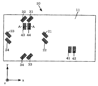
the present
invention and a cross section taken along line B-B in Fig. 20A;
Fig. 21A is a plan view illustrating a three-axis magnetic sensor of a third
15 embodiment in the present invention;
Fig. 21B is a sectional view illustrating the three-axis magnetic sensor of
the
third embodiment in the present invention and a cross section taken along line
A-A in
Fig. 21A;
Fig. 22A is a plan view schematically illustrating the pinning direction and
the
20 sensitivity direction of the three-axis magnetic sensor of the third
embodiment given in
Fig. 21A and an entire flat surface;
Fig. 22B is a perspective view schematically illustrating the pinning
direction
and the sensitivity direction of the three-axis magnetic sensor of the third
embodiment
given in Fig. 21 A and the enlarged A part in Fig. 22A;
25 Fig. 23A is a block diagram illustrating a bridge connection of the X-axis
sensor
CA 02601130 2007-09-13
26
of the third embodiment;
Fig. 23B is a block diagram illustrating a bridge connection of the Y-axis
sensor
of the third embodiment;
Fig. 23C is a block diagram illustrating a bridge connection of the Z-axis
sensor
of the third embodiment;
Fig. 24A is a plan view schematically illustrating a state of the heat
treatment for
regularization (pinning treatment) of the third embodiment;
Fig. 24B is a sectional view schematically illustrating a state of the heat
treatment for regularization (pinning treatment) in the third embodiment and a
cross
section taken along line A-A in Fig. 24A;
Fig. 25 is a plan view illustrating a three-axis magnetic sensor of a fourth
embodiment in the present invention;
Fig. 26A is a plan view schematically illustrating a three-axis magnetic
sensor of
a fifth embodiment in the present invention;
Fig. 26B is a sectional view schematically illustrating the three-axis
magnetic
sensor of the fifth embodiment in the present invention and a cross section
taken along
line A-A in Fig. 26A;
Fig. 27A is a view schematically illustrating a brief constitution of the
giant
magnetoresistive effect element used in the three-axis magnetic sensor of the
fifth
embodiment in the present invention and a plan view illustrating that a
plurality of giant
magnetoresistive effect element(GMR) bars are connected to form one giant
magnetoresistive effect element;
Fig. 27B is a view schematically illustrating a brief constitution of the
giant
magnetoresistive effect element used in the three-axis magnetic sensor of the
fifth
embodiment in the present invention and a sectional view schematically
illustrating a
CA 02601130 2007-09-13
27
cross section taken along line B-B' in Fig. 27A;
Fig. 27C is a view schematically illustrating a brief constitution of the
giant
magnetoresistive effect element used in the three-axis magnetic sensor of the
fifth
embodiment in the present invention and a view schematically illustrating an
inner
lamination state in Fig. 27B;
Fig. 28A is a view schematically illustrating the pinning direction and the
sensitivity direction of the three-axis magnetic sensor given in Fig. 26A and
a plan view
schematically illustrating an entire flat surface;
Fig. 28B is a view schematically illustrating the pinning direction and the
sensitivity direction of the three-axis magnetic sensor given in Fig. 26A and
a perspective
view schematically illustrating an enlarged C part in Fig. 28A;
Fig. 28C is a view schematically illustrating the pinning direction and the
sensitivity direction of the three-axis magnetic sensor given in Fig. 26A and
a perspective
view schematically illustrating an enlarged D part in Fig. 28A;
Fig. 29A is a block diagram illustrating a bridge connection of the X-axis
sensor
in the three-axis magnetic sensor of the fifth embodiment;
Fig. 29B is a block diagram illustrating a bridge connection of the Y-axis
sensor
in the three-axis magnetic sensor of the fifth embodiment;
Fig. 29C is a block diagram illustrating a bridge connection of the Z-axis
sensor
in the three-axis magnetic sensor of the fifth embodiment;
Fig. 30A is a view illustrating the heat treatment for regularization (pinning
treatment) in the three-axis magnetic sensor of the fifth embodiment and a
perspective
view schematically illustrating a bar magnet array used in the heat treatment
for
regularization (pinning treatment);
Fig. 30B is a view illustrating the heat treatment for regularization (pinning
CA 02601130 2007-09-13
28
treatment) in the three-axis magnetic sensor of the fifth embodiment and a
plan view
schematically illustrating a state of the heat treatment for regularization
(pinning
treatment);
Fig. 31A is a plan view illustrating a three-axis magnetic sensor of a sixth
embodiment in the present invention;
Fig. 31B is a sectional view illustrating the three-axis magnetic sensor of
the
sixth embodiment in the present invention and a cross section taken along line
E-E' in
Fig. 31 A;
Fig. 32A is a view schematically illustrating the pinning direction and the
sensitivity direction of the three-axis magnetic sensor of the sixth
embodiment in Fig.
31 A and a plan view schematically illustrating an entire flat surface;
Fig. 32B is a view schematically illustrating the pinning direction and the
sensitivity direction of the three-axis magnetic sensor of the sixth
embodiment in Fig.
31A and a perspective view schematically illustrating an enlarged F part in
Fig. 32A;
Fig. 32C is a view schematically illustrating the pinning direction and the
sensitivity direction of the three-axis magnetic sensor of the sixth
embodiment in Fig.
31 A and a perspective view schematically illustrating an enlarged G part in
Fig. 32A;
Fig. 33A is a block diagram illustrating a bridge connection of the X-axis
sensor
in the three-axis magnetic sensor of the sixth embodiment;
Fig. 33B is a block diagram illustrating a bridge connection of the Y-axis
sensor
in the three-axis magnetic sensor of the sixth embodiment;
Fig. 33C is a block diagram illustrating a bridge connection of the Z-axis
sensor
in the three-axis magnetic sensor of the sixth embodiment;
Fig. 34A is a view illustrating the heat treatment for regularization (pinning
treatment) in the three-axis magnetic sensor of the sixth embodiment and a
perspective
CA 02601130 2007-09-13
29
view schematically illustrating a bar magnet array used in the heat treatment
for
regularization (pinning treatment);
Fig. 34B is a view illustrating the heat treatment for regularization (pinning
treatment) in the three-axis magnetic sensor of the sixth embodiment and a
plan view
schematically illustrating a state of the heat treatment for regularization
(pinning
treatment);
Fig. 35A is a plan view illustrating the three-axis magnetic sensor of a
seventh
embodiment in the present invention;
Fig. 35B is a sectional view schematically illustrating the three-axis
magnetic
sensor of the seventh embodiment in the present invention and a cross section
taken
along line A-A' in Fig. 35A;
Fig. 36A is a view schematically illustrating a brief constitution of the
giant
magnetoresistive effect element used in the three-axis magnetic sensor of the
seventh
embodiment in the present invention and a plan view illustrating that a
plurality of giant
magnetoresistive effect element (GMR) bars are connected to form giant
magnetoresistive effect elements for one X-axis sensor;
Fig. 36B is a view schematically illustrating a brief constitution of the
giant
magnetoresistive effect element used in the three-axis magnetic sensor of the
seventh
embodiment in the present invention and a sectional view illustrating a cross
section
taken along line A-B' in Fig. 36A;
Fig. 36C is a view schematically illustrating a brief constitution of the
giant
magnetoresistive effect element used in the three-axis magnetic sensor of a
seventh
embodiment in the present invention and a view schematically illustrating an
inner
lamination state in Fig. 36B;
Fig. 37A is a plan view illustrating a state in which a plurality of giant
CA 02601130 2007-09-13
magnetoresistive effect element (GMR) bars of the seventh embodiment in the
present
invention are connected to form giant magnetoresistive effect elements for one
Y1-axis
sensor and giant magnetoresistive effect elements for one Y2-axis sensor;
Fig. 37B is a perspective view schematically illustrating a state of the C
part in
5 Fig. 37Awhen viewed obliquely from above;
Fig. 38A is a view schematically illustrating the pinning direction and the
sensitivity direction of the three-axis magnetic sensor given in Fig. 35A and
a plan view
schematically illustrating an entire flat surface;
Fig. 38B is a view schematically illustrating the pinning direction and the
10 sensitivity direction of the three-axis magnetic sensor given in Fig. 35A
and a perspective
view schematically illustrating an enlarged D part in Fig. 38A;
Fig. 38C is a view schematically illustrating the pinning direction and the
sensitivity direction of the three-axis magnetic sensor given in Fig. 35A and
a perspective
view schematically illustrating an enlarged E part in Fig. 38A;
15 Fig. 39A is a block diagram illustrating a bridge connection of the X-axis
sensor
in the seventh embodiment;
Fig. 39B is a block diagram illustrating a bridge connection of the Y1-axis
sensor in the seventh embodiment;
Fig. 39C is a block diagram illustrating a bridge connection of the Y2-axis
20 sensor in the seventh embodiment;
Fig. 40 is a plan view schematically illustrating a state of the heat
treatment for
regularization (pinning treatment) in the seventh embodiment;
Fig. 41 is a view explaining the heat treatment for regularization (pinning
treatment) in the seventh embodiment;
25 Fig. 42 is a plan view illustrating a brief constitution of the three-axis
magnetic
CA 02601130 2007-09-13
31
sensor in a first exemplified variation of the seventh embodiment of the
present
invention;
Fig. 43 is a plan view illustrating a brief constitution of the three-axis
magnetic
sensor in a second exemplified variation of the seventh embodiment of the
present
invention;
Fig. 44 is a plan view illustrating a brief constitution of the three-axis
magnetic
sensor in a third exemplified variation of the seventh embodiment of the
present
invention;
Fig. 45 is a plan view illustrating a brief constitution of the three-axis
magnetic
sensor in a fourth exemplified variation of the seventh embodiment of the
present
invention;
Fig. 46 is a plan view illustrating a brief constitution of the three-axis
magnetic
sensor in an eighth embodiment of the present invention;
Fig. 47A is a view illustrating an enlarged A part and an enlarged B part of
the
eight embodiment in Fig. 46 and a sectional view illustrating an enlarged
cross section
taken along line H-H' of the F part;
Fig. 47B is a view illustrating an enlarged Apart and an enlarged B part of
the
eight embodiment in Fig. 46 and a plan view illustrating an enlarged F part;
Fig. 47C is a view illustrating an enlarged A part and an enlarged B part of
the
eight embodiment in Fig. 46 and a sectional view illustrating an enlarged
cross section
taken along line H-H' of the G part;
Fig. 47D is a view illustrating an enlarged Apart and an enlarged B part of
the
eight embodiment in Fig. 46 and a plan view illustrating an enlarged G part;
Fig. 48 is a plan view illustrating a three-axis magnetic sensor of a ninth
embodiment in the present invention;
CA 02601130 2007-09-13
32
Fig. 49 is a plan view illustrating an X-axis GMR element used in the ninth
embodiment of the present invention;
Fig. 50 is a plan view illustrating a Z-axis GMR element used in the ninth
embodiment of the present invention;
Fig. 51 is a sectional view taken along line A-A in Fig. 50;
Fig. 52 is a block diagram illustrating a connection of the X-axis magnetic
sensor in the ninth embodiment of the present invention;
Fig. 53 is a block diagram illustrating a connection of the Y-axis magnetic
sensor
in the ninth embodiment of the present invention;
Fig. 54 is a block diagram illustrating a connection of the Z-axis magnetic
sensor in the ninth embodiment of the present invention;
Fig. 55 is a plan view illustrating an array arrangement on heat treatment for
regulation in the ninth embodiment of the present invention;
Fig. 56 is a sectional view taken along line B-B' in Fig. 55;
Fig. 57 is a plan view illustrating an array arrangement on polarization of
the
Z-axis GMR element of the ninth embodiment in the present invention;
Fig. 58 is a plan view illustrating a yoke used in a polarization process of
the
X-axis GMR element and the Y-axis GMR element of the ninth embodiment in the
present invention;
Fig. 59 is a schematic view illustrating a state of a magnetic field in the
yoke of
the ninth embodiment in the present invention;
Fig. 60 is a plan view illustrating a polarization process of the X-axis GMR
element and the Y-axis GMR element of the ninth embodiment in the present
invention;
Fig. 61 is a plan view illustrating a yoke used in the polarization process in
a
tenth embodiment of the present invention;
CA 02601130 2007-09-13
33
Fig. 62 is a schematic view illustrating a state of a magnetic field in a yoke
of
the tenth embodiment in the present invention;
Fig. 63A is a plan view schematically illustrating a conventional magnetic
sensor;
Fig. 63B is a side view schematically illustrating the conventional magnetic
sensor;
Fig. 64A is a view illustrating a bridge-connection of the conventional
magnetic
sensor;
Fig. 64B is a view illustrating a bridge-connection of the conventional
magnetic
sensor; and
Fig. 64C is a view illustrating a bridge-connection of the conventional
magnetic
sensor.
BEST MODE FOR CARRYING OUT THE INVENTION
[0041]
Hereinafter, an explanation will be made of features of the present invention
as a
three-axis magnetic sensor of a first embodiment to a tenth embodiment by
referring to
the drawings. However, the present invention is not restricted by these
embodiments
and appropriate modifications can be carried out, within a scope not departing
from the
spirit of the present invention.
[0042]
(First embodiment)
First, an explanation will be made of a three-axis magnetic sensor of a first
embodiment as follows by referring to Fig. lAto Fig. 15C.
[0043]
CA 02601130 2007-09-13
34
As illustrated in Fig. 1A and IB, a three-axis magnetic sensor 10 of the first
embodiment is provided with a substrate 11 made up of quartz or silicon, which
is in a
rectangular shape, with the sides along the X-axis and Y-axis orthogonal to
each other,
when viewed from above, (here, it is shaped so that the ratio of the short
side
(longitudinal) to the long side (transverse) (aspect ratio) is 1: 2 and the
side along the
X-axis is a long side and the side along the Y-axis is a short side) and has a
small
thickness in the direction of the Z-axis orthogonal to the X-axis and the Y-
axis. Then, a
total of 12 GMR elements respectively made up of four elements of X-axis GMR
elements 21 to 24, Y-axis GMR elements 31 to 34 and Z-axis GMR elements 41 to
44, a
total of 12 pads (not illustrated) and connecting wires (not illustrated)
connecting each of
the pads with each of the elements are fabricated on the substrate 11. An LSI
and a
wiring layer are also fabricated into the substrate 11. A substrate into which
the LSI is
fabricated is used to provide a magnetic sensor based on a digital output,
while a
substrate into which only the wiring layer is fabricated is used to provide a
magnetic
sensor based on an analog output.
[0044]
Here, the X-axis GMR elements are constituted with a first X-axis GMR
element 21, a second X-axis GMR element 22, a third X-axis GMR element 23 and
a
fourth X-axis GMR element 24. Then, the first X-axis GMR element 21 is
arranged at
approximately the center (hereinafter, referred to as the X-axis central
portion) between
the left end portion of the substrate 11 in the direction of the X-axis (here,
on the basis of
the left end portion in Fig. 1 A as a reference point of the X-axis, a right
direction of the
drawing from the reference point is regarded as a positive direction of the X-
axis, the
opposite direction is regarded as a negative direction of the X-axis, and the
same shall
apply hereinafter) and the right end portion, or above at approximately the
center
CA 02601130 2007-09-13
(hereinafter, referred to as the Y-axis central portion) between the lower end
portion in
the direction of the Y-axis (here, on the basis of the lower end portion in
Fig. 1 A as a
reference point of the Y-axis, an upper direction of the drawing from the
reference point
is regarded as a positive direction of the Y-axis, and the opposite direction
is regarded as
5 a negative direction of the Y-axis, and the same shall apply hereinafter)
and the upper end
portion, and the second X-axis GMR element 22 is arranged below thereof.
Further, the
third X-axis GMR element 23 is arranged above the Y-axis central portion in
the vicinity
of the X-axis left end portion on the substrate 11, and the fourth X-axis GMR
element 24
is arranged below thereof.
10 [0045]
Further, the Y-axis GMR elements are constituted with a first Y-axis GMR
element 31, a second Y-axis GMR element 32, a third Y-axis GMR element 33 and
a
fourth Y-axis GMR element 34. Then, the first Y-axis GMR element 31 is
arranged on
the right of approximately an intermediate portion from the X-axis central
portion to the
15 X-axis left end portion in the vicinity of the upper end portion of the
substrate I 1 in the
Y-axis direction, and the second Y-axis GMR element 32 is arranged left
thereof. The
third Y-axis GMR element 33 is arranged on the right of approximately an
intermediate
portion from the X-axis central portion to the X-axis left end portion in the
vicinity of the
lower end portion of the substrate 11 in the Y-axis direction, and the fourth
Y-axis GMR
20 element 34 is arranged left thereof.
[0046]
In addition, the Z-axis GMR elements are constituted with a first Z-axis GMR
element 41, a second Z-axis GMR element 42, a third Z-axis GMR element 43 and
a
fourth Z-axis GMR element 44. Then, the first Z-axis GMR element 41 is
arranged at
25 approximately an intermediate portion from the Y-axis central portion of
the substrate 11
CA 02601130 2007-09-13
36
to the Y-axis lower end portion or left at approximately an intermediate
portion from the
X-axis central portion to the X-axis right end portion, and the second Z-axis
GMR
element 42 is arranged right thereof. The third Z-axis GMR element 43 is
arranged at
approximately an intermediate portion from the Y-axis central portion of the
substrate 11
to the Y-axis upper end portion or left at approximately an intermediate
portion from the
X-axis central portion to the X-axis left end portion, and the fourth Z-axis
GMR element
44 is arranged right thereof.
[0047]
Here, each of the GMR elements 21 to 24, 31 to 34 and 41 to 44 is respectively
provided with four GMR bars mutually parallel and arranged adjacently in a
band form,
these four GMR bars are connected in series by using magnet films (bias magnet
films),
and magnet films which will act as a terminal are connected to these ends. For
example,
in Fig. 2A to 2B (it is to be noted that only the first X-axis GMR element 21
is illustrated
in Fig. 2A to 2C but other GMR elements are also similar in constitution),
four GMR
bars 21 a, 21 b, 21 c and 21 d are connected in series by the magnet films 21
f, 21 g, and 21 h,
and the magnet films 21 e and 21 i which will act as a terminal are connected
to these
ends.
[0048]
Here, each of the GMR bars (21a, 21b, 21c, 21d, etc.) of the X-axis GMR
elements 21 to 24 is formed on a flat surface parallel to the surface of a
substrate 11 and
arranged in such a way that the longitudinal direction gives an angle of 45
degrees with
respect to the X-axis. Further, each of the GMR bars of the Y-axis GMR
elements 31 to
34 is formed on a flat surface parallel to the surface of the substrate 11 and
arranged in
such a way that the longitudinal direction is orthogonal to the longitudinal
direction of
each of the GMR bars of the X-axis GMR elements 21 to 24. Further, each of the
GMR
CA 02601130 2007-09-13
37
bars of the Z-axis GMR elements 41 to 44 is arranged in such a way that one
GMR bar
(for example, 43a, 43b, 43c, 43d, or 44a, 44b, 44c, 44d, and the like (refer
to Fig. 1B))
per tilted surface (so as to give a tilted angle of approximately 45 degrees)
is formed on
each tilted surface of a plurality of projections (ledge portions) 15 formed
on the
substrate 11 and the cross section of which is in a trapezoidal shape, with
the longitudinal
direction being vertical to the X-axis and parallel to the Y-axis.
[0049]
Next, an explanation will be made of the constitution of the GMR bars by
exemplifying the GMR bar 21b of the first X-axis GMR element 21 on the basis
of Fig.
2Ato Fig. 2C. Other GMR bars 21a, 21c and 21d are also similar in constitution
and,
therefore, only the GMR bar 21b will be explained here. Further, an
explanation will
also be omitted of other X-axis GMR elements 22,23 and 24, the Y-axis GMR
elements
31, 32, 33 and 34 and the Z-axis GMR elements 41, 42, 43 and 44, which are
similar in
constitution.
[0050]
Here, as illustrated in Fig 2B, which is a schematic sectional view cut by a
flat
surface along line A-A in Fig. 2A, the GMR bar 21b of the first X-axis GMR
element 21
which is made of a spin valve film SV is a hard ferromagnetic body such as
CoCrPt
formed below both ends, and provided with magnet films (bias magnet film: hard
ferromagnetic body thin film layer) 21g and 21f made with a material having a
high
coercive force.
As the film constitution illustrated in Fig. 2C, the spin valve film SV is
constituted with a free layer (free layer and free magnetization layer) F, a
conductive
spacer layer S made with Cu having the thickness of 2.4nm (24A), a pin layer
(bonded
layer and fixed magnetization layer) P and a capping layer C made with
titanium (Ti) or
CA 02601130 2007-09-13
38
tantalum (Ta) having the thickness of 2.5nm (25A), which are laminated
sequentially on
the substrate 11.
[0051]
The free layer F is a layer in which the magnetization direction will change
according to the direction of an external magnetic field, and constituted with
a CoZrNb
amorphous magnetic layer 21b-1 formed immediately on the substrate 11 having
the
thickness of 8nm (80A), a NiFe magnetic layer 21b-2 formed on the CoZrNb
amorphous
magnetic layer 21b-1 having the thickness of 3.3nm (33A) and a CoFe layer 21b-
3
formed on the NiFe magnetic layer 21b-2 having the thickness of 1 to 3nm (10
to 30A).
The CoZrNb amorphous magnetic layer 21b-1 and the NiFe magnetic layer 21b-2
constitute a soft ferromagnetic thin film layer. The CoFe layer 21b-3 is
provided for
preventing the dispersion of Ni in the NiFe layer 21b-2 and Cu 21 b-4 in the
spacer layer
S.
[0052]
The pin layer P is prepared by adhering a CoFe magnetic layer 21b-5 having the
thickness of 2.2nm (22A) to an antiferromagnet film 21 b-6 made with a PtMn
alloy (Pt
content of 45 to 55mo1%) having the thickness of 24nm (240A). The CoFe
magnetic
layer 21b-5 constitutes a pinned layer in which the magnetization direction
(magnetization vector) is pinned (bonded) in the X-axis direction (here, a
negative
direction of the X-axis) by being backed in a manner of switched connection to
the
antiferromagnet film 21b-6 which is magnetized (magnetized).
[0053]
Further, bias magnet films 21e, 21f, 21g, 21h and 21i of the above-described
first X-axis GMR element 21 impart a bias magnetic field in a direction
parallel to the
longitudinal direction of each of the GMR bars with respect to a free layer F
(in the
CA 02601130 2007-09-13
39
direction tilted at -45 degrees with respect to the X-axis) in order to
maintain an uniaxial
anisotropy of the free layer F. Then, the CoFe magnetic layer 21b-5 (the same
will
apply to other GMR bars 21 a, 21 c and 21 d) is backed in a manner of switched
connection to the antiferromagnet film 21b-6, thereby constituting a pinned
layer in such
a way that the magnetization direction (magnetization vector) is pinned
(bonded) in a
positive direction of the X-axis (in the direction given by the solid-line
arrow al in Fig.
3A). Similarly, the second X-axis GMR element 22 imparts a bias magnetic field
in a
direction parallel to the longitudinal direction of each of the GMR bars (in
the direction
tilted at -45 degrees with respect to the X-axis). Then, the pinned layer is
formed in
such a way that the magnetization direction (magnetization vector) is pinned
(bonded) in
a positive direction of the X-axis (in the direction given by the solid-line
arrow b1 in Fig.
3A).
[0054]
Thereby, in the first X-axis GMR element 21 and the second X-axis GMR
element 22, the sensitivity direction of a magnetic field is a direction
vertical to the
longitudinal direction of each of the GMR bars, namely, the direction tilted
at 45 degrees
with respect to a positive direction of the X-axis (in the direction given by
the
broken-line arrows a2 and b2 in Fig. 3A). Where a magnetic field is applied in
the
direction given by the broken-line arrows a2 and b2 in Fig. 3A, resistance
values of the
first X-axis GMR element 21 and the second X-axis GMR element 22 will decrease
proportionally with an increase in magnetic field. Where the magnetic field is
applied
in the direction opposite that given by the broken-line arrows a2 and b2 in
Fig. 3A,
resistance values of the first X-axis GMR element 21 and the second X-axis GMR
element 22 will increase proportionally with an increase in magnetic field.
[0055]
CA 02601130 2007-09-13
In contrast, in the third X-axis GMR element 23 and the fourth X-axis GMR
element 24, the bias magnet film imparts a bias magnetic field in a direction
opposite 180
degrees to the first X-axis GMR element 21 and the second X-axis GMR element
22 or
in a direction parallel to the longitudinal direction of each of the GMR bars
(in the
5 direction tilted at 45 degrees with respect to a negative direction of the X-
axis). Then, a
pinned layer is formed in such a way that the magnetization direction
(magnetization
vector) is pinned (bonded) in a negative direction of the X-axis (in the
direction given by
the solid-line arrows cl and dl in Fig. 3A or the direction opposite 180
degrees to the
magnetization direction of the pinned layer of the first X-axis GMR element 21
and the
10 second X-axis GMR element 22).
[0056]
Thereby, the sensitivity direction of a magnetic field is a direction vertical
to the
longitudinal direction of each of the GMR bars, namely, the direction given by
the
broken-line arrows c2 and d2 in Fig. 3A (the direction opposite 180 degrees to
the
15 sensitivity direction of the first X-axis GMR element 21 and the second X-
axis GMR
element 22). Where a magnetic field is applied in the direction given by the
broken-line
arrows c2 and d2 in Fig. 3A, resistance values of the third X-axis GMR element
23 and
the fourth X-axis GMR element 24 will decrease proportionally with an increase
in
magnetic field. Where the magnetic field is applied in the direction opposite
that given
20 by the broken-line arrows c2 and d2 in Fig. 3A, resistance values of the
third X-axis
GMR element 23 and the fourth X-axis GMR element 24 will increase
proportionally
with an increase in magnetic field.
[0057]
Further, in the first Y-axis GMR element 31 and the second Y-axis GMR element
25 32, a bias magnet film imparts a bias magnetic field in a direction
parallel to the
CA 02601130 2007-09-13
41
longitudinal direction of each of the GMR bars (in the direction tilted at 45
degrees with
respect to a positive direction of the X-axis, namely, the direction in which
the bias
magnetic field of the first X-axis GMR element 21 and the second X-axis GMR
element
22 is turned counterclockwise 90 degrees) and a pinned layer is formed in such
a way
that the magnetization direction (magnetization vector) is pinned (bonded) in
a positive
direction of the Y-axis (in the direction given by the solid-line arrows el
and fl in Fig.
3A).
[0058]
Thereby, the sensitivity direction of a magnetic field is a direction vertical
to the
longitudinal direction of each of the GMR bars, namely, the direction tilted
at 45 degrees
with respect to a negative direction of the X-axis (the direction given by the
broken-line
arrows e2 and f2 in Fig. 3A). Where a magnetic field is applied in the
direction given
by the broken-line arrows e2 and f2 in Fig. 3A, resistance values of the first
Y-axis GMR
element 31 and the second Y-axis GMR element 32 will decrease proportionally
with an
increase in magnetic field. Where the magnetic field is applied in the
direction opposite
that given by the broken-line arrows e2 and fl in Fig. 3A, resistance values
of the first
Y-axis GMR element 31 and the second Y-axis GMR element 32 will increase
proportionally with an increase in magnetic field.
[0059]
In contrast, in the third Y-axis GMR element 33 and the fourth Y-axis GMR
element 34, the bias magnet film imparts a bias magnetic field in a direction
opposite 180
degrees to the first Y-axis GMR element 31 and the second Y-axis GMR element
32 or in
a direction parallel to the longitudinal direction of each of the GMR bars (in
the direction
tilted at -45 degrees with respect to a negative direction of the X-axis).
Then, a pinned
layer is formed in such a way that the magnetization direction (magnetization
vector) is
CA 02601130 2007-09-13
42
pinned (bonded) in a negative direction of the Y-axis (in the direction given
by the
solid-line arrows gl and hl in Fig. 3A)
[0060]
Thereby, the sensitivity direction of a magnetic field is a direction vertical
to the
longitudinal direction of each of the GMR bars, namely, the direction tilted
at -45
degrees with respect to a positive direction of the X-axis (the direction
given by the
broken-line arrow g2 and h2 in Fig. 3A, and opposite 180 degrees to the
magnetization
direction of the first Y-axis GMR element 31 and the second Y-axis GMR element
32).
Where a magnetic field is applied in the direction given by the broken-line
arrows g2 and
h2 in Fig. 3A, resistance values of the third Y-axis GMR element 33 and the
fourth Y-axis
GMR element 34 will decrease proportionally with an increase in magnetic
field.
Where the magnetic field is applied in the direction opposite that given by
the
broken-line arrows g2 and h2 in Fig. 3A, resistance values of the third Y axis
GMR
element 33 and the fourth Y-axis GMR element 34 will increase proportionally
with an
increase in magnetic field.
[0061]
Further, in the first Z-axis GMR element 41 and the second Z-axis GMR
element 42, as illustrated schematically in Fig. 3B, bias magnet films 41f,
41g and 41h
(42f, 42g and 42h) impart a bias magnetic field in a direction parallel to the
longitudinal
direction of each of the GMR bars 41a, 41b, 41c and 41d (42a, 42b, 42c and
42d),
namely, on a flat surface of each tilted surface (the tilted angle is
approximately 45
degrees) of projections (ledge portions) 15, a direction in which the
longitudinal direction
is vertical to the X-axis and parallel to the Y-axis. Then, a pinned layer is
formed in
such a way that the magnetization direction (magnetization vector) is pinned
(bonded) in
the direction tilted at 45 degrees with respect to a positive direction of the
Z-axis (in the
CA 02601130 2007-09-13
43
direction given by the solid-line arrows i 1(j 1) in Fig. 3B).
[0062]
Then, each of these GMR bars 41 a, 41b, 41 c and 41 d (42a, 42b, 42c and 42d)
is
connected in series by bias magnet films 41f, 41g and 41h (42t 42g and 42h).
Thereby,
the sensitivity direction of a magnetic field is a direction vertical to the
longitudinal
direction of each of the GMR bars, namely, the direction given by the broken-
line arrows
i2 (j2) in Fig. 3B having a positive component of the Z-axis (the direction
moving from
the back to the front on the page space). Where a magnetic field is applied in
the
direction given by the broken-line arrows i2 (j2) in Fig. 3B, resistance
values of the first
Z-axis GMR element 41 and the second Z-axis GMR element 42 will decrease
proportionally with an increase in magnetic field. Where the magnetic field is
applied
in the direction opposite that given by the broken-line arrows i2 02) in Fig.
3B,
resistance values of the first Z-axis GMR element 41 and the second Z-axis GMR
element 42 will increase proportionally with an increase in magnetic field.
[0063]
In contrast, in the third Z-axis GMR element 43 and the fourth Z-axis GMR
element 44, as illustrated schematically in Fig. 3C, the bias magnet films
43f, 43g and
43h (44~ 44g and 44h) impart a bias magnetic field in a direction parallel to
the
longitudinal direction of each of the GMR bars 43a, 43b, 43c and 43d (44a,
44b, 44c and
44d), namely, on a flat surface of each tilted surface (the tilted angle is
approximately 45
degrees) of projections (ledge portions) 15, a direction in which the
longitudinal direction
is vertical to the X-axis and parallel to the Y-axis. Then, a pinned layer is
formed in
such a way that the magnetization direction (magnetization vector) is pinned
(bonded) in
the direction tilted at 45 degrees with respect to a negative direction of the
Z-axis (in the
direction given by the solid-line arrows kl (11) in Fig. 3C.
CA 02601130 2007-09-13
44
[0064]
Then, each of these GMR bars, 43a, 43b, 43c and 43d (44a, 44b, 44c and 44d) is
connected in series by the bias magnet films 43f, 43g and 44h (44f, 44g and
44h).
Thereby, the sensitivity direction of a magnetic field is a direction vertical
to the
longitudinal direction of each of the GMR bars, namely, the direction given by
the
broken-line arrows k2 (12) in Fig. 3C having a positive component of the Z-
axis (the
direction moving from the back to the front on the page space). Where a
magnetic field
is applied in the direction given by the broken-line arrows k2 (12) in Fig.
3C, resistance
values of the third Z-axis GMR element 43 and the fourth Z-axis GMR element 44
will
decrease proportionally with an increase in magnetic field. Where the magnetic
field is
applied in the direction opposite that given by the broken-line arrows k2 (12)
in Fig. 3C,
resistance values of the third Z-axis GMR element 43 and the fourth Z-axis GMR
element 44 will increase proportionally with an increase in magnetic field.
[0065]
As an equivalent circuit illustrated in Fig. 4A, the X-axis magnetic sensor is
constituted with the first X-axis GMR element 21 to the fourth X-axis GMR
element 24,
which are full-bridge- connected. In Fig. 4A, the arrows indicate the
magnetization
direction of a bonded layer on which each of the GMR elements 21 to 24 is
pinned. In
the above constitution, a pad 25 and a pad 26 are connected to a positive
electrode and a
negative electrode of a constant voltage source 29, thereby imparting a
potential Vxin+
(3V in this embodiment) and a potential Vxin- (0(V) in this embodiment). Then,
potentials of a pad 27 and a pad 28 are output respectively as a potential
Vxout+ and a
potential Vxout-, and a potential difference between them (Vxout+ - Vxout-) is
output as
a sensor output Vxout.
[0066]
CA 02601130 2007-09-13
As an equivalent circuit illustrated in Fig. 4B, the Y-axis magnetic sensor is
constituted with the first Y-axis GMR element 31 to the fourth Y-axis GMR
element 34,
which are full-bridge- connected. Apad 35 and a pad 36 are connected to a
positive
electrode and a negative electrode of a constant voltage source 39, thereby
imparting a
5 potential Vyin+ (3V in this embodiment) and a potential Vyin- (0(V) in this
embodiment),
and a potential difference between a pad 37 and a pad 38 is output as a sensor
output
Vyout.
[0067]
As an equivalent circuit illustrated in Fig. 4C, the Z-axis magnetic sensor is
10 constituted with the first Z-axis GMR element 41 to the fourth Z-axis GMR
element 44,
which are full-bridge- connected. Then, a pad 45 and a pad 46 are connected to
a
positive electrode and a negative electrode of a constant voltage source 49,
thereby
imparting a potential Vzin+ (3V in this embodiment) and a potential Vzin-
(0(V) in this
embodiment), and a potential difference between a pad 47 and a pad 48 is
output as a
15 sensor output Vzout.
[0068]
Next, an explanation will be made of a method for manufacturing the
above-constituted three-axis magnetic sensor by referring to schematic
sectional views,
namely, Fig. 5A, Fig. 5B, Fig. 5C through Fig. 14A, Fig. 14B and Fig. 14C.
Fig. 5A,
20 Fig. 6A, Fig. 7A, to Fig. 14A illustrate via portions, Fig. 5B, Fig. 6B,
Fig. 7B to Fig. 14B
illustrate pad portions, Fig. SC, Fig. 6C, Fig. 7C to Fig. 14C illustrate GMR
portions of
Z-axis. Here, as described above, it is preferable to use a substrate in which
an LSI is
fabricated in advance by a CMOS process or one in which only a wiring layer is
fabricated in advance as the substrate 11.
25 [0069]
CA 02601130 2007-09-13
46
In the method for manufacturing the three-axis magnetic sensor, as illustrated
in
Fig. 5Ato Fig. 5C, first, an interlayer insulation film I lb made up of, for
example,
silicon oxide film or silicon nitride film is coated on a substrate (quartz
substrate or
silicon substrate) I 1 having a wiring layer I la by using the SOG (spin on
glass) method
or CMP method, thereby giving a smooth surface. Thereafter, as illustrated in
Fig. 6A
to Fig. 6C, the interlayer insulation film I lb at the via portion and the pad
portion is
removed by etching to create openings l lc and l ld. Then, as illustrated in
Fig. 7Ato
Fig. 7C, a Si02 film (thickness: 1500A)lle and a Si3N4 film (thickness:
5000A)l lf are
formed on the surface of each of the openings by plasma CVD.
[0070]
Next, as illustrated in Fig. 8A to Fig. 8C, a resist is coated thereon and cut
in
such a pattern to create openings at a via portion and a pad portion.
Thereafter, the
Si3N4 film I If at the via portion and the pad portion is removed by etching
to remove the
resist. Thereby, openings 11 g and 11 h are formed at the via portion and the
pad portion,
but the Si02 film 11 e is treated so as not to be completely etched but to
remain thereon.
Here, in order to prevent water from permeating into a wiring layer or an LSI
due to
exposure of an interlayer insulation film l lb at openings I lc and lld, the
openings 11g
and 11 h are made smaller in dimension than the openings l l c and l i d.
[0071]
Thereafter, as illustrated in Fig. 9Ato 9C, a Si02 film (thickness: 5p.m)l li
is
formed thereon by using plasma CVD. Next, a resist is coated thereon to form a
resist
film (thickness: 5 m)l lj. The thus formed resist film (thickness: 5 m) I lj
is cut in
such a pattern to create openings at the via portion and the pad portion and
also cut in
such a pattern to provide projections (ledge portions) 15 for arranging Z-axis
GMR
elements 41, 42, 43 and 44. After cutting, the resist film l lj is subjected
to heat
CA 02601130 2007-09-13
47
treatment at 150 C for 10 minutes, and the cut portion of the resist film 11 j
is formed in a
tapered shape (tapering) as illustrated in Fig. l0A to IOC.
[0072]
Thereafter, dry etching is conducted under the conditions where the SiO2 film
(thickness: 5pm) lli and the resist film (thickness: 5 m) l lj are etched
approximately at
a similar ratio and the Si02 film 11 i after the etching remains to be about
5000A at the
greatest thickness portion. Here, openings of the SiO2 film 11 i at the via
portion and the
pad should not be greater in dimension than openings on the Si3N4 film 11f at
the via
portion and the pad portion. After the dry etching, any remaining resist is
removed.
Thereby, as illustrated in Fig. 11Ato 11C, projections (ledge portions) 15
made of the
Si02 film 11 i are formed at GMR portions.
[0073]
Next, a resist is coated thereon, the coated resist is cut in such a pattern
as to
create openings at the via portion, and etching is conducted. Thereafter, any
remaining
resist is removed to create an opening l lk at the via portion, as illustrated
in Fig. 12A to
12C, thereby exposing a wiring layer 11 a, and the uppermost layer of the
substrate 11.
Then, sputtering is conducted to form a primary film made with Ti or Cr
(thickness:
300 m).
[0074]
Next, a bias magnet film 11m having a high coercive force, which is a hard
ferromagnetic body made with a material such as CoCrPt, (later converted to 21
e, 21 f,
21g, 21h, 21i, etc., as illustrated in Fig. 2A) is formed on the surface of
the primary film
by sputtering, vacuum evaporation or ion plating. A resist is coated thereon,
the thus
coated resist is cut in a pattern of the bias magnet film, and then, the bias
magnet film
11 m and the primary film are etched. Prior to the etching, it is preferable
that the resist
CA 02601130 2007-09-13
48
be reflowed by heat treatment to remove corners of the resist (rounding) for
the purpose
of conducting an appropriate etching on a tilted surface of each of the
projections (ledge
portions) 15. Thereafter, any remaining resist is removed. Then, sputtering is
conducted to form a GMR multilayer film 11 n that will act as GMR elements
(later,
converted to 21 to 24, 31 to 34, 41 to 44, etc.) on the surface.
[0075]
As illustrated in Fig. 2C, the GMR multilayer film l i n is constituted with a
free
layer (free layer, free magnetization layer) F, a conductive spacer layer S
made with Cu
having the thickness of 2.4nm (24A), a pin layer (bonded layer, fixed
magnetization
layer) P and a capping layer C made with titanium (Ti) or tantalum (Ta) having
the
thickness of 2.5nm (25A), which are laminated sequentially on the substrate
11. Then,
the film layer F is constituted with a CoZrNb amorphous magnetic layer 21b-1
formed
immediately on the substrate 11 having the thickness of 8nm (80A), a NiFe
magnetic
layer 21b-2 having the thickness of 3.3nm (33A) and a CoFe layer 21b-3 having
the
thickness of 1 to 3nm (10 to 30A). The CoZrNb amorphous magnetic layer 21b-1
and
the NiFe magnetic layer 21b-2 constitute a soft ferromagnetic thin film layer.
The pin
layer P is prepared by adhering the CoFe magnetic layer 21b-5 having the
thickness of
2.2nm (22A) to the antiferromagnet film 21b-6 having the thickness of 24nm
(240A).
[0076]
Next, a permanent magnet array is allowed to move close to the thus obtained
laminated body to conduct heat treatment for regularization (pinning
treatment), thereby
fixing the magnetization direction of the pinned layer P. Here, as
schematically illustrated
in Fig. 15A to 15C, the heat treatment for regularization (pinning treatment)
is conducted
by arranging a permanent bar magnet array (magnet array) arranged in a lattice
form so
as to be mutually different in polarity of the upper end (lower end) of
adjacent permanent
CA 02601130 2007-09-13
49
bar magnet pieces in such a way that the N pole is arranged above the center
of a region
left from the center of a substrate 11 and the S pole is arranged above the
center of a
region right from the center of the substrate 11.
[0077]
As is apparent from Fig. 15Ato 15C (it is to be noted that Fig. 15Ato 15C
illustrate a state that only six-permanent magnet pieces are arranged), on the
lower
surface of a permanent bar magnet piece arranged above the center of a region
left from
the center of a substrate 11, a magnetic field is formed, which is different
in direction at
every 90 degrees moving from one N pole toward S poles adjacent to the N pole
at the
shortest distance. In contrast, on the lower surface of the permanent bar
magnet piece
arranged above the center of a region right from the center of the substrate
11, a magnetic
field is formed, which is different at every 90 degrees moving to one S pole
from N poles
adjacent to the S pole at the shortest distance. These magnetic fields are
utilized to
conduct heat treatment for fixing the magnetization direction of the bonded
layer P
(pinned layer of the bonded layer P). More specifically, in a state given in
Fig. 15A to
15C, the substrate 11 and the permanent bar magnet array (magnet array) are
fixed,
heated in vacuum at temperatures from 260 C to 290 C, and allowed to stand
approximately for four hours as they are, thereby conducting the heat
treatment for
regularization (pinning treatment).
[0078]
Thereby, as illustrated in Fig. 3A to 3C, in the first X-axis GMR element 21
and
the second X-axis GMR element 22, the magnetization direction of a pinned
layer is
fixed to the direction given by the arrows al and bl in Fig. 3A, while in the
third X-axis
GMR element 23 and the fourth X-axis GMR element 24, the magnetization
direction of
the pinned layer is fixed in the direction given by the arrows cl and dl in
Fig. 3A.
CA 02601130 2007-09-13
Further, in the first Y-axis GMR element 31 and the second Y-axis GMR element
32, the
magnetization direction of the pinned layer is fixed to the direction given by
the arrows
el and fl in Fig. 3A, while in the third Y-axis GMR element 33 and the fourth
Y-axis
GMR element 34, the magnetization direction of the pinned layer is fixed to
the direction
5 given by the arrows gi and hl in Fig. 3A. In the first Z-axis GMR element 41
and the
second Z-axis GMR element 42, the magnetization direction of the pinned layer
is fixed
to a direction tilted at 45 degrees from the X-axis to a positive direction of
the Z-axis
inside a tilted surface of each of the projections (ledge portions) 15. In the
third Z-axis
GMR element 43 and the fourth Z-axis GMR element 44, the magnetization
direction of
10 the pinned layer is fixed to a direction tilted at 45 degrees from the X-
axis to a negative
direction of the Z-axis inside the tilted surface of each of the projections
(ledge portions)
15.
[0079]
Thereafter, a resist is coated on the surface of a GMR multilayer film 11 n so
as
15 to give a predetermined thickness, for example, 2 m, at a flat portion, a
mask is arranged
on the surface of the resist, printing and development are conducted to remove
an
unnecessary resist, thereby forming a resist film having the same pattern as
the GMR
multilayer film l ln to be obtained later. Here, in order to give an
appropriate etching to
projections (ledge portions) 15, it is preferable that prior to the etching,
the resist be
20 reflowed by heat treatment to remove corners of the resist (rounding).
Thereafter, a
portion of the GMR multilayer film 1 ln not covered with the resist film is
removed by
ion milling to form a GMR multilayer film l ln in a predetermined shape (for
example, a
plurality of narrow bands). Here, a via portion is treated so that both the
GMR
multilayer film l ln and a bias magnet film l lm are allowed to remain. This
is to
25 prevent possible breakage of wiring due to the edge of the via portion.
CA 02601130 2007-09-13
51
[0080]
Next, the resist film is removed. As illustrated in Fig. 14A to Fig. 14C, a
Si3N4
film 11 o is formed on the above films at the thickness of 10000A. by using
plasma CVD,
and a polyimide film l lp is then formed thereon to provide a protective film.
Thereafter, the polyimide film llp on a pad portion is used as a mask, the
Si3N4 film 11o
at the pad portion is removed by etching to provide an opening to the pad
portion,
thereby forming individual pads. A wiring is provided for connecting these
pads and
the substrate 11 is finally cut. According to the processes described so far,
the
three-axis magnetic sensor 10 of the first embodiment illustrated in Fig. 1 A
and 1B is
fabricated.
[0081]
(Exemplified variation of the first embodiment)
In the above-described three-axis magnetic sensor of the first embodiment, an
arrangement relationship of each of the GMR elements can be changed in various
ways,
thereby providing exemplified variations. Hereinafter, an explanation will be
made
simply of a representative exemplified variation of the three-axis magnetic
sensor in the
first embodiment by referring to Fig. 16A to 16D. Whether to select the
arrangement
relationship of each of the GMR elements in the first embodiment or that of
each of the
GMR elements in the following exemplified variation may be appropriately
decided,
depending on an LSI circuit and the like formed on the substrate.
[0082]
(First exemplified variation)
Fig. 16A is a brief constitution view schematically illustrating a three-axis
magnetic sensor 50a of a first exemplified variation. In the first exemplified
variation,
Z-axis GMR elements are changed in arrangement relationship. More
specifically, as
CA 02601130 2007-09-13
52
illustrated in Fig. 16A, a first Z-axis GMR element 51i is arranged at
approximately an
intermediate portion from the Y-axis central portion of the substrate 51 to
the Y-axis
upper end portion or left at approximately an intermediate portion from the X-
axis
central portion to the X-axis right end portion, and a second Z-axis GMR
element 51j is
arranged right thereof. Further, a third Z-axis GMR element 51k is arranged at
approximately an intermediate portion from the Y-axis central portion of the
substrate 51
to the Y-axis lower end portion or left at approximately an intermediate
portion from the
X-axis central portion to the X-axis left end portion, and a fourth Z-axis GMR
element
511 is arranged right thereof. Here, the X-axis GMR elements S la to 51d and
the Y-axis
GMR elements 51e to 51h are the same as the X-axis GMR elements 21 to 24 and
the
Y-axis GMR elements 31 to 34 in the above-described first embodiment.
[0083J
(Second exemplified variation)
Fig. 16B is a brief constitution view schematically illustrating a three-axis
magnetic sensor 50b of a second exemplified variation. In the second
exemplified
variation, Y-axis GMR elements are changed in arrangement relationship. More
specifically, as illustrated in Fig. 16B, a first Y-axis GMR element 52e is
arranged on the
right of approximately an intermediate portion from the X-axis central portion
to the
X-axis right end portion in the vicinity of the Y-axis upper end portion of
the substrate 52,
and a second Y-axis GMR element 52f is arranged left thereof. Further, a third
Y-axis
GMR element 52g is arranged on the right of approximately an intermediate
portion from
the X-axis central portion to the X-axis right end portion in the vicinity of
the Y-axis
lower end portion of the substrate 52, and a fourth Y-axis GMR element 52h is
arranged
left thereof. Here, the X-axis GMR elements 52a to 52d and the Z-axis GMR
elements
52i to 521 are the same as the X-axis GMR elements 21 to 24 and the Z-axis GMR
CA 02601130 2007-09-13
53
elements 41 to 44 in the above-described first embodiment.
[0084]
(Third exemplified variation)
Fig. 16C is a brief constitution view schematically illustrating a three-axis
magnetic sensor 50c of a third exemplified variation. In the third exemplified
variation,
X-axis GMR elements are changed in arrangement relationship. More
specifically, as
illustrated in Fig. 16C, a first X-axis GMR element 53a is arranged above the
Y-axis
central portion in the vicinity of the X-axis right end portion of the
substrate 53, and a
second X-axis GMR element 53b is arranged below thereof. Further, a third X-
axis
GMR element 53c is arranged at the X-axis central portion of the substrate 53
or above
the Y-axis central portion, and a fourth X-axis GMR element 53d is arranged
below
thereof. Here, the Y-axis GMR elements 53e to 53h and the Z-axis GMR elements
53i
to 531 are the same as the Y-axis GMR elements 31 to 34 and the Z-axis GMR
elements
41 to 44 in the above-described first embodiment.
[0085]
(Fourth exemplified variation)
Fig. 16D is a brief constitution view schematically illustrating a three-axis
magnetic sensor 50d of a fourth exemplified variation. In the fourth
exemplified
variation, Y-axis GMR elements and Z-axis GMR elements are changed in
arrangement
relationship. More specifically, as illustrated in Fig. 16D, a first Y-axis
GMR element
54e is arranged on the right of approximately an intermediate portion from the
X-axis
central portion to the X-axis left end portion in the vicinity of the Y-axis
upper end
portion of the substrate 54, and a second Y-axis GMR element 54f is arranged
left thereof.
Further, a third Y-axis GMR element 54g is arranged on the right of
approximately an
intermediate portion from the X-axis central portion to the X-axis right end
portion in the
CA 02601130 2007-09-13
54
vicinity of the Y-axis upper end portion of the substrate 54, and a fourth Y-
axis GMR
element 54h is arranged left thereof. Still finther, a first Z-axis GMR
element 54i is
arranged at approximately an intermediate portion from the Y-axis central
portion of the
substrate 54 to the Y-axis upper end portion or left at approximately an
intermediate
pordon from the X-axis central portion to the X-axis right end portion, and
the second
Z-axis GMR element 54j is arranged right thereof. A third Z-axis GMR element
54k is
arranged at approximately an intermediate portion from the Y-axis central
portion of the
substrate 54 to the Y-axis lower end portion or left at approximately an
intermediate
portion from the X-axis central portion to the X-axis left end portion, and a
fourth Z-axis
GMR element 541 is arranged right thereof. Here, the X-axis GMR elements 54a
to 54d
are the same as the X-axis GMR elements 21 to 24 in the above-described first
embodiment.
[0086]
(Second embodiment)
Next, an explanation will be made of a three-axis magnetic sensor of a second
embodiment as follows by referring to Fig. 17A to Fig. 20C.
[0087]
As illustrated in Fig. 17A and 17B, a three-axis magnetic sensor 60 of the
second embodiment is provided with a substrate 61 made with quartz or silicon
which is
in a rectangular shape with the sides along the X-axis and Y-axis orthogonal
to each other,
when viewed from above (here, it is shaped so that the ratio of the short side
(longitudinal), to the long side (transverse) (aspect ratio) is 1: 1.5 and the
side along the
X-axis is a long side and the side along the Y-axis is a short side) and has a
small
thickness in the direction of the Z-axis orthogonal to the X-axis and the Y-
axis. It is
possible to make the present sensor smaller in dimension than the three-axis
magnetic
CA 02601130 2007-09-13
sensor of the first embodiment by using the above-described substrate 61.
[0088]
Then, a total of 12 GMR elements made up of respectively four elements of
X-axis GMR elements 61 a to 61 d, Y-axis GMR elements 61 e to 61 h and Z-axis
GMR
5 elements 61i to 611, a total of 12 pads (not illustrated) and connecting
wires (not
illustrated) connecting each of the pads with each of the elements are
fabricated into the
substrate 61. An LSI and a wiring layer are also fabricated on the substrate
61 as with
the substrate 11 of the first embodiment. A substrate into which the LSI is
fabricated is
used to provide a magnetic sensor based on a digital output, while a substrate
into which
10 only the wiring layer is fabricated is used to provide a magnetic sensor
based on an
analog output.
[0089]
Here, the X-axis GMR elements are constituted with a first X-axis GMR
element 61 a, a second X-axis GMR element 61b, a third X-axis GMR element 61c
and a
15 fourth X-axis GMR element 61d. Then, the first X-axis GMR element 61a is
arranged
at approximately a 2/3 portion from the X-axis left end portion of the
substrate 61 to the
right end portion or above the Y-axis central portion, and the second X-axis
GMR
element 61b is arranged below thereof. Further, the third X-axis GMR element
61 c is
arranged above the Y-axis central portion in the vicinity of the X-axis left
end portion of
20 the substrate 61, and the fourth X-axis GMR element 61d is arranged below
thereof.
[0090]
Further, the Y-axis GMR elements are constituted with a first Y-axis GMR
element 61e, a second Y-axis GMR element 61f, a third Y-axis GMR element 61g
and a
fourth Y-axis GMR element 61h. Then, the first Y-axis GMR element 61e is
arranged
25 on the right at approximately a 1/3 portion from the X-axis left end
portion to the right
CA 02601130 2007-09-13
56
end portion in the vicinity of the Y-axis upper end portion of the substrate
61, and the
second Y-axis GMR element 61f is arranged left thereof. Further, the third Y-
axis GMR
element 61g is arranged on the right of approximately a 1/3 portion from the X-
axis left
end portion to the right end portion in the vicinity of the Y-axis lower end
portion of the
substrate 61, and the fourth Y-axis GMR element 61h is arranged left thereof.
[0091]
In addition, the Z-axis GMR elements are constituted with a first Z-axis GMR
element 61 i, a second Z-axis GMR element 61 j, a third Z-axis GMR element 61
k and a
fourth Z-axis GMR element 611. Then, the first Z-axis GMR element 61 i is
arranged at
an intermediate portion between approximately a 2/3 portion from the X-axis
left end
portion of the substrate 61 to the right end portion and the right end portion
or above the
Y-axis central portion, and the second Z-axis GMR element 61 j is arranged
below thereof.
Further, the third Z-axis GMR element 61k is arranged at an intermediate
portion
between approximately a 1/3 portion from the X-axis left end portion of the
substrate 61
to the right end portion and a 2/3 portion or above the Y-axis central
portion, and the
fourth Z-axis GMR element 611 is arranged below thereof.
[0092]
Each of the GMR elements 61a to 61d, 61 e to 61h and 61i to 611 is provided
with four GMR bars mutuaUy parallel and arranged adjacently in a band form,
these four
GMR bars are connected in series by magnet films (bias magnet films), and
magnet films
which will act as a terminal are connected to these ends.
Here, each of the GMR bars of the X-axis GMR elements 61 a to 61 d is formed
on a flat surface parallel to the surface of a substrate 61 and arranged in
such a way that
the longitudinal direction gives an angle of 45 degrees with respect to the X-
axis.
Further, each of the GMR bars of the Y-axis GMR elements 61e to 61h is formed
on a
CA 02601130 2007-09-13
57
flat surface parallel to the surface of the substrate 61 and arranged in such
a way that the
longitudinal direction is orthogonal to each of the GMR bars of the X-axis GMR
elements 61 a to 61 d.
[0093]
Further, as illustrated in Fig. 17B, Fig. 18B and 18C, each of the GMR bars of
the Z-axis GMR elements 61i to 611 is arranged in such a way that one GMR bar
(61i-1,
61i-2, 61i-3 or 61i-4 (61j-1, 61j-2, 61j-3 and 61j4) or 61k-1, 61k-2, 61k-3
and 61k-4
(611-1, 611-2, 611-3 and 611-4)) per tilted surface (so as to give a tilted
angle of
approximately 45 degrees) is formed on each tilted surface of a plurality of
projections
(ledge portions) 65 formed on the substrate 61 and the cross section of which
is in a
trapezoidal shape, with the longitudinal direction being parallel to the X-
axis and vertical
to the Y-axis.
[0094]
The three-axis magnetic sensor 60 of the second embodiment is different from
the three-axis magnetic sensor 10 of the first embodiment in that the
substrate 61 is 2/3 in
dimension as compared with the substrate 11 of the first embodiment and the Z-
axis
GMR elements 61i to 611 are different in arrangement position, but similar in
other
constitutions to the three-axis magnetic sensor 10 of the first embodiment.
[0095]
Here, in the X-axis GMR elements 61a and 61b, a bias magnet film imparts a
bias magnetic field in a direction parallel to the longitudinal direction of
each of the
GMR bars (the direction tilted at -45 degrees with respect to a position
direction of the
X-axis). Then, a pinned layer is formed in such a way that the magnetization
direction
(magnetization vector) is pinned (bonded) in a positive direction of the X-
axis (in the
direction given by the solid-line arrows al and b 1 in Fig. 18A). Further, in
the third
CA 02601130 2007-09-13
58
X-axis GMR element 61c and the fourth X-axis GMR element 61d, the bias magnet
film
imparts a bias magnetic field in a direction parallel to the longitudinal
direction of each
of the GMR bars (in the direction tilted at 45 degrees with respect to a
negative direction
of the X-axis). The pinned layer is formed in such a way that the
magnetization
direction (magnetization vector) is pinned (bonded) in a negative direction of
the X-axis
(in the direction given by the solid-line arrows cl and dl in Fig. 18A and
opposite 180
degrees to the magnetization direction of the first X-axis GMR element 61a and
the
second X-axis GMR element 61b).
[0096]
Therefore, in the first X-axis GMR element 61 a and the second X-axis GMR
element 61b, the sensitivity direction of a magnetic field is a direction
vertical to the
longitudinal direction of each of the GMR bars, namely, the direction tilted
at 45 degrees
with respect to a positive direction of the X-axis (the direction given by the
broken-line
arrows a2 and b2 in Fig. 18A). In contrast, in the third X-axis GMR element
61c and
the fourth X-axis GMR element 61d, the sensitivity direction of a magnetic
field is a
direction vertical to the longitudinal direction of each of the GMR bars,
namely, the
direction tilted at 45 degrees with respect to a negative direction of the X-
axis (the
direction given by the broken-line arrows c2 and d2 in Fig. 18A and opposite
180 degrees
to the sensitivity direction of the first X-axis GMR element 61a and the
second X-axis
GMR element 61b.
[0097]
Further, in the first Y-axis GMR element 61e and the second Y-axis G1VIR
element 61f, a bias magnet film imparts a bias magnetic field in a direction
parallel to the
longitudinal direction of each of the GMR bars (the direction tilted at 45
degrees with
respect to a positive direction of the X-axis, namely, the direction in which
the bias
CA 02601130 2007-09-13
59
magnetic field of the X-axis GMR elements 61 a and 61b is turned
counterclockwise 90
degrees). Then, a pinned layer is formed in such a way that the magnetization
direction
(magnetization vector) is pinned (bonded) in a positive direction of the Y-
axis (the
direction given by the solid-line arrows e1 and fl in Fig. 18A). In contrast,
in the third
Y-axis GMR element 61g and the fourth Y-axis GMR element 61h, the bias magnet
film
imparts a bias magnetic field in the direction opposite 180 degrees to the
first Y-axis
GMR element 61e and the second Y-axis GMR element 61f and parallel to the
longitudinal direction of each of the GMR bars (the direction tilted at -45
degrees with
respect to a negative direction of the X-axis). Then, the pinned layer is
formed in such
a way that the magnetization direction (magnetization vector) is pinned
(bonded) in a
negative direction of the Y-axis (the direction given by the solid-line arrows
gl and hl in
Fig. 18A).
[0098]
Therefore, in the first Y-axis GMR element 61 e and the second Y-axis GMR
element 61f, the sensitivity direction of a magnetic field is a direction
vertical to the
longitudinal direction of each of the GMR bars, namely, the direction tilted
at -45 degrees
with respect to a negative direction of the X-axis (the direction given by the
broken-line
arrows e2 and f2 in Fig. 18A). In contrast, in the third Y-axis GMR element
61g and the
fourth Y-axis GMR element 61h, the sensitivity direction is a direction
vertical to the
longitudinal direction of each of the GMR bars, namely, the direction tilted
at -45 degrees
with respect to a positive direction of the X-axis (the direction given by the
broken-line
arrows g2 and h2 in Fig. 18A and opposite 180 degrees to the magnetization
direction of
the first Y-axis GMR element 61 e and the second Y-axis GMR element 61 fl.
[0099]
Further, in the first Z-axis GMR element 61i and the second Z-axis GMR
CA 02601130 2007-09-13
element 61j, as schematically illustrated in Fig. 18B, the bias magnet films
61 i-5, 61 i-6
and 61i-7 (61j-5, 61j-6 and 61j-7) impart a bias magnetic field in a direction
parallel to
the longitudinal direction of each of the GMR bars 61i-1, 61 i-2, 61 i-3 and
61 i-4 (61 j-1,
61j-2, 61j-3 and 61j-4), namely, on a flat surface of each tilted surface (the
tilted angle is
5 approximately 45 degrees) of projections (ledge portions) 65, a direction in
which the
longitudinal direction is parallel to the X-axis and vertical to the Y-axis.
Then, a pinned
layer is formed in such a way that the magnetization direction (magnetization
vector) is
pinned (bonded) in the direction tilted at 45 degrees from a positive
direction of the
X-axis to a positive direction of the Z-axis inside each tilted surface of the
projections
10 (ledge portions) 65 (the direction given by the solid-line arrows i 1(j 1)
in Fig. 18B).
[0100]
Then, these GMR bars, 61i-1, 61i-2, 61i-3 and 61i-4 (61j-1, 61j-2, 61j-3 and
61 j-4) are connected in series with the bias magnet films 61 i-5, 61 i-6 and
61 i-7 (61 j-5,
61 j-6 and 61 j-7). Thereby, the sensitivity direction of a magnetic field is
a direction
15 vertical to the longitudinal direction of each of the GMR bars, namely, the
direction
given by the broken-line arrows i2 (j2) in Fig. 18B having a positive
component of the
Z-axis (the direction moving from the back to the front on the page space).
Where a
magnetic field is applied in the direction given by the broken-line arrows i2
(j2) in Fig.
18B, resistance values of the first Z-axis GMR element 61i and the second Z-
axis GMR
20 element 61 j will decrease proportionally with an increase in magnetic
field. Where the
magnetic field is applied in the direction opposite that given by the broken-
line arrows i2
02) in Fig. 18B, resistance values of the first Z-axis GMR element 61i and the
second
Z-axis GMR element 61j will increase proportionally with an increase in
magnetic field.
[0101]
25 In contrast, in the third Z-axis GMR element 61k and the fourth Z-axis GMR
CA 02601130 2007-09-13
, . = .
61
element 611, as schematically illustrated in Fig. 18C, the bias magnet films
61k-5, 61k-6
and 61k-7 (611-5, 611-6 and 611-7) impart a bias magnetic field in a direction
parallel to
the longitudinal direction of each of the GMR bars 61k-1, 61k-2, 61k-3 and 61k-
4 (611-1,
6112, 611-3 and 611-4), namely, on a flat surface of each tilted surface (the
tilted angle is
approximately 45 degrees) of projections (ledge portions) 65, or a direction
in which the
longitudinal direction is parallel to the X-axis and vertical to the Y-axis.
Then, a pinned
layer is formed in such a way that the magnetization direction (magnetization
vector) is
pinned (bonded) in the direction tilted at 45 degrees from a positive
direction of the
X-axis to a negative direction of the Z-axis inside each tilted surface of the
projections
(ledge portions) 65 (the direction given by the solid-line arrows kl (11) in
Fig. 18C).
[0102]
Then, these GMR bars, 61k-1, 61k-2, 61k-3 and 61k-4 (611-1, 611-2, 611-3 and
611-4) are connected in series with the bias magnet films 61k-5, 61k-6 and 61k-
7 (611-5,
611-6 and 611-7). Thereby, the sensitivity direction of a magnetic field is a
direction
vertical to the longitudinal direction of each of the GMR bars, namely, the
direction
given by the broken-line arrows i2 (j2) in Fig. 18B having a negative
component of the
Z-axis (the direction moving from the back to the front on the page space).
Where a
magnetic field is applied in the direction given by the broken-line arrows k2
(12) in Fig.
18C, resistance values of the third Z-axis GMR element 61k and the fourth Z-
axis GMR
element 611 will decrease proportionally with an increase in magnetic field.
Where the
magnetic field is applied in the direction opposite that given by the broken-
line arrows k2
(12) in Fig. 18C, resistance values of the third Z-axis GMR element 61k and
the fourth
Z-axis GMR element 611 will increase proportionally with an increase in
magnetic field.
[0103]
As an equivalent circuit illustrated in Fig. 19A, the X-axis magnetic sensor
is
CA 02601130 2007-09-13
62
constituted with the first X-axis GMR element 61a to the fourth X-axis GMR
element
61d, which are full-bridge-connected. In Fig. 19A, the arrows indicate the
magnetization direction of a bonded layer on which each of the GMR elements
61a to
64d is pinned. In the above constitution, a pad 62a and a pad 62b are
connected to a
positive electrode and a negative electrode of a constant voltage source 62e,
thereby
imparting a potential Vxin+ (3V in this embodiment) and a potential Vxin-
(0(V) in this
embodiment). Then, potentials of a pad 62c and a pad 62d are output
respectively as a
potential Vxout+ and a potential Vxout-, and a potential difference between
them
(Vxout+ - Vxout-) is output as a sensor output Vxout.
[0104]
As an equivalent circuit illustrated in Fig. 19B, the Y-axis magnetic sensor
is
constituted with the first Y-axis GMR element 61e to the fourth Y-axis GMR
element 61h,
which are full-bridge-connected. Then, a pad 63a and a pad 63b are connected
to a
positive electrode and a negative electrode of a constant voltage source 63e,
thereby
imparting a potential Vyin+ (3V in this embodiment) and a potential Vyin-
(0(V) in this
embodiment), and a potential difference between a pad 63c and a pad 63d is
output as a
sensor output Vyout.
[0105]
As an equivalent circuit illustrated in Fig. 19c, the Z-axis magnetic sensor
is
constituted with the first Z-axis GMR element 61i to the fourth Z-axis GMR
element 611,
which are full-bridge-connected. Then, a pad 64a and a pad 64b are connected
to a
positive electrode and a negative electrode of a constant voltage source 64e,
thereby
imparting a potential Vyin+ (3V in this embodiment) and a potential Vyin-
(0(V) in this
embodiment), and a potential difference between a pad 64c and a pad 64d is
output as a
sensor output Vyout.
CA 02601130 2007-09-13
63
[0106]
Since the three-axis magnetic sensor 60 of the second embodiment is
manufactured by a method similar to that for the three-axis magnetic sensor 10
of the
first embodiment, an explanation for the method wi11 be omitted here. However,
a brief
explanation will be made as follows for heat treatment for regularization
(pinning
treatment).
[0107]
As schematically illustrated in Fig. 20 A to 20C, in the heat treatment for
regularization (pinning treatment) for manufacturing the three-axis magnetic
sensor 60 of
the second embodiment, a permanent bar magnet array (magnet array) is
prepared, which
is arranged in a lattice form so as to be mutually different in polarity from
the upper end
(lower end) of adjacent permanent bar magnet pieces.
Thereby, an N pole is arranged, with the center given to a point where a line
dividing the long side of a substrate 61 at a 1/3 portion intersects with a
line dividing the
short side of the substrate 61 at a 1/2 portion, and S poles are arranged at
positions
symmetrical to the four directions (above, below, right and left), with the
center given to
the N pole. The S poles above and below and either of the left S pole or the
right S pole
are arranged outside the substrate 61. The remaining S pole is arranged with
the center
placed on the short side of the substrate 61. Thereby, as illustrated in Fig.
18A to 18C, a
magnetic field in a positive direction of the X-axis is imparted to the first
X-axis GMR
element 61 a and the second X-axis GMR element 61b. A magnetic field in a
negative
direction of the X-axis is imparted to the third X-axis GMR element 61 c and
the fourth
X-axis GMR element 61d.
[0108]
Further, a magnetic field in a positive direction of the Y-axis is imparted to
the
CA 02601130 2007-09-13
64
first Y-axis GMR element 61e and the second Y-axis GMR element 61f, while a
magnetic
field in a negative direction of the Y-axis is imparted to the third Y-axis
GMR element
61g and the fourth Y-axis GMR element 61h. In addition, a magnetic field in
the
direction tilted at 45 degrees from a positive direction of the X-axis to a
positive
direction of the Z-axis inside a tilted surface of each of the projections
(ledge portions)
65 is imparted to the first Z-axis GMR element 61i and the second Z-axis GMR
element
61j. A magnetic field in the direction tilted at 45 degrees from a positive
direction of
the X-axis to a negative direction of the Z-axis inside the tilted surface of
each of the
projections (ledge portions) 65 is imparted to the fourth Z-axis GMR element
61k and the
fourth Z-axis GMR element 611.
Fig. 20A to 20C illustrate an example where the S pole is on the right short
side
of the substrate 61. In the present embodiment, in a substrate adjacent to the
right, the S
pole is arranged on the left short side of the substrate. When this substrate
is turned 180
degrees, the output symbols are reverse to those obtained in Fig. 20A to 20C.
Further, in all the embodiments to be described later, the polarity is
inevitably
reversed in some of the adjacent chips.
[0109]
(Third embodiment)
Then, an explanation will be made of the three-axis magnetic sensor of a third
embodiment as follows by referring to Fig. 21A to Fig. 24B.
[0110]
As illustrated in Fig. 21A and 21B, a three-axis magnetic sensor 70 of the
third
embodiment is provided with a substrate 71 made with quartz or silicon which
is in a
square shape having the sides along the X-axis and Y-axis orthogonal to each
other, when
viewed from above, (namely, half in dimension as compared with the substrate
11 of the
CA 02601130 2007-09-13
first embodiment) and has a small thickness in the direction of the Z-axis
orthogonal to
the X-axis and the Y-axis. It is possible to make the present sensor smaller
in dimension
than the three-axis magnetic sensor of the first embodiment and that of the
second
embodiment by using the above-described substrate 71.
5 [0111]
Then, a total of ten GMR elements, namely, four each of the X-axis GMR
elements 71a to 71d and the Y-axis GMR elements 71e to 71h and two Z-axis GMR
elements 71i to 71j formed on a substrate 71, two non-magnetic resistors 71k
to 711, a
total of 12 pads (not illustrated) formed on the substrate 71 and connect.ing
wires (not
10 illustrated) connecting each of the pads with each of the elements are
fabricated. An
LSI and a wiring layer are also fabricated into the substrate 71, as with the
substrate 11 of
the first embodiment. A substrate into which the LSI is fabricated is used to
provide a
magnetic sensor based on a digital output, while a substrate into which only
the wiring
layer is fabricated is used to provide a magnetic sensor based on an analog
output.
15 [0112]
Here, the X-axis GMR elements are constituted with a first X-axis GMR
element 71a, a second X-axis GMR element 71b, a third X-axis GMR element 71c
and a
fourth X-axis GMR element 71d. Then, the first X-axis GMR element 71a is
arranged
above the Y-axis central portion in the vicinity of the X-axis right end
portion, and the
20 second X-axis GMR element 71b is arranged below thereof. Further, the third
X-axis
GMR element 71c is arranged above the Y-axis central portion in the vicinity
of the
X-axis left end portion, and the fourth X-axis GMR element 71d is arranged
below
thereof.
[0113]
25 Further, the Y-axis GMR elements are constituted with a first Y-axis GMR
CA 02601130 2007-09-13
66
element 71e, a second Y-axis GMR element 71f, a third Y-axis GMR element 71 g
and a
fourth Y-axis GMR element 71h. Then, the first Y-axis GMR element 71 e is
arranged
on the right of the X-axis central portion in the vicinity of the Y axis upper
end portion,
and the second Y-axis GMR element 71f is arranged left thereof. Further, the
third
Y-axis GMR element 71g is arranged on the right of the X-axis central portion
in the
vicinity of the Y-axis lower end portion, and the fourth Y-axis GMR element 71
h is
arranged left thereof.
[0114]
In addition, the Z-axis GMR elements are constituted with a first Z-axis GMR
element 71 i and a second Z-axis GMR element 71j as well as a first non-
magnetic
resistor 71k and a second non-magnetic resistor 711 for bridge-connecting
them. Then,
the first Z-axis GMR element 71i is arranged at an intermediate portion from
the Y-axis
central portion to the Y-axis upper end portion or left at the X-axis central
portion, and
the second Z-axis GMR element 71j is arranged right thereof. Further, the
first
non-magnetic resistor 71k is arranged at an intermediate portion from the Y-
axis central
portion to the Y-axis lower end portion or left at the X-axis central portion,
and the
second non-magnetic resistor 711 is arranged right thereof.
[0115]
Each of the GMR elements 71a to 71d, 71e to 71h and 71i and 71j is provided
with four GMR bars mutually parallel and arranged adjacently in a band form,
these four
GMR bars are connected in series by magnet films (bias magnet films), and the
magnet
films which will act as a terminal are connected to these ends.
Here, each of the GMR bars of the X-axis GMR elements 71a to 71d is formed
on a flat surface parallel to the surface of a substrate 71 and arranged in
such a way that
the longitudinal direction gives an angle of 45 degrees with respect to the X-
axis.
CA 02601130 2007-09-13
67
Further, each of the GMR bars of the Y-axis GMR elements 71 e to 71h is formed
on a
flat surface parallel to the surface of the substrate 71 and arranged in such
a way that the
longitudinal direction intersects with each of the GMR bars of the X-axis GMR
elements
71a to 71d (here, to be orthogonal).
[0116]
Further, as illustrated in Fig. 21B and Fig. 22B, each of the GMR bars of the
Z-axis GMR elements 71 i and 71j is arranged in such a way that one GMR bar
(71 i-1,
71i-2, 71i-3 or 71i-4 (71j-1, 71j-2, 71j-3 or 71j-4)) per tilted surface (so
as to give a tilted
angle of approximately 45 degrees) is formed on each tilted surface of a
plurality of
projections (ledge portions) 75 formed on the substrate 71 and the cross
section of which
is in a trapezoidal shape, with the longitudinal direction being parallel to
the X-axis and
vertical to the Y-axis. Further, the non-magnetic resistors 71k to 711 are
formed on a
flat surface parallel to the surface of the substrate 71 and arranged in such
a way that the
longitudinal direction is vertical to the X-axis and parallel to the Y-axis.
[0117]
The three-axis magnetic sensor 70 of the third embodiment is different from
the
three-axis magnetic sensor 10 of the first embodiment in that the substrate 71
is square in
shape and half in dimension as compared with the substrate 11 of the first
embodiment
and provided with two Z-axis GMR elements 71i to 71j and two non-magnetic
resistors
71k to 711, but similar in other constitutions to the three-axis magnetic
sensor 10 of the
first embodiment.
[0118]
Here, in the X-axis OMR elements 71a and 71b, a bias magnet film imparts a
bias magnetic field in a direction parallel to the longitudinal direction of
each of the
GMR bars (the direction tilted at 45 degrees with respect to a positive
direction of the
CA 02601130 2007-09-13
68
X-axis). Then, a pinned layer is formed in such a way that the magnetization
direction
(magnetization vector) is pinned (bonded) in a positive direction of the X-
axis (in the
direction given by the solid-line arrows al and bl in Fig. 17A). Further, in
the third
X-axis GMR element 71c and the fourth X-axis GMR element 71d, the bias magnet
film
imparts a bias magnetic field in a direction parallel to the longitudinal
direction of each
of the GMR bars (in the direction tilted at 45 degrees with respect to a
negative direction
of the X-axis).
The pinned layer is formed in such a way that the magnetization direction
(magnetization vector) is pinned (bonded) in a negative direction of the X-
axis (in the
direction given by the solid-line arrows cl and dl in Fig. 17A and opposite
180 degrees
to the magnetization direction of the first X-axis GMR element 71a and the
second
X-axis GMR element 71b).
[0119]
Therefore, in the first X-axis GMR element 71 a and the second X-axis GMR
element 71b, the sensitivity direction of a magnetic field is a direction
vertical to the
longitudinal direction of each of the G1VIR bars, namely, the direction tilted
at -45 degrees
with respect to a positive direction of the X-axis (the direction given by the
broken-line
arrows a2 and b2 in Fig. 22A). In contrast, in the third X-axis GMR element
71c and
the fourth X-axis GMR element 71d, the sensitivity direction of a magnetic
field is a
direction vertical to the longitudinal direction of each of the GMR bars,
namely, a
direction tilted at -45 degrees with respect to a negative direction of the X-
axis (the
direction given by the broken-line arrows c2 and, d2 in Fig. 22A and opposite
180
degrees to the sensitivity direction of the first X-axis GMR element 71a and
the second
X-axis GMR element 71b).
[0120]
CA 02601130 2007-09-13
69
Further, in the first Y-axis GMR element 71e and the second Y-axis GMR
element 71C a bias magnet film imparts a bias magnetic field in a direction
parallel to the
longitudinal direction of each of the GMR bars (the direction tilted at -45
degrees with
respect to a position direction of the X-axis, namely, the direction in which
the bias
magnetic field of the X-axis GMR elements 71a and 71b is turned
counterclockwise 90
degrees). Then, a pinned layer is formed in such a way that the magnetization
direction
(magnetization vector) is pinned (bonded) in a positive direction of the Y-
axis (the
direction given by the solid-line arrows e I and fl in Fig. 22A). In contrast,
in the third
Y-axis GMR element 71g and the fourth Y-axis GMR element 71h, the bias magnet
film
imparts a bias magnetic field in the direction opposite 180 degrees to the
first Y-axis
GMR element 71e and the second Y-axis GMR element 71f and parallel to the
longitudinal direction of each of the GMR bars (the direction tilted at -45
degrees with
respect to a negative direction of the X-axis). Then, the pinned layer is
formed in such
a way that the magnetization direction (magnetization vector) is pinned
(bonded) in a
negative direction of the Y-axis (the direction given by the solid-line arrows
gl and hl in
Fig. 22A).
[0121]
Therefore, in the first Y-axis GMR element 71e and the second Y-axis GMR
element 71f, the sensitivity direction of a magnetic field is a direction
vertical to the
longitudinal direction of each of the GMR bars, namely, the direction tilted
at -45 degrees
with respect to a positive direction of the Y-axis (the direction given by the
broken-line
arrows e2 and fl in Fig. 22A). In contrast, in the third Y-axis GMR element
71g and the
fourth Y-axis GMR element 71h, the sensitivity direction is a direction
vertical to the
longitudinal direction of each of the GMR bars, namely, the direction tilted
at -45 degrees
with respect to a negative direction of the Y-axis (the direction given by the
broken-line
CA 02601130 2007-09-13
arrows g2 and h2 in Fig. 22A and opposite 180 degrees to the magnetization
direction of
the first Y-axis GMR element 71e and the second Y-axis GMR element 71f).
[0122]
Further, in the first Z-axis GMR element 71i and the second Z-axis GMR
5 element 71j, as schematically illustrated in Fig. 22B, the bias magnet films
71 i-5, 71i-6
and 71 i-7 (71 j-5, 71 j-6 and 71 j-7) impart a bias magnetic field in a
direction parallel to
the longitudinal direction of each of the GMR bars 71i-1, 71i-2, 71i-3 and 71i-
4 (71j-1,
71j-2, 71j-3 and 71j-4), namely, on a flat surface of each tilted surface (the
tilted angle is
approximately 45 degrees) of projections (ledge portions)75, a direction in
which the
10 longitudinal direction is vertical to the X-axis and parallel to the Y-
axis. Then, a pinned
layer is formed in such a way that the magnetization direction (magnetization
vector) is
pinned (bonded) in a direction tilted at 45 degrees from a positive direction
of the Y-axis
to a negative direction of the Z-axis inside each tilted surface of the
projections (ledge
portions) 75 (the direction given by the solid-line arrow il in Fig. 22B).
15 [0123]
Then, these GMR bars, 71i-1, 71i-2, 71i-3 and 71i-4 (71j-1, 71j-2, 71j-3 and
71 j-4) are connected in series with the bias magnet films 71 i-5, 71 i-6 and
71 i-7 (71 j-5,
71j-6 and 71j-7). Thereby, the sensitivity direction of a magnetic field is a
direction
vertical to the longitudinal direction of each of the GMR bars, a negative
direction of the
20 Z-axis, namely, the direction given by the broken-line arrow i2 in Fig. 22B
(the direction
moving from the back to the front on the page space). Where a magnetic field
is
applied in the direction given by the broken-line arrows i2 in Fig. 22B,
resistance values
of the first Z-axis GMR element 71i and the second Z-axis GMR element 71j will
decrease proportionally with an increase in magnetic field. Where the magnetic
field is
25 applied in the direction opposite that given by the broken-line arrows i2
in Fig. 22B,
CA 02601130 2007-09-13
71
resistance values of the first Z-axis GMR element 71i and the second Z-axis
GMR
element 71 j will increase proportionally with an increase in magnetic field.
[0124]
In contrast, the first non-magnetic resistor 71k and the second non-magnetic
resistor 71k are made with a non-magnetic body such as polysilicon. Further,
in the
third embodiment, the first non-magnetic resistor 71k is arranged at
approximately a 1/4
portion in a positive direction of the Y-axis or left at approximately the X-
axis central
portion, and the second non-magnetic resistor 711 is arranged right thereof.
However,
the first non-magnetic resistor 71k and the second non-magnetic resistor 711
may be
arranged at any place on the substrate 71.
[0125]
As an equivalent circuit illustrated in Fig. 23A, the X-axis magnetic sensor
is
constituted with the first X-axis GMR element 71a to the fourth X-axis GMR
element
71d, which are full-bridge-connected. In Fig. 23A, the arrows indicate the
magnetization direction of a bonded layer on which each of the GMR elements
71a to
74d is pinned. In the above constitution, a pad 72a and a pad 72b are
connected to a
positive electrode and a negative electrode of a constant voltage source 72e,
thereby
imparting a potential Vxin+ (3V in this embodiment) and a potential Vxin-
(0(V) in this
embodiment). Then, potentials of a pad 72c and a pad 72d are output
respectively as a
potential Vxout+ and a potential Vxout-, and a potential difference between
them
(Vxout+ - Vxout-) is output as a sensor output Vxout.
[0126]
As an equivalent circuit illustrated in Fig. 23B, the Y-axis magnetic sensor
is
constituted with the first Y-axis GMR element 71e to the fourth Y-axis GMR
element 71h,
which are full-bridge-connected. Then, a pad 73a and a pad 73b are connected
to a
CA 02601130 2007-09-13
72
positive electrode and a negative electrode of a constant voltage source 73e,
thereby
imparting a potential Vyin+ (3V in this embodiment) and a potential Vyin-
(0(V) in this
embodiment), and a potential difference between a pad 73c and a pad 73d is
output as a
sensor output Vyout.
[0127]
As an equivalent circuit illustrated in Fig. 23C, the Z-axis magnetic sensor
is
constituted with the first Z-axis GMR element 71i, the second Z-axis GMR
element 71j,
the first non-magnetic resistor 71k, and the second non-magnetic resistor 711,
which are
full-bridge-connected. Then, a pad 74a and a pad 74b are connected to a
positive
electrode and a negative electrode of a constant voltage source 74e, thereby
imparting a
potential Vyin+ (3V in this embodiment) and a potential Vyin- (0(V) in this
embodiment).
Further, a potential difference between a pad 74c and a pad 74d is output as a
sensor
output Vyout.
[0128]
Since the three-axis magnetic sensor 70 of the third embodiment is
manufactured by a method similar to that for the three-axis magnetic sensor 10
of the
first embodiment excluding fabrication of the first non-magnetic resistor 71k
and the
second non-magnetic resistor 711, an explanation for the method will be
omitted here.
However, a brief explanation will be made as follows for heat treatment for
regularization (pinning treatment).
[0129]
As schematically illustrated in Fig. 24 A and Fig. 24B, in the heat treatment
for
regularization (pinning treatment) for manufacturing the three-axis magnetic
sensor 70 of
the third embodiment, a permanent bar magnet array (magnet array) is prepared,
which is
arranged in a lattice fonm so as to be mutually different in polarity of the
upper end
CA 02601130 2007-09-13
73
(lower end) of adjacent permanent bar magnet pieces. Thereby, an N pole is
arranged
above the center of the substrate 71, and S poles are arranged above outside a
substrate
71 at positions symmetrical to four directions (above, below, right and left),
with the
center given to the N pole.
Thereby, as illustrated in Fig. 22A and Fig. 22B, a magnetic field in a
positive
direction of the X-axis is imparted to the first X-axis GMR element 71a and
the second
X-axis GMR element 71b. A magnetic field in a negative direction of the X-axis
is
imparted to the third X-axis GMR element 71c and the fourth X-axis GMR element
71d.
Further, a magnetic field in a positive direction of the Y-axis is imparted to
the first
Y-axis GMR element 71e and the second Y-axis GMR element 71f, and a magnetic
field
in a negative direction of the Y-axis is imparted to the third Y-axis GMR
element 71g and
the fourth Y-axis GMR element 71h. In addition, a magnetic field in the
direction tilted
at 45 degrees from a positive direction of the Y-axis to a negative direction
of the Z-axis
inside a tilted surface of each of the projections (ledge portions) 75 (the
direction moving
from the back to the front in Fig. 22A and Fig. 22B) is imparted to the first
Z-axis GMR
element 71 i and the second Z-axis GMR element 71 j.
[0130]
(Fourth embodiment)
Next, an explanation will be made for the three-axis magnetic sensor of a
fourth
embodiment as follows by referring to Fig. 25.
As illustrated in Fig. 25, a three-axis magnetic sensor 80 of the fourth
embodiment is provided with a substrate 81 made with quartz or silicon which
is in a
rectangular shape with the sides along the X-axis and Y-axis orthogonal to
each other,
when viewed from above (here, it is shaped so that the ratio of the short side
(longitudinal) to the long side (transverse) (aspect ratio) is 1: 2 and the
side along the
CA 02601130 2007-09-13
74
X-axis is a long side and the side along the Y-axis is a short side) and has a
small
thickness in the direction of the Z-axis orthogonal to the X-axis and the Y-
axis.
[0131]
Then, a total of 12 GMR elements made up of respectively four elements of
X-axis GMR elements 81a to 81d, Y-axis GMR elements 81e to 81h and Z-axis GMR
elements 81 i to 811, a total of 12 pads (not illustrated) and connecting
wires (not
illustrated) connecting each of the pads with each of the elements are
fabricated on a
substrate 81. An LSI and a wiring layer are also fabricated into the substrate
81, as with
the substrate 11 of the first embodiment. A substrate into which the LSI is
fabricated is
used to provide a magnetic sensor based on a digital output, while a substrate
into which
only the wiring layer is fabricated is used to provide a magnetic sensor based
on an
analog output.
[0132]
Here, the X-axis GIv1R elements are constituted with a first X-axis GMR
element 81a, a second X-axis GMR element 81b, a third X-axis GMR element 81c
and a
fourth X-axis GMR element 81d. The longitudinal direction of each of the GMR
elements is arranged in a direction parallel to the Y-axis. Then, the first X-
axis GMR
element 81a is arranged at the X-axis central portion or above the Y-axis
central portion,
and the second X-axis GMR element 81b is arranged below thereof. Further, the
third
X-axis GMR element 81 c is arranged above the Y-axis central portion in the
vicinity of
the X-axis left end portion, and the fourth X-axis GMR element 81d is arranged
below
thereof.
[0133]
Further, the Y-axis GMR elements are constituted with a first Y-axis GMR
element 81e, a second Y-axis GMR element 81f, a third Y-axis GMR element 9 1g
and a
CA 02601130 2007-09-13
fourth Y-axis GMR element 81h. The longitudinal direction of each of the GMR
elements is arranged in a direction parallel to the X-axis. Then, the first Y-
axis GMR
element 81 e is arranged on the right of an intermediate portion from the X-
axis central
portion to the X-axis left end portion in the vicinity of the Y-axis upper end
portion, and
5 the second Y-axis GMR element 81f is arranged left thereof. Further, the
third Y-axis
GMR element 81g is arranged on the right of an intermediate portion from the X-
axis
central portion to the X-axis left end portion in the vicinity of the Y-axis
lower end
portion, and the fourth Y-axis G1vlIR element 81h is arranged left thereof.
[0134]
10 In addition, the Z-axis GMR elements are constituted with a first Z-axis
GMR
element 81i, a second Z-axis GMR element 81j, a third Z-axis GMR element 81k
and a
fourth Z-axis GMR element 811. The longitudinal direction of each of the GMR
elements
is given in a direction parallel to the Y-axis. Then, the first Z-axis GMR
element 81i is
arranged at an intermediate portion from the Y-axis central portion to the Y-
axis lower
15 end portion or right at an intermediate portion from the X-axis central
portion to the
X-axis right end portion, and the second Z-axis GMR element 81j is arranged
left thereof.
Further, the third Z-axis GMR element 81k is arranged at an intermediate
portion from
the Y-axis central portion to the Y-axis upper end portion or right at an
intermediate
portion from the X-axis central portion to the X-axis left end portion, and
the fourth
20 Z-axis GMR element 811 is arranged left thereof.
The above-arranged constitution is also able to provide a three-axis magnetic
sensor similar in constitution to the three-axis magnetic sensors described in
the first, the
second and the third embodiments.
[0135]
25 (Fifth embodiment)
CA 02601130 2007-09-13
76
Next, an explanation will be made for the three-axis magnetic sensor of a
fifth
embodiment as follows by referring to Fig. 26Ato Fig. 30B.
[0136}
As illustrated in Fig. 26A and Fig. 26B, a three-axis magnetic sensor 110 of
the
fifth embodiment is provided with a substrate 11 made with quartz or silicon
which is in
a rectangular shape with the sides along the X-axis and Y-axis orthogonal to
each other,
when viewed from above (here, it is shaped so that the ratio of the short side
(longitudinal) to the long side (transverse) (aspect ratio) is 1: 2 and the
side along the
X-axis is a long side and the side along the Y-axis is a short side) and has a
small
thickness in the direction of the Z-axis orthogonal to the X-axis and the Y-
axis. Then, a
total of 12 GMR elements made up of respectively four elements of X-axis GMR
elements 112a to 112d, Y-axis GMR elements 112e to 112h and Z-axis GMR
elements
112i to 1121, a pad portion (a portion which takes out an output from a
wiring, not
illustrated), a via portion (a portion connected to the wiring from GMR
elements, but the
via portion is not finally exposed, not illustrated) and the wiring (not
illustrated) are
fabricated on the substrate 11. An LSI and a wiring layer are also fabricated
into the
substrate 11. A substrate into which the LSI is fabricated is used to provide
a magnetic
sensor based on a digital output, while a substrate into which only the wiring
layer is
fabricated is used to provide a magnetic sensor based on an analog output.
[0137]
Here, the X-axis GMR elements are constituted with a first X-axis GMR
element 112a, a second X-axis GMR element 112b, a third X-axis GMR element
112c
and a fourth X-axis GMR element 112d. The first X-axis GMR element 112a is
arranged at approximately the central portion (hereinafter, referred to as X-
axis central
portion) between the X-axis left end portion of the substrate 11 (here, the
left end portion
CA 02601130 2007-09-13
77
in Fig. 26A is given as a reference point of the X-axis and a direction moving
toward the
right in the drawing from the reference point is given as a positive direction
of the X-axis,
the opposite direction thereof is given as a negative direction of the X-axis,
and the same
shall apply hereinafter) and the right end portion or above at approximately
the central
portion (hereinafter, referred to as Y-axis central portion) between the Y-
axis lower end
portion (here, the lower end portion in Fig. 26A is given as a reference point
of the Y-axis,
a direction moving from the reference point to above in the drawing is given
as a positive
direction of the Y-axis, the opposite direction thereof is given as a negative
direction of
the Y-axis, and the same shall apply hereinafter) and the upper end portion,
and the
second X-axis GMR element 112b is arranged below thereof. Further, the third X-
axis
GMR element 112c is arranged above at the Y axis central portion in the
vicinity of the
X-axis left end portion of the substrate 11, and the fourth X-axis GMR element
112d is
arranged below thereof.
[0138]
Further, the Y-axis GMR elements are constituted with a first Y axis GMR
element 112e, a second Y-axis GMR element 112f, a third Y-axis GMR element
112g and
a fourth Y axis GMR element 112h. Then, the first Y-axis GMR element 112e is
arranged on the right of approximately an intermediate portion from the X-axis
central
portion to the left end portion in the vicinity of the Y axis upper end
portion of the
substrate 11, and the second Y-axis GMR element 112f is arranged left thereof.
Further,
the third Y-axis GMR element 112g is arranged on the right of approximately an
intermediate portion from the X-axis central portion to the left end portion
in the vicinity
of the Y-axis lower end portion of substrate 1l, and the fourth Y-axis GMR
element 11 2h
is arranged left thereof.
[0139]
CA 02601130 2007-09-13
78
In addition, the Z-axis GMR elements are constituted with a first Z-axis GMR
element 112i, a second Z-axis GMR element 112j, a third Z-axis GMR element
112k and
a fourth Z-axis GMR element 1121. Then, the first Z-axis GMR element 112i is
arranged at approximately an intermediate portion from the'Y-axis central
portion of the
substrate 11 to the Y-axis lower end portion or left at approximately an
intermediate
portion from the X-axis central portion to the right end portion, and the
second Z-axis
GMR element 112j is arranged right below thereof. Further, the third Z-axis
GMR
element 112k is arranged at approximately an intermediate portion from the Y
axis
central portion of the substrate 11 to the Y-axis upper end portion or left at
approximately
an intermediate portion from the X-axis central portion to the X-axis left end
portion, and
the fourth Z-axis GMR element 1121 is arranged right below thereof.
[0140]
Here, each of the GMR elements 112a to 112d, 112 e to 112h,112i to 1121 is
provided with an even number of GMR bars mutually parallel and arranged
adjacently in
a band form (here, it is preferable to have an even number of GMR bars, for
example,
four GMR bars, but any number will do as long as there is more than one).
These GMR
bars are connected in series with magnet films (bias magnet films), and the
magnet films
which will act as a terminal are connected to the ends of these bars. For
example, as
illustrated in Fig. 27A to 27C (in Fig. 27A to 27C, only the first X-axis GMR
element
112a is described, but other GMR elements are also similar in constitution),
four GMR
bars, 112a-1, 112a-2, 112a-3 and 112a-4 are connected in series with the
magnet films
112a-6, 112a-7, and 112a-8, and magnet films 112a-5 to 112a-9 which will act
as a
terminal are connected to their ends.
[0141]
Here, each of the GMR bars (112a-1, 112a-2, 112a-3, 112a-4, etc.) of the X-
axis
CA 02601130 2007-09-13
79
GMR elements 112a to 112d is formed on a flat surface parallel to the surface
of a
substrate 11 and arranged in such a way that the longitudinal direction is
parallel to the
Y-axis (vertical to the X-axis). Further, each of the GMR bars of the Y-axis
GMR
elements 112e to 112h is formed on a flat surface parallel to the surface of
the substrate
11 and arranged in such a way that the longitudinal direction is parallel to
the X-axis
(vertical to the Y-axis) and also intersected with the longitudinal direction
of each of the
GMR bars of the X-axis GMR elements 112a to 112d. In addition, each of the GMR
bars of the Z-axis GMR elements 112i to 1121 is arranged in such a way that
one GMR
bar (for example, 112k-1, 112k-2, 112k-3, 112k-4, or 1121-i, 1121-2, 1121-3,
1121-4 and
the like in Fig. 26B) per tilted surface (so as to give a tilted angle of
approximately 45
degrees) is formed on each tilted surface of a plurality of projections (ledge
portions) 115
formed on the substrate 11 and the cross section of which is in a trapezoidal
shape, with
the longitudinal direction being tilted at 45 degrees with respect to the X-
axis (Y-axis).
[0142]
Then, an explanation will be made of the constitution of the GMR bars by
exemplifying the GMR bar 112a-2 of the first X-axis GMR element 112a on the
basis of
Fig. 27A to Fig. 27C. Other GMR bars 112a-1, 112a-3 and 112a-4 are also
similar in
constitution and, therefore, only the GMR bar 112a-1 will be explained here.
Further,
explanations will also be omitted for other X-axis GMR elements 112b, 112c and
112d,
Y-axis GMR elements 112e, 112f, 112g and 112h and Z-axis GMR elements 112i,
112j,
112k and 1121, which are similar in constitution.
[0143]
Here, as illustrated in Fig 27B, which is a schematic sectional view cut on a
flat
surface along line B-B' in Fig. 27A, the GMR bar 112a-2 of the first X-axis
GMR
element 112a made of a spin valve film SV arranged so that the longitudinal
direction is
CA 02601130 2007-09-13
parallel to the Y-axis is a hard ferromagnetic body such as CoCrPt formed
below both
ends and provided with magnet films (bias magnet film: hard ferromagnetic body
thin
film layer) 112-6 and 112a-7, which are made with a material having a high
coercive
force. As the film constitution illustrated in Fig. 27C, the spin valve film
SV is
5 constituted with a free layer (free layer, free magnetization layer) F, a
conductive spacer
layer S made with Cu having the thickness of 2.4nm (24A), a pin layer (bonded
layer,
fixed magnetization layer) P and a capping layer C made with titanium (Ti) or
tantalum
(Ta) having the thickness of 2.5nm (25A), which are laminated sequentially on
the
substrate 11.
10 [0144]
The free layer F is a layer in which the magnetization direction will change
according to the direction of an external magnetic field and constituted with
a CoZrNb
amorphous magnetic layer 112a-21 formed immediately on the substrate 11 having
the
thickness of 8nm (80A), a NiFe magnetic layer 112a-22 formed on the CoZrNb
15 amorphous magnetic layer 112a-21 having the thickness of 3.3nm (33A) and a
CoFe
layer 112a-23 formed on the NiFe magnetic layer 112a-22 having the thickness
of I to
3nm (10 to 30A). The CoZrNb amorphous magnetic layer 112a-21 and the NiFe
magnetic layer 112a-22 constitute a soft ferromagnetic thin film layer. The
CoFe layer
112a-23 is provided for preventing the dispersion of Ni in the NiFe layer 112a-
22 and Cu
20 11 2a-24 in the spacer layer S.
[0145]
The pin layer P is obtained by adhering a CoFe magnetic layer 112a-25 having
the thickness of 2.2nm (22A) to an antiferromagnetic film 112a-26 made with
PtMn alloy
containing Pt at 45 to 55mo1% having the thickness of 24nm (240A). The CoFe
25 magnetic layer 112a-25 constitutes a pinned layer in which the
magnetization direction
CA 02601130 2007-09-13
81
(magnetization vector) is pinned (bonded) in the direction tilted at 45
degrees with
respect to a positive direction of the X-axis (the direction given by the
solid-line arrow al
in Fig. 28A) by being backed in a manner of switched connection to the
antiferromagnetic film 112a-26, which is magnetized.
[0146]
Bias magnet films 112a-5, 112a-6, 112a-7, 112a-8 and 112a-9 of the
above-described first X-axis GMR element 112a impart a bias magnetic field in
the
longitudinal direction of each of the GMR bars with respect to a free layer F
and in a
direction tilted at an acute angle with respect to the magnetization direction
(magnetization vector) of a pinned layer in order to keep a uniaxial
anisotropy of the free
layer F. Then, the CoFe magnetic layer 112a-25 (the same will apply to other
GMR
bars 112a-1, 112a-3 and 112a-4) is backed in a manner of a switched connection
to the
antiferromagnetic film 112a-26, thereby constituting the pinned layer in such
a way that
the magnetization direction (magnetization vector) is pinned (bonded) in the
direction
tilted at 45 degrees with respect to a positive direction of the X-axis (the
direction given
by the solid-line arrow al in Fig. 28A). Similarly, the bias magnet film of
the second
X-axis GMR element 112b imparts a bias magnetic field in the longitudinal
direction of
each of the GMR bars with respect to the free layer F of each of the GMR bars
and in a
direction tilted at an acute angle with respect to the magnetization direction
(magnetization vector) of the pinned layer. Then, the pinned layer is formed
in such a
way that the magnetization direction (magnetization vector) is pinned (bonded)
in the
direction tilted at 45 degrees with respect to a positive direction of the X-
axis (the
direction given by the solid-line arrow bl in Fig. 28A).
[0147]
Thereby, in the first X-axis GMR element 112a and the second X-axis GMR
CA 02601130 2007-09-13
82
element 112b, the sensitivity direction (sensitivity direction of a magnetic
field) is a
direction vertical to the longitudinal direction of each of the GMR bars,
namely, a
positive direction of the X-axis (the direction given by the broken-line
arrows, a2 and b2
in Fig. 28A). Where a magnetic field is applied in the direction given by the
broken-line arrows a2 and b2 in Fig. 28A, the resistance values of the first X-
axis GMR
element 112a and the second X-axis GMR element 112b will decrease
proportionally
with an increase in magnetic field. Where the magnetic field is applied in the
direction
opposite that given by the broken-line arrows a2 and b2 in Fig. 28A, the
resistance values
of the first X-axis GMR element 112a and the second X-axis GMR element 112b
will
increase proportionally with an increase in magnetic field.
[0148]
In contrast, in the third X-axis GMR element 112c and the fourth X-axis GMR
element 112d, the bias magnet film imparts a bias magnetic field in the
longitudinal
direction of each of the GMR bars with respect to a free layer F of each of
the GMR bars
and a direction tilted at an acute angle with respect to the magnetization
direction
(magnetization vector) of a pinned layer (namely, the direction opposite 180
degrees to
the bias magnetic field of the first X-axis GMR element 112a and the second X-
axis
GMR element 112b). Then, the pinned layer is formed in such a way that the
magnetization direction (magnetization vector) is pinned (bonded) in the
direction tilted
at -45 degrees with respect to a negative direction of the X-axis (the
direction given by
the solid-line arrows cl and dl in Fig. 28& the direction opposite 180 degrees
to the
magnetization direction of the pinned layer of the first X-axis GMR element
112a and the
second X-axis GMR element 112b).
[0149]
Thereby, the sensitivity direction of the third X-axis GMR element 112c and
the
CA 02601130 2007-09-13
83
fourth X-axis GMR element 112d is a direction vertical to the longitudinal
direction of
each of the GMR bars, namely, the direction given by the broken-line arrows c2
and d2
in Fig. 28A (the direction opposite 180 degrees to the sensitivity direction
of the first
X-axis GMR element 112a and the second X-axis GMR element 112b). Where a
magnetic field is applied in the direction given by the broken-line arrows c2
and d2 in
Fig. 28A, the resistance values of the third X-axis GMR element 112c and the
fourth
X-axis GMR element 112d will decrease proportionally with an increase in
magnetic
field. Where the magnetic field is applied in the direction opposite that
given by the
broken-line arrows c2 and d2 in Fig. 28A, the resistance values of the third X-
axis GMR
element 112c and the fourth X-axis GMR element 112d will increase
proportionally with
an increase in magnetic field.
[0150]
Further, in the first Y-axis GMR element 112e and the second Y-axis GMR
element 112f, the bias magnet film imparts a bias magnetic field in the
longitudinal
direction of each of the GMR bars with respect to a free layer F of each of
the GMR bars
or a direction tilted at an acute angle with respect to the magnetization
direction
(magnetization vector) of a pinned layer (namely, the direction opposite that
at which the
bias magnetic field of the first X-axis GMR element 112a and the second X-axis
GMR
element 112b is turned counterclockwise 90 degrees). Then, the pinned layer is
formed
in such a way that the magnetization direction (magnetization vector) is
pinned (bonded)
in the direction tilted at 45 degrees to a positive direction of the Y-axis
(in the direction
given by the solid-line arrows el and fl in Fig. 28A).
[0151]
Thereby, the sensitivity direction of the first Y-axis GMR element 112e and
the
Y-axis GMR element 112f is a direction vertical to the longitudinal direction
of each of
CA 02601130 2007-09-13
84
the GMR bars, namely, a positive direction of the Y-axis (the direction given
by the
broken-line arrows e2 and f2 in Fig. 28A). Where a magnetic field is applied
in the
direction given by the broken-line arrows e2 and f2 in Fig. 28A, the
resistance values of
the first Y-axis GMR element 112e and the second Y-axis GMR element 112f will
decrease proportionally with an increase in magnetic field. Where the magnetic
field is
applied in the direction opposite that given by the broken-line arrows e2 and
f2 in Fig.
28A, the resistance values of the first Y-axis GMR element 112e and the second
Y-axis
GMR element 112f will increase proportionally with an increase in magnetic
field.
[0152]
In contrast, in the third Y-axis GMR element 112g and the fourth Y-axis GMR
element 112h, a bias magnet film imparts a bias magnetic field in the
longitudinal
direction of each of the GMR bars with respect to a free layer F of each of
the GMR bars
or a direction tilted at an acute angle with respect to the magnetization
direction
(magnetization vector) of a pinned layer (namely, the direction opposite 180
degrees to
the bias magnetic field of the first Y-axis GMR element 112e and the second Y-
axis GMR
element 112f). Then, the pinned layer is formed in such a way that the
magnetization
direction (magnetization vector) is pinned (bonded) in the direction titled at
-45 degrees
to a negative direction of the Y-axis (in the direction given by the solid-
line arrows gl
and hl in Fig. 28A).
[0153]
Thereby, the sensitivity direction of the third Y-axis GMR element 112g and
the
fourth Y-axis GMR element 112h is a direction vertical to the longitudinal
direction of
each of the GMR bars, namely, a negative direction of the Y-axis (the
direction given by
the broken-line arrows g2 and h2 in Fig. 28A and the direction opposite 180
degrees to
the sensitivity direction of the first Y-axis GMR element 112e and the second
Y-axis
CA 02601130 2007-09-13
GMR element 112f). Where a magnetic field is applied in the direction given by
the
broken-line arrows g2 and h2 in Fig. 28A, the resistance values of the third Y-
axis GMR
element 112g and the fourth Y-axis GMR element 112h will decrease
proportionally with
an increase in magnetic field. Where the magnetic field is applied in the
direction
5 opposite that given by the broken-line arrows g2 and h2 in Fig. 28A, the
resistance
values of the third Y-axis GMR element 112g and the fourth Y-axis GMR element
112h
will increase proportionally with an increase in magnetic field.
[0154]
Further, as schematically illustrated in Fig. 28B, in the first Z-axis GMR
element
10 112i and the second Z-axis GMR element 112j, bias magnet films 112i-6, 112i-
7 and
112i-8 (112j-6, 12j-7 and 112j-8) impart a bias magnetic field in a direction
parallel to the
longitudinal direction of each of the GMR bars 112i-1, 112j-2, 112i-3 and 112i-
4 (112j-1,
112j-2, 112j-3 and 112j-4) and a direction tilted at an acute angle with
respect to the
magnetization direction (magnetization vector) of a pinned layer. Here, the
longitudinal
15 direction of the GMR bars is a direction tilted at an angle of 45 degrees
with respect to
X-axis and Y-axis. The pinned layer is formed in such a way that the
magnetization
direction (magnetization vector) is pinned (bonded) in the direction tilted at
45 degrees
with respect to a positive direction of the Z-axis (the direction given by the
solid-line
arrows i1 (j 1) in Fig. 28B on the basis of the direction tilted at 45 degrees
with respect to
20 the X-axis and the Y-axis, which is the traveling direction of a tilted
surface).
[0155]
Then, these GMR bars 112i-1, 112i-2, 112i-3 and 112i-4 (112j-1, 112j-2, 112j-3
and 112j-4) are connected in series with the bias magnet films 112i-6, 112i-7
and 112i-8
(112j-6, 112j-7 and 112j-8). Thereby, an x-axis component and a y-axis
component are
25 cancelled, and the sensitivity direction of the first z-axis GMR element
112i and the
CA 02601130 2007-09-13
86
second z-axis GMR element 112j is in a direction vertical to the longitudinal
direction of
each of the GMR bars and a positive direction of the Z-axis, namely, the
direction given
by the broken-line arrow i2 (j2) in Fig. 28B (the direction moving from the
back to the
front on the page space). Then, where a magnetic field is applied to the
direction given
by the broken-line arrow i2 02) in Fig. 28B, the resistance values of the
first Z-axis GMR
element 112i and the second Z-axis GMR element 112j will decrease
proportionally with
an increase in magnetic field. Where the magnetic field is applied in the
direction
opposite that given by the broken-line arrow i2 02) in Fig. 28B, the
resistance values of
the first Z-axis GMR element 112i and the second Z-axis GMR element 112j will
increase proportionally with an increase in magnetic field.
[0156]
In contrast, as schematically illustrated in Fig. 28C, in the third Z-axis GMR
element 112k and the fourth Z-axis GMR element 1121, the bias magnet films
112k-6,
112k-7 and 112k-8 (1121-6, 1121-7 and 1121-8) impart a bias magnetic field in
a direction
parallel to the longitudinal direction of each of the GMR bars 112k-1, 112k-2,
112k-3 and
112k-4 (1121-1, 1121-2, 1121-3 and 1121-4) and the direction tilted at an
acute angle with
respect to the magnetization direction (magnetization vector) of a pinned
layer. Here,
the longitudinal direction of the GMR bars is a direction tilted at 45 degrees
with respect
to X-axis and Y-axis. Then, the pinned layer is formed in such a way that the
magnetization direction (magnetization vector) is pinned (bonded) in the
direction tilted
at 45 degrees with respect to a negative direction of the Z-axis (the
direction given by the
solid-line arrows kl (11) in Fig, 28C based on the direction tilted at 45
degrees with
respect to the X-axis and the Y-axis, which is the traveling direction of a
tilted surface).
[0157]
Then, these GMR bars 112k-1, 112k-2, 112k-3 and 112k-4 (1121-1, 1121-2,
CA 02601130 2007-09-13
87
1121-3 and 1121-4) are connected in series with the bias magnet films 112k-6,
112k-7 and
112k-8 (1121-6, 1121-7 and 1121-8). Thereby, anx-axis component and a y-axis
component are cancelled, and the sensitivity direction of the third Z-axis GMR
element
112k and the fourth Z-axis GMR element 1121 is in a direction vertical to the
longitudinal
direction of each of the GMR bars and a negative direction of the Z-axis,
namely, the
direction given by the broken-line arrow k2 (12) in Fig. 28C (the direction
moving from
the back to the front on the page space). Where a magnetic field is applied to
the
direction given by the broken-line arrow k.2 (12) in Fig. 28C, the resistance
values of the
third Z-axis GMR element 112k and the fourth Z-axis GMR element 1121 will
decrease
proportionally with an increase in magnetic field. Where the magnetic field is
applied
in the direction opposite that given by the broken-line arrows k2 (12) in Fig.
28C, the
resistance values of the third Z-axis GMR element 112k and the fourth Z-axis
GMR
element 1121 will increase proportionally with an increase in magnetic field.
[0158]
As an equivalent circuit illustrated in Fig. 29A, (it is to be noted that in
Fig. 29A
to Fig. 29C, individual arrows indicate a case where the magnetization
direction is
upward when a bonded layer of each of the GMR elements is pinned), the X-axis
magnetic sensor is constituted with the first X-axis GMR element 112a to the
fourth
X-axis GMR element 112d, which are full-bridge connected. In this
constitution, a pad
113a and a pad 113b are connected to a positive electrode and a negative
electrode of a
constant voltage source 114, thereby imparting a potential Vxin+ (3V in this
embodiment) and a potential Vxin- (0(V) in this embodiment). Then, the
potential of a
pad 11 3c and a pad 11 3d is output respectively as a potential Vxout+ and a
potential
Vxout-, and a potential difference (Vxout+ - Vxout-) is output as a sensor
output Vxout.
[0159]
CA 02601130 2007-09-13
88
As an equivalent circuit illustrated in Fig. 29B, the Y-axis magnetic sensor
is
constituted with the first Y-axis GMR element 112e to the fourth Y-axis GMR
element
112h, which are full-bridge-connected. Then, a pad 113e and a pad 113f are
connected
to a positive electrode and a negative electrode of a constant voltage source
114, thereby
imparting a potential Vyin+ (3V in this embodiment) and a potential Vyin-
(0(V) in this
embodiment), and a potential difference between a pad 113g and a pad 113h is
output as
a sensor output Vyout.
[0160]
As an equivalent circuit illustrated in Fig. 29c, the Z-axis magnetic sensor
is
constituted with the first Z-axis GMR element 112i to the fourth Z-axis GMR
element
1121, which are full-bridge-connected. Then, a pad 113i and a pad 113j are
connected to
a positive electrode and a negative electrode of a constant voltage source
114, thereby
imparting a potential Vyin+ (3V in this embodiment) and a potential Vyin-
(0(V) in this
embodiment), and a potential difference between a pad 113k and a pad 1131 is
output as a
sensor output Vyout.
[0161]
The above-constituted three-axis magnetic sensor is manufactured by procedures
similar to those described in the paragraphs [0068] through [0076] by
referring to Fig.
5A, Fig. 5B and Fig. 5C, to Fig. 14A, Fig. 14B and Fig. 14C.
[0162]
A permanent magnet array is allowed to move close to a laminated body
obtained by the above manufacturing procedures to conduct heat treatment for
regularization (pinning treatment), thereby fixing the magnetization direction
of a pinned
layer P. Here, in conducting the heat treatment for regularization (pinning
treatment), as
schematically illustrated in Fig. 30A, a permanent bar magnet array (magnet
array) 130 is
CA 02601130 2007-09-13
89
prepared, in which adjacent permanent bar magnet pieces 131, 132, 133 and 134
are
arranged mutually in parallel so that the upper ends (lower ends) are mutually
different in
polarity. Then, the permanent bar magnet array 130 is arranged at the upper
portion of a
substrate 11 so as to give 45 degrees with respect to a flat surface of the
substrate 11, and
heated to a predetermined temperature to conduct the heat treatment. More
specifically,
in a state given in Fig. 30B, the permanent bar magnet array (magnet array)
130 and the
substrate 11 are fixed and heated in vacuum at temperatures from 260 C to 290
C.
Then, the magnet array is allowed to stand for about 4 hours, as it is,
thereby conducting
the heat treatment for regularization (pinning treatment). Fig. 30B
illustrates a state of
the magnetic pole on a lower surface of the permanent bar magnet array 130.
[0163]
Here, as illustrated in Fig. 30B, the first X-axis GMR element 112a is
positioned
further left from a width-directional center line L3 of the permanent bar
magnet piece
133 and the second X-axis GMR element 112b is positioned further right from a
width-directional center line L2 of the permanent bar magnet piece 132.
Therefore,
they become magnetized in the direction of the magnetic field from the
permanent bar
magnet piece 132 toward the permanent bar magnet piece 133. Thereby, in the
first
X-axis GMR element 112a and the second X-axis GMR element 112b, the
magnetization
direction of a pinned layer is fixed in the direction given by the solid-line
arrows al and
bl in Fig. 28A Similarly, the third X-axis GMR element 112c is positioned
further left
from a width-directional center line L2 of the permanent bar magnet piece 132,
and the
fourth X-axis GMR element 112d is positioned further right from a width-
directional
center line Ll of the permanent bar magnet piece 131. Therefore, they become
magnetized in the direction of the magnetic field from the permanent bar
magnet piece
132 toward the permanent bar magnet piece 131. Thereby, in the third X-axis
GMR
CA 02601130 2007-09-13
element 112c and the fourth X-axis GMR element 112d, the magnetization
direction of
the pinned layer is fixed in the direction given by the solid-line arrows ci
and di in Fig.
28A.
[0164]
5 Further, the first Y-axis GMR element 112e is positioned further left from a
width-directional center line L3 of the permanent bar magnet piece 133 and the
second
Y-axis GMR element 112f is positioned further right from a width-directional
center line
L2 of the permanent bar magnet piece 132. Therefore, they become magnetized in
the
direction of the magnetic field from the permanent bar magnet piece 132 toward
the
10 permanent bar magnet piece 133. Thereby, in the first Y-axis GMR element
112e and the
second Y-axis GMR element 112f, the magnetization direction of a pinned layer
is fixed
in the direction given by the solid-line arrows el and fl in Fig. 28A.
Similarly, the third
Y-axis GMR element 112g is positioned fiuther left from a width-directional
center line
L2 of the permanent bar magnet piece 132, and the fourth Y-axis GMR element
112h is
15 positioned further right from a width-directional center line L1 of the
permanent bar
magnet piece 131. Therefore, they become magnetized in the direction of the
magnetic
field from the permanent bar magnet piece 132 toward the permanent bar magnet
piece
133. Thereby, in the third Y-axis GMR element 112g and the fourth Y-axis GMR
element 112h, the magnetization direction of the pinned layer is fixed in the
direction
20 given by the solid-line arrows 91 and hl in Fig. 28A.
[0165]
Still further, since the first Z-axis GMR element 112i and the second Z-axis
GMR element 112j are positioned further left from a width-directional center
line L3 of
the permanent bar magnet piece 33, they become magnetized in the direction of
the
25 magnetic field from the permanent bar magnet piece 132 toward the permanent
bar
CA 02601130 2007-09-13
91
magnet piece 133. Thereby, in the first Z-axis GMR element 112i and the second
Z-axis GMR element 112j, the magnetization direction of a pinned layer is
fixed in the
direction given by the solid-line arrows i 1 and j 1 in Fig. 28B, and in the
direction tilted at
45 degrees from the X-axis to a positive direction of the Z-axis inside a
tilted surface of
each of the projections (ledge portions) 115. Similarly, since the third Z-
axis GMR
element 112k and the fourth Z-axis GMR element 1121 are positioned further
right from a
width-directional center line L2 of the permanent bar magnet piece 132, they
become
magnetized in the direction of the magnetic field from the permanent bar
magnet piece
132 toward the permanent bar magnet piece 133. Thereby, in the third Z-axis
GMR
element 112k and the fourth Z-axis GMR element 1121, the magnetization
direction of
the pinned layer is fixed in the direction given by the solid-line arrows kl
and 11 in Fig.
28C and in the direction tilted at 45 degrees from the X-axis to a negative
direction of the
Z-axis inside the tilted surface of each of the projections (ledge portion)
115.
[0166]
A process of forrning a GMR multilayer film 11 n on the surface of a GMR
multilayer film 11 n, a process of forming individual pads and wirings
connecting these
pads and other processes are similar to those described in the paragraphs
[0079] and
[0080]. As described so far, the three-axis magnetic sensor 110 of the fifth
embodiment
illustrated in Fig. 26A and Fig. 26B is fabricated.
[0167]
(Sixth embodiment)
Next, an explanation will be made of a three-axis magnetic sensor of a sixth
embodiment by referring to Fig. 31 A to Fig. 34B.
[0168]
As illustrated in Fig. 3 IA and Fig. 3 1B, a three-axis magnetic sensor 120 of
the
CA 02601130 2007-09-13
92
sixth embodiment is in a square shape having the sides along the X-axis and
the Y-axis
orthogonal each other, when viewed from above, (namely, fifth in dimension as
compared with the substrate 11 of the first embodiment) and is provided with a
substrate
121 made with quartz or silicon, which has a small thickness in the direction
of the
Z-axis orthogonal to the X-axis and the Y-axis. It is possible to make the
present sensor
smaller than the three-axis magnetic sensor of the fifth embodiment by using
the
above-described substrate 121.
[0169]
Then, a total of 12 GMR elements, namely, four each of the X-axis GMR
elements 122a to 122d, the Y-axis GMR elements 122e to 122h and two each of Z-
axis
GMR elements 122i to 1221, a pad portion (which takes out an output from a
wiring, not
illustrated), a via portion (connected to the wiring from GMR elements but not
finally
exposed, not illustrated) and the wiring (not illustrated) are fabricated into
the substrate
121. An LSI and a wiring layer are also fabricated into the substrate 121 as
with the
substrate 11 of the fifth embodiment. A substrate into which the LSI is
fabricated is
used to provide a magnetic sensor based on a digital output, while a substrate
into which
only the wiring layer is fabricated is used to provide a magnetic sensor based
on an
analog output.
[0170]
Here, the X-axis GMR elements are constituted with a first X-axis GMR
element 122a, a second X-axis GMR element 122b, a third X-axis GMR element
122c
and a fourth X-axis GMR element 122d. Then, the first X-axis GMR element 122a
is
arranged above the Y-axis central portion in the vicinity of the X-axis right
end portion,
and the second X-axis GMR element 122b is arranged below thereof. Further, the
third
X-axis GMR element 122c is arranged above the Y-axis central portion in the
vicinity of
CA 02601130 2007-09-13
93
the X-axis left end portion, and the fourth X-axis GMR element 122d is
arranged below
thereof.
[0171]
Further, the Y-axis GMR elements are constituted with a first Y-axis GMR
element 122e, a second Y axis GMR element 122f, a third Y-axis GMR element
122g and
a fourth Y-axis GMR element 122h. Then, the first Y-axis GMR element 122e is
arranged on the right of the X-axis central portion in the vicinity of the Y
axis upper end
portion, and the second Y-axis GMR element 122f is arranged on the left
thereof.
Further, the third Y-axis GMR element 122g is arranged on the right of the X-
axis central
portion in the vicinity of the Y-axis lower end portion, and the fourth Y-axis
GMR
element 122h is arranged on the left thereof.
[0172]
In addition, the Z-axis GMR elements are constituted with a first Z-axis GMR
element 122i and a second Z-axis GMR element 122j, a third Z-axis GMR element
122k
and a fourth Z-axis GMR element 1221. Then, the first Z-axis GMR element 122i
is
arranged on the left at the right upper corner of the substrate 122, and the
second Z-axis
GMR element 122j is arranged on the right below thereof. Further, the third Z-
axis
GMR element 122k is arranged left below at the right upper corner of the
substrate 122,
and the fourth Z-axis GMR element 1221 is arranged right below thereof.
[0173]
Each of the GMR elements 122a to 122d, 122e to 122h and 122i to 1221 is
provided with an even number of GMR bars mutually parallel and arranged
adjacently in
a band form (here, it is preferable to have an even number of GMR bars, for
example,
four GMR bars, but any number will do as long as there is one or more). These
GMR
bars are connected in series with magnet films (bias magnet films), and the
magnet films
CA 02601130 2007-09-13
94
which will act as a terminal are connected to their ends.
Here, each of the GMR bars of the X-axis GMR elements 122a to 122d is
formed on a flat surface parallel to the surface of the substrate 121 and
arranged in such a
way that the longitudinal direction is parallel to the Y-axis (vertical to the
X-axis).
Further, each of the GMR bars of the Y-axis GMR elements 122e to 122h is
formed on a
flat surface parallel to the surface of the substrate 121 and arranged in such
a way that the
longitudinal direction is parallel to the X-axis (vertical to the Y-axis) and
intersected with
the longitudinal direction of each GMR bar of the X-axis GMR elements 122a to
122d.
[0174]
Further, each of the GMR bars of the Z-axis GMR elements 122i to 1221 is
arranged in such a way that one GMR bar (for example, 122i-1, 122i-2, 122i-3
or 122i-4
(122j-1, 122j-2, 122j-3 or 122j-4, as illustrated in Fig. 31B) per tilted
surface (so as to
give a tilted angle of approximately 45 degrees) is formed on each tilted
surface of a
plurality of projections (ledge portions) 125 formed on the substrate 121 and
the cross
section of which is in a trapezoidal shape, with the longitudinal direction
being tilted at
45 degrees to the X-axis and the Y-axis.
[0175]
Here, in the X-axis GMR elements 122a and 122b, a bias magnet film imparts a
bias magnetic field in the longitudinal direction of each of the GMR bars (the
direction
vertical to the X-axis) and a direction tilted at an acute angle with respect
to the
magnetization direction (magnetization vector) of a pinned layer. Then, the
pinned
layer is formed in such a way that the magnetization direction (magnetization
vector) is
pinned (bonded) in the direction tilted at -45 degrees to a positive direction
of the X-axis
(in the direction given by the solid-line arrows al and bl in Fig. 32A).
[0176]
CA 02601130 2007-09-13
Therefore, the sensitivity direction of the X-axis GMR elements 122a and 122b
is a direction vertical to the longitudinal direction of each of the GMR bars,
namely, a
positive direction of the X-axis (the direction given by the broken-line
arrows e2 and f2
in Fig. 32A). Thereby, where a magnetic field is applied in the direction
given by the
5 broken-line arrows a2 and b2 in Fig. 32A, the resistance values of the first
X-axis GMR
element 122a and the second X-axis GMR element 122b will decrease
proportionally
with an increase in magnetic field. Where the magnetic field is applied in the
direction
opposite that given by the broken-line arrows a2 and b2 in Fig. 32A, the
resistance values
of the first X-axis GMR element 122a and the second X-axis GMR element 122b
will
10 increase proportionally with an increase in magnetic field.
[0177]
In contrast, in the third X-axis GMR element 122c and the fourth X-axis GMR
element 122d, a bias magnet film imparts a bias magnetic field in a direction
parallel to
the longitudinal direction of each of the GMR bars (the direction vertical to
the X-axis)
15 and a direction tilted at an acute angle with respect to the magnetization
direction
(magnetization vector) of a pinned layer (the direction opposite 180 degrees
to the bias
magnetic field of the first X-axis GMR element 122a and the second X-axis GMR
element 122b). Then, the pinned layer is formed in such a way that the
magnetization
direction (magnetization vector) is pinned (bonded) in the direction titled at
-45 degrees
20 to a negative direction of the X-axis (the direction given by the solid-
line arrows cl and
dl in Fig. 32A and the direction opposite 180 degrees to the magnetization
direction of
the first axis GMR element 122a and the second X-axis GMR element 122b).
[0178]
Therefore, the sensitivity direction of the third X-axis GMR element 112c and
25 the fourth X-axis GM.R element 122d is a direction vertical to the
longitudinal direction
CA 02601130 2007-09-13
96
of each of the GMR bars, namely, a negative direction of the X-axis (the
direction given
by the broken-line arrows c2 and d2 in Fig. 32A and the direction opposite 180
degrees
to the sensitivity direction of the first X-axis GMR element 122a and the
second X-axis
GMR element 122b). Thereby, where a magnetic field is applied in the direction
given
by the broken-line arrows c2 and d2 in Fig. 32A, the resistance values of the
third X-axis
GMR element 122c and the fourth X-axis GMR element 122d will decrease
proportionally with an increase in magnetic field. Where the magnetic field is
applied
in the direction opposite that given by the broken-line arrows c2 and d2 in
Fig. 32A, the
resistance values of the third X-axis GMR element 122c and the fourth X-axis
GMR
element 122d will increase proportionally with an increase in magnetic field.
[0179]
Further, in the first Y-axis GMR element 122e and the second Y-axis GMR
element 122f, a bias magnet film imparts a bias magnetic field in the
longitudinal
direction of each of the GMR bars and a direction tilted at an acute angle
with respect to
the magnetization direction (magnetization vector) of a pinned layer (namely,
the
direction opposite that at which the bias magnetic field of the first X-axis
GMR element
122a and the second X-axis GMR element 122b is turned counter-clockwise at 90
degrees). Then, the pinned layer is formed in such a way that the
magnetization
direction (magnetization vector) is pinned (bonded) in to the direction tilted
at 45 degrees
to a positive direction of the Y-axis (the direction given by the solid-line
arrows el and fl
in Fig. 32A).
[0180]
Therefore, the sensitivity direction of the first Y-axis GMR element 112e and
the
second Y-axis GMR element 122f is a direction vertical to the longitudinal
direction of
each of the GMR bars, namely, a positive direction of the Y-axis (the
direction given by
CA 02601130 2007-09-13
97
the broken-line arrows e2 and f2 in Fig. 32A). Thereby, where a magnetic field
is
applied in the direction given by the broken-line arrows e2 and f2 in Fig.
32A, the
resistance values of the first Y axis GMR element 122e and the second Y-axis
GMR
element 122f will decrease proportionally with an increase in magnetic field.
Where the
magnetic field is applied in the direction opposite that given by the broken-
line arrows e2
and fl in Fig. 32A, the resistance values of the first Y-axis GMR element 122e
and the
second Y-axis GMR element 122f will increase proportionally with an increase
in
magnetic field.
[0181]
In contrast, in the third Y-axis GMR element 122g and the fourth Y-axis GMR
element 122h, a bias magnet film imparts a bias magnetic field in the
longitudinal
direction of each of the GMR bars (the direction vertical to the Y-axis) and a
direction
tilted at an acute angle with respect to the magnetization direction
(magnetization vector)
of a pinned layer (the direction opposite 180 degrees to the bias magnetic
field of the first
Y-axis GMR element 122e and the second Y axis GMR element 122f). Then, the
pinned layer is formed in such a way that the magnetization direction
(magnetization
vector) is pinned (bonded) in the direction titled at 45 degrees to a negative
direction of
the Y-axis (the direction given by the solid-line arrows gl and hl in Fig.
32A).
[0182]
Therefore, the sensitivity direction of the third Y-axis GMR element 122g and
the fourth Y-axis GMR element 122h is a direction vertical to the longitudinal
direction
of each of the GMR bars, namely, a negative direction of the Y-axis (the
direction given
by the broken-line arrows g2 and h2 in Fig. 32A and the direction opposite 180
degrees
to the sensitivity direction of the first Y axis GMR element 122e and the
second Y-axis
GMR element 122f). Thereby, where a magnetic field is applied in the direction
given
CA 02601130 2007-09-13
98
by the broken-line arrows g2 and h2 in Fig. 32A, the resistance values of the
third Y-axis
GMR element 122g and the fourth Y-axis GMR element 122h will decrease
proportionally with an increase in magnetic field. Where the magnetic field is
applied
in the direction opposite that given by the broken-line arrows g2 and h2 in
Fig. 32A, the
resistance values of the third Y-axis GMR element 122g and the fourth Y-axis
GMR
element 122h will increase proportionally with an increase in magnetic field.
[0183]
Further, as schematically illustrated in Fig. 32B, in the first Z-axis GMR
element
122i and the second Z-axis GMR element 122j, bias magnet films 122i-5, 122i-6
and
122i-7 (122j-5, 122j-6 and 122j-7) impart a bias magnetic field in the
longitudinal
direction of each of the GMR bars 122i-1, 122i-2, 122i-3 and 122i-4 (122j-1,
122j-2,
122j-3 and 122j-4) (the direction tilted at 45 degrees with respect to the X-
axis and
Y-axis) and a direction tilted at an acute angle with respect to the
magnetization direction
(magnetization vector) of a pinned layer. Here, the longitudinal direction of
each of the
GMR bars is a direction tilted at 45 degrees with respect to the X-axis and
the Y-axis.
Then, the pinned layer is formed in such a way that the magnetization
direction
(magnetization vector) is pinned (bonded) in the direction tilted at 45
degrees with
respect to a positive direction of the Z-axis (the direction given by the
solid-line arrows
il (j 1) in Fig. 32B) on the basis of the direction tilted at 45 degrees with
respect to the
X-axis and the Y axis, which is the traveling direction of a tilted surface
inside each tilted
surface of projections (ledge portions) 125.
[0184]
Then, these GMR bars 122i-1, 122i-2, 122i-3 and 122i-4 (122j-1, 122j-2, 122j-3
and 122j-4) are connected in series with the bias magnet films 122i-5, 122i-6
and
122i-7(122j-5, 122j-6 and 122j-7). Thereby, an x-axis component and a y-axis
CA 02601130 2007-09-13
99
component are cancelled, and the sensitivity direction of the first z-axis GMR
element
122i and the second z-axis GMR element 122j is in a direction vertical to the
longitudinal
direction of each of the GMR bars and a positive direction of the Z-axis,
namely, the
direction given by the broken-line arrow i2 and j2 in Fig. 32B (the direction
moving from
the back to the front on the page space). Then, where a magnetic field is
applied to the
direction given by the broken-line arrow i2 and j2 in Fig. 32B, the resistance
values of
the first Z-axis GMR element 122i and the second Z-axis GMR element 122j will
decrease proportionally with an increase in magnetic field. Where the magnetic
field is
applied in the direction opposite that given by the broken-line arrow i2 and
j2) in Fig.
32B, the resistance values of the first Z-axis GMR element 122i and the second
Z-axis
GMR element 122j will increase proportionally with an increase in magnetic
field.
[0185]
In contrast, as schematically illustrated in Fig. 32C, in the third Z-axis GMR
element 122k and the fourth Z-axis GMR element 1221, the bias magnet films
122k-6,
122k-7 and 122k-8 (1221-6, 1221-7 and 1221-8) impart a bias magnetic field in
the
longitudinal direction of each of the GivIR bars 122k-1, 122k-2, 122k-3 and
122k-4
(1221-1, 1221-2, 1221-3 and 1221-4) (the direction tilted at 45 degrees with
respect to the
X-axis and Y-axis) and the direction tilted at an acute angle with respect to
the
magnetization direction (magnetization vector) of a pinned layer. Here, the
longitudinal
direction of the GMR bars is a direction tilted at 45 degrees with respect to
the X-axis
and the Y-axis. Then, the pinned layer is formed in such a way that the
magnetization
direction (magnetization vector) is pinned (bonded) in the direction tilted at
45 degrees
with respect to a negative direction of the Z-axis (the direction given by the
solid-line
arrows kl (11) in Fig. 31C based on the direction tilted at 45 degrees with
respect to the
X-axis and the Y-axis, which is the traveling direction of a tilted surface
inside each tilted
CA 02601130 2007-09-13
100
surface of the projections (ledge portions) 125.
[0186]
Then, these GMR bars 122k-1, 122k-2, 122k-3 and 122k-4 (1221-1, 1221-2,
1221-3 and 1221-4) are connected in series with the bias magnet films 122k-6,
122k-7 and
122k-8 (1221-6, 1221-7 and 1221-8). Thereby, an x-axis component and a y-axis
component are cancelled, and the sensitivity direction of the third z-axis GMR
element
122k and the fourth z-axis GMR element 1221 is in a direction vertical to the
longitudinal
direction of each of the GMR bars and a negative direction of the Z-axis,
namely, the
direction given by the broken-line arrow k2 and 12 in Fig. 32C (the direction
moving
from the back to the front on the page space). Then, where a magnetic field is
applied
in the direction given by the broken-line anow k2 and 12 in Fig. 32C, the
resistance
values of the third Z-axis GMR element 122k and the fourth Z-axis GMR element
1221
will decrease proportionally with an increase in magnetic field. Where the
magnetic
field is applied in the direction opposite that given by the broken-line arrow
k2 and 12 in
Fig. 32C, the resistance values of the third Z-axis GMR element 122k and the
fourth
Z-axis GMR element 1221 will increase proportionally with an increase in
magnetic field.
[0187]
As an equivalent circuit illustrated in Fig. 33A, (it is to be noted that in
Fig. 33A
to Fig. 33C, individual arrows indicate a case where the magnetization
direction is
upward when a bonded layer of each of the GMR elements is pinned), the X-axis
magnetic sensor is constituted with the first X-axis GMR element 122a to the
fourth
X-axis GMR element 122d, which are full-bridge-connected. In the above
constitution,
a pad 123a and a pad 123b are connected to a positive electrode and a negative
electrode
of a constant voltage source 124, thereby imparting a potential Vxin+ (3V in
this
embodiment) and a potential Vxin- (0(V) in this embodiment). Then, the
potential of a
CA 02601130 2007-09-13
101
pad 123c and a pad 123d is output respectively as a potential Vxout + and a
potential
Vxout-, and a potential difference (Vxout+ - Vxout-) is output as a sensor
output Vxout.
[0188]
As an equivalent circuit illustrated in Fig. 33B, the Y-axis magnetic sensor
is
constituted with the first Y-axis GMR element 122e to the fourth Y-axis GMR
element
122h, which are full-bridge-connected. Then, a pad 123e and a pad 123f are
connected
to a positive electrode and a negative electrode of a constant voltage source
124, thereby
imparting a potential Vyin+ (3V in this embodiment) and a potential Vyin-
(0(V) in this
embodiment), and a potential difference between a pad 123g and a pad 123h is
output as
a sensor output Vyout.
[0189]
As an equivalent circuit illustrated in Fig. 33C, the Z-axis magnetic sensor
is
constituted with the first Z-axis GMR element 122i, the second Z-axis GMR
element
122j, the first non-magnetic resistor 122k and the second non-magnetic
resistor 1221,
which are full-bridge-connected. Then, a pad 123i and a pad 123j are connected
to a
positive electrode and a negative electrode of a constant voltage source 124,
thereby
imparting a potential Vyin+ (3V in this embodiment) and a potential Vyin-
(0(V) in this
embodiment). Then, the potential difference between a pad 123k a pad 1231 is
output as
a sensor output Vyout.
[0190]
Since the three-axis magnetic sensor 120 of the sixth embodiment is
manufactured by a method similar to that for the three-axis magnetic sensor
110 of the
fifth embodiment, an explanation for the method will be omitted here. However,
a brief
explanation will be made as follows for heat treatment for regularization
(pinning
treatment).
CA 02601130 2007-09-13
102
[0191]
In conducting the heat treatment for regularization (pinning treatment) for
manufacture of the three-axis magnetic sensor 120 of the sixth embodiment, as
schematically illustrated in Fig. 34A, a permanent bar magnet array (magnet
array) 130 is
prepared, in which adjacent permanent bar magnet pieces 131, 132, 133 and 134
are
arranged mutually in parallel so that the upper ends (lower ends) are mutually
different in
polarity. Then, the permanent bar magnet array 130 is arranged at the upper
portion of a
substrate 121 so as to give 45 degrees with respect to the side of the
substrate 121, and
heated to a predetermined temperature to conduct the heat treatment. More
specifically,
in a state given in Fig. 34B, the permanent bar magnet array (magnet array)
130 and the
substrate 121 are fixed and heated in vacuum at temperatures from 260 C to 290
C.
Then, the magnet array is allowed to stand for 4 hours, as it is, thereby
conducting the
heat treatment for regularization (pinning treatment). Fig. 34B illustrates a
state of the
magnetic pole on a lower surface of the permanent bar magnet array 130.
[0192]
Here, as illustrated in Fig. 34B, since the first X-axis GMR element 122a is
positioned further left from a width-directional center line L3 of the
permanent bar
magnet piece 133, and the second X-axis GMR element 122b is positioned further
right
from a width-directional center line L2 of the permanent bar magnet piece 132,
they
become magnetized in the direction of the magnetic field from the permanent
bar magnet
piece 132 toward the permanent bar magnet piece 133. Thereby, in the first X-
axis
GMR element 122a and the second X-axis GMR element 122b, the magnetization
direction of a pinned layer is fixed in the direction given by the solid-line
arrows al and
bl in Fig. 32A. Similarly, since the third X-axis GMR element 122c is
positioned
further left from a width-directional center line L2 of the permanent bar
magnet piece
CA 02601130 2007-09-13
103
132, and the fourth X-axis GMR element 122d is positioned further right from a
width-directional center line L1 of the permanent bar magnet piece 131, they
become
magnetized in the direction of the magnetic field from the permanent bar
magnet piece
132 toward the permanent bar magnet piece 131. Thereby, in the third X-axis
GMR
element 122c and the fourth X-axis GMR element 122d, the magnetization
direction of
the pinned layer is fixed in the direction given by the solid-line arrows cl
and dl in Fig.
32A.
[0193]
Further, since the first Y-axis GMR element 122e is positioned further left
from
a width-directional center line L3 of the permanent bar magnet piece 133 and
the second
Y-axis GMR element 122f is positioned further right from a width-directional
center line
L2 of the permanent bar magnet piece 132, they become magnetized in the
direction of
the magnetic field from the permanent bar magnet piece 132 to the permanent
bar magnet
piece 133. Thereby, in the first Y-axis GMR element 122e and the second Y-axis
GMR
element 122f, the magnetization direction of a pinned layer is fixed in the
direction given
by the solid-line arrows el and fl in Fig. 32A. Similarly, since the third Y-
axis GMR
element 122g is positioned further left from a width-directional center line
L2 of the
permanent bar magnet piece 132, and the fourth Y-axis GMR element 122h is
positioned
further right from a width-directional center line L 1 of the permanent bar
magnet piece
131, they become magnetized in the direction of the magnetic field from the
permanent
bar magnet piece 132 toward the permanent bar magnet piece 133. Thereby, in
the third
Y-axis GMR element 122g and the fourth Y-axis GMR element 122h, the
magnetization
direction of the pinned layer is fixed in the direction given by the solid-
line arrows gl
and hl in Fig. 32A.
[0194]
CA 02601130 2007-09-13
104
Still further, since the first Z-axis GMR element 122i and the second Z-axis
GMR element 122j are positioned further left from a width-directional center
line L3 of
the permanent bar magnet piece 133, they become magnetized in the direction of
a
magnetic field intersecting upwardly the substrate among the magnetic fields
from the
permanent bar magnet piece 132 to the permanent bar magnet piece 133. Thereby,
in
the first Z-axis GMR element 122i and the second Z-axis GMR element 122j, the
magnetization direction of a pinned layer is fixed in the direction given by
the solid-line
arrows il and jl in Fig. 32B, and in the direction tilted at 45 degrees from
the X-axis to a
positive direction of the Z-axis inside a tilted surface of each of the
projections (ledge
portions) 125. Similarly, since the third Z-axis GMR element 122k and the
fourth
Z-axis GMR element 1221 are positioned further right from a width-directional
center
line L2 of the permanent bar magnet piece 132, they become magnetized in the
direction
of a magnetic field intersecting downwardly the substrate among the magnetic
fields
from the permanent bar magnet piece 132 to the permanent bar magnet piece 133.
Thereby, in the third Z-axis GMR element 122k and the fourth Z-axis GMR
element 1221,
the magnetization direction of a pinned layer is fixed in the direction given
by the
solid-line arrows kl and 11 in Fig. 32C and in the direction tilted at 45
degrees from the
X-axis to a negative direction of the Z-axis inside a tilted surface of the
projection (ledge
portion) 125.
[0195]
(Seventh embodiment)
Next, an explanation will be made of a seventh embodiment of the present
invention in detail by referring to Fig. 35A to Fig. 45.
[0196]
As illustrated in Fig. 35A and Fig. 35B, a three-axis magnetic sensor 210 of
the
CA 02601130 2007-09-13
105
seventh embodiment is in a square shape having the sides along the X-axis and
the Y-axis
orthogonal to each other, when viewed from above, and is provided with a
substrate 11
made with quartz or silicon, which has a small thickness in the direction of
the Z-axis
orthogonal to the X-axis and the Y-axis. Then, a total of 12 GMR elements,
namely,
four each of the X-axis GMR elements 212a to 212d, the Y-axis GMR elements
212e to
212h and Y2-axis GMR elements 212i to 2121, a pad portion (which takes out an
output
from a wiring, not illustrated), a via portion (connected to the wiring from
GMR
elements but not finally exposed, not illustrated) and the wiring (not
illustrated) are
fabricated on the substrate 11. An LSI and a wiring layer are also fabricated
into the
substrate I1. A substrate into which the LSI is fabricated is used to provide
a magnetic
sensor based on a digital output, while a substrate into which only the wiring
layer is
fabricated is used to provide a magnetic sensor based on an analog output.
[0197]
Here, the X-axis GMR elements are constituted with a first X-axis GMR
element 212a, a second X-axis GMR element 212b, a third X-axis GMR element
212c
and a fourth X-axis GMR element 212d. The first X-axis GMR element 212a is
arranged above at approximately the central portion of the Y-axis
(hereinafter, referred to
as Y-axis central portion) (here, the lower end portion in Fig. 35A is given
as a reference
point of the Y-axis, a direction moving from the reference point to above in
the drawing
is given as a positive direction of the Y-axis, the opposite direction thereof
is given as a
negative direction of the Y-axis, and the same shall apply hereinafter) in the
vicinity of
the right end portion of the X-axis of a substrate 11 (here, the left end
portion in Fig. 35A
is given as a reference point of the X-axis and a direction toward the right
in the drawing
from the reference point is given as a positive direction of the X-axis, the
opposite
direction thereof is given as a negative direction of the X-axis, and the same
shall apply
CA 02601130 2007-09-13
106
hereinafter), and the second X-axis GMR element 212b is arranged below
thereof.
Further, the third X-axis GMR element 212c is arranged above at the Y-axis
central
portion in the vicinity of the X-axis left end portion of the substrate 11,
and the fourth
X-axis GMR element 212d is arranged below thereof.
[0198]
Further, the Y1-axis GMR elements are constituted with a first Yl-axis GMR
element 212e, a second Y1-axis GMR element 212f, a third Y1-axis GMR element
212g
and a fourth Yl-axis GMR element 212h. Then, the first Y1-axis GMR element
212e is
arranged on the left of the X-axis central portion in the vicinity of the Y-
axis upper end
portion of the substrate 11, and the second Yl-axis GMR element 212f is
arranged on the
right thereof. Further, the third Yl-axis GMR element 212g is arranged on the
left of
the X-axis central portion in the vicinity of the Y-axis lower end portion of
the substrate
11, and the fourth Yl-axis GMR element 212h is arranged on the right thereof.
[0199]
Still further, the Y2-axis GMR elements are constituted with a first Y2-axis
GMR element 212i, a second Y2-axis GMR element 212j, a third Y2-axis GMR
element
212k and a fourth Y2-axis GMR element 2121. Then, the first Y2-axis GMR
element
212i is arranged on the left of the X-axis central portion in the vicinity of
the Y-axis
lower end portion of a substrate 11, and the second Y2-axis GMR element 212j
is
arranged on the right thereof. Further, the third Y2-axis GMR element 212k is
arranged
on the left of the X-axis central portion in the vicinity of the Y-axis upper
end portion of
the substrate 11, and the fourth Y2-axis GMR element 2121 is arranged on the
right
thereof.
[0200]
Here, each of the GMR elements 212a to 212d, 212e to 212h and 212i to 2121 is
CA 02601130 2007-09-13
107
respectively provided with four GMR bars mutually parallel and arranged
adjacently in a
band form. These four GMR bars are connected in series with magnet films (bias
magnet films), and the magnet films which will act as a terminal are connected
to these
ends. For example, as illustrated in Fig. 36Ato Fig. 36C (Fig. 36Ato Fig. 36C
indicate
only the first X-axis GMR element 212a because other GMR elements are similar
in
constitution), the four GMR bars 212a-1, 212a-2, 212a-3 and 212a-4 are
connected in
series with the magnet films 212a-6, 212a-7, 212a-8, and the magnet films 212a-
5 and
212a-9 which will act as a terminal are connected to their ends. Here, each of
the GMR
bars (212a-1, 212a-2, 212a-3, 212a-4, etc.) of the X-axis GMR elements 212a to
212d is
formed on a surface parallel to the surface of the substrate 11 and arranged
in such a way
that the longitudinal direction is parallel to the Y-axis (orthogonal to the X-
axis).
[0201]
Further, as illustrated in Fig. 35A and Fig. 37B, Y1-axis GMR elements and the
Y2-axis GMR elements are formed on each tilted surface of a plurality of
grooves (valley
portions) 215 formed on a substrate 11 and the cross section of which is
trapezoidal
shape. The Y1-axis GMR elements are formed on a first tilted surface 215a of
the
groove (valley portion) 215, and the Y2-axis GMR elements are formed on a
second
tilted surface 215b of the groove (valley portion) 215. Each of the tilted
surfaces 215a
and 215b is equal in tilted angle, and formed so as to give 0(30 <8<60 ) on a
flat surface
of the substrate. Then, as illustrated in Fig. 35B and Fig. 37B, each of the
G1V1R
elements (for example, 212e-2) of the Y1-axis GMR elements and each of the GMR
elements (for example, 212k-2) of the Y2-axis GMR elements are arranged, back
to back
on one groove 215. Here, each of the GMR bars of the Yl -axis GMR elements
212e to
212h and each of the GMR bars of the Y2-axis GMR elements 212i to 2121 are
arranged
in such a way that the longitudinal direction is parallel to the X-axis
(vertical to the
CA 02601130 2007-09-13
108
Y axis).
[0202]
Next, an explanation will be made of the constitution of GMR bars by referring
to the GMR bar 212a-2 of the first X-axis GMR element 212a on the basis of
Fig. 36A to
Fig. 36C. Since other GMR bars 212a-1, 212a-3, 212a-4 are similar in
constitution
thereto, an explanation will be made of only the GMR bar 212a-2 here. Further,
since
GMR bars of other X-axis GMR elements 212b, 212c and 212d, Yl-axis GMR
elements
212e, 212f, 212g and 212h and Y2-axis GMR elements 212i, 212j, 212k and 2121
are
also similar in constitution, they will not be explained here.
[0203]
Here, as illustrated in Fig. 36B, which is a schematic sectional view cut by a
flat
surface along line B-B' in Fig. 36A, the GMR bar 212a-2 of the first X-axis
GMR
element 212a is made of a spin valve film SV arranged in such a way that the
longitudinal direction is vertical to the X-axis (parallel to the Y-axis).
This bar is a hard
ferromagnetic body such as CoCrPt formed below both ends of the film and
provided
with magnet films (bias magnet film: hard ferromagnetic body thin film layer)
212a-6
and 212a-7 made with a material having a high coercive force. As the film
constitution
illustrated in Fig. 36C, the spin valve film SV is constituted with a free
layer (free layer,
free magnetization layer) F, a conductive spacer layer S made with Cu having
the
thickness of 2.4nm (24A), a pin layer (bonded layer, fixed magnetization
layer) P and a
capping layer C made with titanium (Ti) or tantalum (Ta) having the thickness
of 2.5nm
(25A), which are laminated sequentially on a substrate 11.
[0204]
The free layer F is a layer in which the magnetization direction will change
according to the direction of an external magnetic field, and constituted with
a CoZrNb
CA 02601130 2007-09-13
109
amorphous magnetic layer 212a-21 formed immediately on the substrate 11 having
the
thickness of 8nm (80A), a NiFe magnetic layer 212a-22 formed on the CoZrNb
amorphous magnetic layer 212a-21 having the thickness of 3.3nm (33A) and a
CoFe
layer 212a-23 formed on the NiFe magnetic layer 212a-22 having the thickness
of I to
3nm (10 to 30A). The CoZrNb amorphous magnetic layer 212a-21 and the NiFe
magnetic layer 212a-22 constitute a soft ferromagnetic thin film layer. The
CoFe layer
212a-23 is provided for preventing the dispersion of Ni in the NiFe layer 212a-
22 and Cu
212a-24 in the spacer layer S.
[0205]
The pin layer P is obtained by adhering a CoFe magnetic layer 212a-25 having
the thickness of 2.2nm (22A) to an antiferromagnetic film 212a-26 made with a
PtMn
alloy containing Pt at 45 to 55mo1% having the thickness of 24nm (240A). The
CoFe
magnetic layer 212a-25 constitutes a pinned layer in which the magnetization
direction
(magnetization vector) is pinned (bonded) in a positive direction of the X-
axis by being
backed in a manner of a switched connection to the antiferromagnetic film 212a-
26,
which is magnetized.
[0206]
In order to keep uniaxial anisotropy of a free layer F, bias magnet films 221a-
5,
212a-6, 212a-7, 212a-8 and 212a-9 of the above-described first X-axis GMR
element
212a impart a bias magnetic field in a direction parallel to the longitudinal
direction of
each of the GMR bars with respect to the free layer F (the direction vertical
to the X-axis).
Then, the CoFe magnetic layer 212a-25 (the same shall apply to other GMR bars
212a-1,
212a-3 and 212a-4) constitutes a pinned layer in such a way that the
magnetization
direction (magnetization vector) is pinned (bonded) in a positive direction of
the X-axis
(the direction given by the solid-line arrow al in Fig. 38A) by being backed
in a manner
CA 02601130 2007-09-13
110
of a switched connection to the antiferromagnetic film 212a-26, which is
magnetized.
Similarly, the second X-axis GMR element 222 imparts a bias magnetic field in
a
direction parallel to the longitudinal direction of each of the GMR bars (the
direction
vertical to the X-axis). Then, the pinned layer is formed in such a way that
the
magnetization direction (magnetization vector) is pinned (bonded) in a
positive direction
of the X-axis (the direction given by the arrow b1 in Fig. 38A).
[0207]
Thereby, in the first X-axis GMR element 212a and the second X-axis GMR
element 212b, the sensitivity direction of a magnetic field is a direction
vertical to the
longitudinal direction of each of the GMR bars, namely, a positive direction
of the X-axis
(the direction given by the arrows al and bl in Fig. 38A). Where a magnetic
field is
applied in the direction given by the arrows al and bl in Fig. 3 8A, the
resistance values
of the first X-axis GMR element 212a and the second X-axis GMR element 212b
will
decrease proportionally with an increase in magnetic field. Where the magnetic
field is
applied in the direction opposite that given by the arrows al and bl in Fig.
38A, the
resistance values of the first X-axis GMR element 212a and the second X-axis
GMR
element 212b will increase proportionally with an increase in magnetic field.
[0208]
In contrast, in the third X-axis GMR element 212c and the fourth X-axis GMR
element 212d, the bias magnet film imparts a bias magnetic field in a
direction opposite
180 degrees to the first X-axis GMR element 212a and the second X-axis GMR
element
212b and in a direction parallel to the longitudinal direction of each of the
GMR bars (the
direction vertical to the X-axis). Then, a pinned layer is formed in such a
way that the
magnetization direction (magnetization vector) is pinned (bonded) in a
negative direction
of the X-axis (the direction given by the arrows cl and dl in Fig. 38A and the
direction
CA 02601130 2007-09-13
111
opposite 180 degrees to the magnetization direction of the pinned layer of the
first X-axis
GMR element 212a and the second X-axis GMR element 212b).
[0209]
Thereby, the sensitivity direction of a magnetic field is a direction vertical
to the
longitudinal direction of each of the GMR bars, namely, the direction given by
the arrows
cl and dl in Fig. 38A (the direction opposite 180 degrees to the sensitivity
direction of
the first X-axis GMR element 212a and the second X-axis GMR element 212b).
Where
a magnetic field is applied in the direction given by the arrows cl and dl in
Fig. 38A, the
resistance values of the third X-axis GMR element 212c and the fourth X-axis
GMR
element 221d will decrease proportionally with an increase in magnetic field.
Where
the magnetic field is applied in the direction opposite that given by the
arrows cl and dl
in Fig. 38A, the resistance values of the third X-axis GMR element 212c and
the fourth
X-axis GMR element 212d will increase proportionally with an increase in
magnetic
field.
[0210]
Further, as schematically illustrated in Fig. 38B, in the first Y1-axis GMR
element 212e and the second Y1-axis GMR element 212t bias magnet films (for
example, 212e-6, 212e-7 and 212e-8, and 212f-6, 212f-7 and 212f-8, etc., as
shown in
Fig. 3 8B) impart a bias magnetic field in a direction parallel to the
longitudinal direction
of each of the GMR bars (for example, 212e-2 and 212e-3, and 212f-2 and 212f-
3, etc.,
as shown in Fig. 3 8B), namely, on a flat surface of the first tilted surface
(tilted angle of
0) 212a of the groove (valley portion) 215 a direction in which the
longitudinal direction
is parallel to the X-axis (a traveling direction of the ridge of the groove
(valley portion)
215). A pinned layer is formed in such a way that the magnetization direction
(magnetization vector) is pinned (bonded) in a positive direction of the Y-
axis along a
CA 02601130 2007-09-13
112
first tilted surface 215a of the groove (valley portion) 215 and a positive
direction of the
Z-axis (the direction given by the solid-line arrows el (fl) in Fig. 38B).
[0211]
Then, these GMR bars (212e-2 and 212e-3, and 212f-2 and 212f-3, etc., as
shown in Fig. 38B) are connected in series with bias magnet films (212e-6,
212e-7 and
212e-8, and 212f-6, 212f-7 and 212f-8, etc., as shown in Fig. 38B). Thereby,
the
sensitivity direction of a magnetic field is a direction vertical to the
longitudinal direction
of each of the GMR bars, a positive direction of the Y-axis along the first
tilted surface
215a of the groove (valley portion)215 and a positive direction of the Z-axis
(the
direction given by the solid-line arrows el (fl) in Fig. 38B). Where a
magnetic field
having a component in the direction given by the arrows el (fl) in Fig. 38A is
applied,
the resistance values of the first Y1-axis GMR element 212e and the second Y1-
axis
GMR element 212f will decrease proportionally with an increase in magnetic
field.
Where a magnetic field having a component in the direction opposite that given
by the
arrows el (fl) in Fig. 38A is applied, the resistance values of the first Yl-
axis GMR
element 212e and the second Yl-axis GMR element 212f will increase
proportionally
with an increase in magnetic field.
[0212]
In contrast, as schematically illustrated in Fig. 38C, in the third Y1-axis
GMR
element 212g and the fourth Y1-axis GMR element 212h, bias magnet films (for
example,
212g-6, 212g-7 and 212g-8, and 212h-6, 212h-7 and 212h-8, etc., as shown in
Fig. 38C)
impart a bias magnetic field in a direction parallel to the longitudinal
direction of each of
the GMR bars (for example, 212g-2 and 212g-3, and 212h-2 and 212h-3, etc., as
shown
in Fig. 38C), namely, on a flat surface of a first tilted surface (tilted
angle of 9) 215a of
the groove (valley portion) 215, a direction in which the longitudinal
direction is parallel
CA 02601130 2007-09-13
113
to the X-axis (a traveling direction of the ridge of the groove (valley
portion) 215). A
pinned layer is formed in such a way that the magnetization direction
(magnetization
vector) is pinned (bonded) in a negative direction of the Y-axis along the
first tilted
surface 215a of the groove (valley portion) 215 and a negative direction of
the Z-axis (the
direction given by the solid-line arrows gl (hl) in Fig. 38C).
[0213]
Then, these GMR bars (212g-2 and 212g-3, and 212h-2 and 212h-3, etc., as
shown in Fig. 38C) are connected in series with bias magnet films (212g-6,
212g-7 and
212g-8, and 212h-6, 212h-7 and 212h-8, etc., as shown in Fig. 38C). Thereby,
the
sensitivity direction of a magnetic field is a direction vertical to the
longitudinal direction
of each of the GMR bars, a negative direction of the Y-axis along the first
tilted surface
215a of the groove (valley portion)215 and a negative direction of the Z-axis
(the
direction given by the solid-line arrows gl (hl) in Fig. 38C). Where a
magnetic field
having a component in the direction given by the arrows gl (hl) in Fig. 38Ais
applied,
the resistance values of the third Y1-axis GMR element 212g and the fourth Y1-
axis
GMR element 212h will decrease proportionally with an increase in magnetic
field.
Where a magnetic field having a component in the direction opposite that given
by the
arrows gl (hl) in Fig. 38A is applied, the resistance values of the third Yl-
axis GMR
element 212g and the fourth Yl-axis GMR element 212h will increase
proportionally
with an increase in magnetic field.
[0214)
Further, as schematically illustrated in Fig. 38C, in the first Y2-axis GMR
element 212i and the second Y2-axis GMR element 212j, bias magnet films (for
example,
212i-5, 212i-6 and 212i-7, and 212j-5, 212j-6 and 212j-7, etc., as shown in
Fig. 38C)
impart a bias magnetic field in a direction parallel to the longitudinal
direction of each of
CA 02601130 2007-09-13
114
the GMR bars (for example, 212i-1 and 212i-2, and 212j-1 and 212j-2, etc., as
shown in
Fig. 38C), namely, on a flat surface of a second tilted surface (tilted angle
of 0) 215b of
the groove (valley portion) 215, a direction in which the longitudinal
direction is parallel
to the X-axis (a traveling direction of the ridge of the groove (valley
portion) 215).
Then, a pinned layer is formed in such a way that the magnetization direction
(magnetization vector) is pinned (bonded) in a negative direction of the Y-
axis along the
second tilted surface 215b of the groove (valley portion) 215 and a positive
direction of
the Z-axis (the direction given by the broken-line arrows i 1(j 1) in Fig. 3
8C).
[0215]
Then, these GMR bars (212i-1 and 212i-2, and 212j-1 and 212j-2, etc., as shown
in Fig. 38C) are connected in series with bias magnet films (212i-5, 212i-6
and 212i-7,
and 212j-5, 212j-6 and 212j-7, etc., as shown in Fig. 38C). Thereby, the
sensitivity
direction of a magnetic field is a direction vertical to the longitudinal
direction of each of
the GMR bars, a negative direction of the Y-axis along the second tilted
surface 215b of
the groove (valley portion)215 and a positive direction of the Z-axis (the
direction given
by the solid-line arrows il (j 1) in Fig. 38C). Where a magnetic field having
a
component in the direction given by the arrows i1 (jl) in Fig. 3 8A is
applied, the
resistance values of the first Y2-axis GMR element 212i and the second Y2-axis
GMR
element 212j will decrease proportionally with an increase in magnetic field.
Where a
magnetic field having a component in the direction opposite that given by the
arrows ii
(j 1) in Fig. 38A is applied, the resistance values of the first Y2-axis GMR
element 212i
and the second Y2-axis GMR element 212j will increase proportionally with an
increase
in magnetic field.
[0216]
In contrast, as schematically illustrated in Fig. 38B, in the third Y2-axis
GMR
CA 02601130 2007-09-13
115
element 212k and the fourth Y2-axis GMR element 2121, bias magnet films (for
example,
212k-5, 212k-6 and 212k-7, and 2121-5, 2121-6 and 2121-7, etc., as shown in
Fig. 38B)
impart a bias magnetic field in a direction parallel to the longitudinal
direction of each of
the GMR bars (for example, 212k-1 and 212k-2, and 2121-1 and 2121-2, etc., as
shown in
Fig. 38B), namely, on a flat surface of a second tilted surface (tilted angle
of 8) 215b of
the groove (valley portion) 215, a direction in which the longitudinal
direction is parallel
to the X-axis (a traveling direction of the ridge of the groove (valley
portion) 215). A
pinned layer is formed in such a way that the magnetization direction
(magnetization
vector) is pinned (bonded) in a positive direction of the Y-axis along the
second tilted
surface 215b of the groove (valley portion) 215 and a negative direction of
the Z-axis
(the direction given by the broken-line arrows kl (I1) in Fig. 38B).
[0217]
Then, these GMR bars (212k-1 and 212k-2, and 2121-1 and 2121-2, etc., as
shown in Fig. 38C) are connected in series with bias magnet films (212k-5,
212k-6 and
212k-7, and 2121-5, 2121-6 and 2121-7, etc., as shown in Fig. 38B). Thereby,
the
sensitivity direction of a magnetic field is a direction vertical to the
longitudinal direction
of each of the GMR bars, a positive direction of the Y-axis along the second
tilted surface
215b of the groove (valley portion)215 and a negative direction of the Z-axis
(the
direction given by the broken-line arrows kl (11) in Fig. 38B). Where a
magnetic field
having a component in the direction given by the arrows kl (11) in Fig. 38A is
applied,
the resistance values of the third Y2-axis GMR element 212k and the fourth Y2-
axis
GMR element 2121 will decrease proportionally with an increase in magnetic
field.
Where a magnetic field having a component in the direction opposite that given
by the
arrows kl (11) in Fig. 38A is applied, the resistance values of the third Y2-
axis GMR
element 212k and the fourth Y2-axis GMR element 2121 will increase
proportionally
CA 02601130 2007-09-13
116
with an increase in magnetic field.
[0218]
As an equivalent circuit illustrated in Fig. 39A, (it is to be noted that in
Fig. 39A,
individual arrows indicate a case where the magnetization direction is upward
when a
bonded layer of each of the GMR elements is pinned in the direction of the X-
axis), the
X-axis magnetic sensor is constituted with the first X-axis GMR element 211a
to the
fourth X-axis GMR element 212d, which are full-bridge-connected. In this
constitution,
a pad 213a and a pad 213b are connected to a positive electrode and a negative
electrode
of a constant voltage source 214, thereby imparting a potential Vxin+ (3V in
this
embodiment) and a potential Vxin- (0(V) in this embodiment). Then, the
potentials of a
pad 213c and a pad 213d are output respectively as a potential Vxout+ and a
potential
Vxout-, and the potential difference (Vxout+ - Vxout-) is output as a sensor
output
Vxout.
[0219]
As an equivalent circuit illustrated in Fig. 3 9B, the YI-axis magnetic sensor
is
constituted with the first Y1-axis GMR element 212e to the fourth Y1-axis
magnetic
sensor 212h, which are full-bridge-connected. It is to be noted that in Fig.
39B and Fig.
39C, individual arrows indicate a case where the magnetization direction is
upward when
a bonded layer of each of the GMR elements is pinned. Then, a pad 213e and a
pad
213f are connected to a positive electrode and a negative electrode of a
constant voltage
source 214, thereby imparting a potential Vylin+ (3V in this embodiment) and a
potential
Vylin- (0(V) in this embodiment). Then, the potential difference between a pad
213g
and a pad 213h is output as a sensor output Vylout.
[0220]
As an equivalent circuit illustrated in Fig. 39C, the Y2-axis magnetic sensor
is
CA 02601130 2007-09-13
117
constituted with the first Y2-axis GMR element 212i to the fourth Y2-axis
magnetic
sensor 2121, which are full-bridge-connected. Then, a pad 213i and a pad 213j
are
connected to a positive electrode and a negative electrode of a constant
voltage source
214, thereby imparting a potential Vy2in+ (3V in this embodiment) and a
potential
Vy2in- (0(V) in this embodiment). Then, the potential difference between a pad
213k
and a pad 2131 is output as a sensor output Vy2out.
[0221]
Then, on the basis of the thus obtained output Vxout, Vylout and Vy2out, Hx, a
component of a magnetic field in the X-axis direction, can be obtained by the
following
formula (4). Similarly, Hy, a component of a magnetic field in the Y-axis
direction, can
be obtained by the following formula (5), and Hz, a component of a magnetic
field in the
Z-axis direction, can be obtained by the following formula (6). It is to be
noted that these
calculations are to be made by referring to an LSI which has been previously
provided on
a substrate 11.
Hx = 2kx x Vxout ... (4)
Hy = ky (Vylout - Vy2out) /cos8 ... (5)
Hz = kz (Vylout + Vy2out) /sin6 ... (6)
Wherein, 0 is a tilted angle of each of the tilted surfaces 215a, 215b in the
groove (valley portion) 215, and, here, 0 satisfies the relationship of 30
<0<60 .
Further, kx, ky and kx are a constant of proportionality and the relationship
of kx = ky =
kz can be obtained when each of the sensors is equal in sensitivity.
[0222]
The above-constituted three-axis magnetic sensor is manufactured by processes
similar to those described in paragraphs [0068] through [0080] by referring to
Fig. 5A,
Fig. 5B and Fig. 5C to Fig. 14A, Fig. 14B and Fig. 14C.
CA 02601130 2007-09-13
118
[0223]
Here, as schematically illustrated in Fig. 40 (in terms of permanent bar
magnet
pieces, Fig. 40 indicates only five of them), heat treatment for
regularization (pinning
treatment) is conducted by arranging a permanent bar magnet array (magnet
array) 216
on a substrate 11, heating the magnet array in a vacuum at temperatures from
260 C to
290 C and allowing it to stand for approximately four hours. More
specifically, first,
the permanent bar magnet array (magnet array) 216 is prepared, in which
adjacent
permanent bar magnet pieces are arranged in a lattice form so that the upper
ends (lower
ends) are mutually different in polarity. Thereafter, the permanent bar magnet
array 216
is arranged in such a way that a permanent bar magnet piece 216a (the lower
end is given
as an N pole) is arranged above the center of the substrate 11, while
permanent bar
magnet pieces 216b, 216c and 216e (the lower ends are given as a S pole) are
arranged
on the right, left, upper and lower regions of the permanent bar magnet piece
216a
outside the substrate 11.
[0224]
Thereby, a magnetic field (indicated by the dotted line arrow in Fig. 40) is
formed, which is different in direction at every 90 degrees and from the N
pole of the
permanent bar magnet piece 216a arranged above the center of the substrate 11
toward S
poles of the permanent bar magnet pieces 216b, 216c, 216e adjacent to the N
pole. This
magnetic field is utilized to heat these pieces in a vacuum at 260 C to 290 C,
allowing
them to stand for approximately four hours, thereby fixing the magnetization
direction of
a bonded layer P (a pinned layer of the bonded layer P). Consequently, as
illustrated in
Fig. 38A to Fig. 38C, in the first X-axis GMR element 212a and the second X-
axis GMR
element 212b, the magnetization direction of the pinned layer is fixed in the
direction
given by the arrows al and bl in Fig. 38A In the third X-axis GMR element 212c
and
CA 02601130 2007-09-13
119
the fourth X-axis GMR element 212d, the magnetization direction of the pinned
layer is
fixed in the direction given by the arrows cl and dl in Fig. 38A.
[0225]
In contrast, in the first Y laxis GMR element 212e and the second Y1-axis GMR
element 212f, the magnetization direction of the pinned layer is fixed in a
positive
direction of the Y-axis along a first tilted surface 215a of the groove
(valley portion) 215,
namely, the direction given by the arrows el (fl) in Fig. 38B. Further, in the
third
Yl-axis G1vIR element 212g and the fourth Y1-axis GMR element 212h, the
magnetization direction of the pinned layer is fixed in a negative direction
of the Y-axis
along the first tilted surface 215a of the groove (valley portion) 215,
namely, the
direction given by the arrows gl (hl) in Fig. 38C. Still further, in the first
Y2-axis
GMR element 212i and the second Y2-axis GMR element 212j, the magnetization
direction of the pinned layer is fixed in a negative direction of the Y-axis
along a second
tilted surface 215b of the groove (valley portion) 215, namely, the direction
given by the
arrows il (jl) in Fig. 38C. In addition, in the third Y2-axis GMR element 212k
and the
fourth Y2-axis GMR element 2121, the magnetization direction of the pinned
layer is
fixed in a positive direction of the Y-axis along the second tilted surface
215b of the
groove (valley portion) 215, namely, the direction given by the arrows kl (11)
in Fig.
38B.
[0226]
In the above-described heat treatment for regularization (pinning treatment),
it is
desirable to impart a strong magnetic field in a direction horizontal to each
of the tilted
surfaces 215a, 215b of the groove (valley portion) 215. Here, as illustrated
in Fig. 41,
the heat treatment is conducted by arranging the permanent bar magnet array
(magnet
array) on the substrate 11 having the elements as formed above, heating the
magnet array
CA 02601130 2007-09-13
120
in a vacuum at 260 C to 290 C and allowing it to stand for approximately four
hours.
Thereby, it is possible to impart a strong magnetic field to each of the
tilted surfaces 215a
and 215b of the groove (valley portion) 215 in a horizontal direction.
[0227]
(Exemplified variations of the seventh embodiment)
In the above-described three-axis magnetic sensor of the seventh embodiment,
the arrangement relationship of each of the GMR elements can be changed in
various
ways to prove exemplified variations. Hereinafter, a brief explanation will be
made of a
representative exemplified variation of the three-axis magnetic sensor of the
seventh
embodiment by referring to Fig. 42 to Fig. 45. As with Fig. 35A, these
drawings
indicate an arrangement relationship of the permanent bar magnet array (magnet
array) in
heat treatment for regularization similar to the seventh embodiment, in
addition to an
arrangement state of each of the GMR elements on each substrate.
[0228]
(First exemplified variation)
As illustrated in Fig. 42, a three-axis magnetic sensor 220 of a first
exemplified
variation of the seventh embodiment is similar to that of the seventh
embodiment and
constituted with X-axis GMR elements formed on a flat surface of a substrate
221,
Y1-axis GMR elements formed on a first tilted surface of the projection (not
illustrated)
formed on the substrate and Y2-axis GMR elements formed on a second tilted
surface of
the projection. Here, the X-axis GMR elements are made up of a first X-axis
GMR
element 222a, a second X-axis GMR element 222b, a third X-axis GMR element
222c
and a fourth X-axis GMR element 222d. Here, GMR bars constituting these
elements
are arranged in such a way that the longitudinal direction of each GMR bar is
given at 45
degrees with respect to the X-axis (Y-axis).
CA 02601130 2007-09-13
121
[0229]
Further, a ridge (or a valley portion) made up of peaks of projections is
formed
so as to give 45 degrees with respect to both the X-axis and Y-axis. A first
Y1-axis
GMR element 222e, a second Yl-axis GMR element 222f, a third Y1-axis GMR
element
222g and a fourth Y1-axis GMR element 222h are formed on a first tilted
surface of the
projection, thereby constituting Yl-axis GMR elements. Here, since the peak
(or valley
portion) of the projection is formed so as to give 45 degrees with respect to
the X-axis
(Y-axis), GMR bars constituting these elements are arranged in such a way that
the
longitudinal direction of each GMR bar is also given at 45 degrees with
respect to the
X-axis (Y-axis).
[0230]
Still further, a first Y2-axis GMR element 222i, a second Y2-axis GMR element
222j, a third Y2-axis GMR element 222k and a fourth Y2-axis GMR element 2221
are
formed on a second tilted surface of the projections, thereby constituting Y2-
axis GMR
elements. Here as well, since the peak (or valley portion) of the projection
is formed so
as to give 45 degrees with respect to the X-axis (Y-axis), GMR bars
constituting these
elements are arranged in such a way that the longitudinal direction of each
GMR bar is
also given at 45 degrees with respect to the X-axis (Y axis) .
[0231]
Then, as illustrated in Fig. 42, after a permanent bar magnet array (magnet
array) 216 similar to that of the seventh embodiment is arranged on a
substrate 221, the
magnet array is heated in vacuum at 260 C to 290 C, allowed to stand for
approximately
four hours, thereby conducting the heat treatment for regularization. Then, a
magnetic
field is formed, which is different in direction at every 90 degrees and
moving from the N
pole of the permanent bar magnet piece 216a arranged above the center of the
substrate
CA 02601130 2007-09-13
122
221 toward S poles of the permanent bar magnet pieces 216b, 216c and 216e
adjacent to
the N pole, thereby fixing the magnetization direction of a bonded layer P (a
pinned layer
of the bonded layer P). As a result, in the first X-axis GMR element 222a and
the
second X-axis GMR element 222b, the magnetization direction of the pinned
layer is
fixed to the direction given by the arrows al and b 1 in Fig. 42. In the third
X-axis
GMR element 222c and the fourth X-axis GMR element 222d, the magnetization
direction of the pinned layer is fixed in the direction given by the arrows cl
and dl in Fig.
42.
[0232]
Further, in the first Y1-axis GMR element 222e and the second Y1-axis GMR
element 222f, the magnetization direction of the pinned layer is fixed in a
positive
direction of the Y-axis along a first tilted surface of the groove (valley
portion) tilted at
45 degrees with respect to the X-axis (Y-axis), namely, the direction given by
the arrows
el and fl in Fig. 38B. Further, in the third Yl-axis GMR element 222g and the
fourth
Yl-axis GMR element 222h, the magnetization direction of the pinned layer is
fixed in a
negative direction of the Y-axis along the first tilted surface 215a of the
groove (valley
portion) 215 and a negative direction of the Z-axis, namely, the direction
given by the
arrows gl and hl in Fig. 42.
[0233]
Then, in the first Y2-axis GMR element 222i and the second Y2-axis GMR
element 222j, the magnetization direction of the pinned layer is fixed in a
negative
direction of the Y-axis along a second tilted surface of the projection (ledge
portion) tilted
at 45 degrees with respect to the X-axis (Y-axis), and a positive direction of
the Z-axis,
namely, the direction given by the arrows i 1 and j 1 in Fig. 42. Further, in
the third
Y2-axis GMR element 222k and the fourth Y2-axis GMR element 2221, the
CA 02601130 2007-09-13
123
magnetization direction of the pinned layer is fixed in a positive direction
of the Y-axis
along the second tilted surface of the projection (ledge portion) tilted at 45
degrees with
respect to the X-axis (Y-axis) and a positive direction of the Z-axis, namely,
the direction
given by the arrows kl and 11 in Fig. 42.
When these GMR bars are arranged in such a way that the longitudinal direction
of each of the GMR bars is tilted at 45 degrees with respect to the X-axis (Y-
axis), they
are found to be more stable in a strong magnetic field, although the reason
remains
unknown.
[0234]
(Second exemplified variation)
As illustrated in Fig. 43, a three-axis magnetic sensor 230 of a second
exemplified variation is constituted with X-axis GMR elements arranged on a
pair of
corners of a substrate 231 which is in a square shape, when viewed from above,
Y1-axis
GMR elements formed on a first tilted surface of each of the projections (not
illustrated)
formed on another pair of corners and Y2-axis GMR elements formed on a second
tilted
surface. Here, the X-axis GMR elements are made up of a first X-axis GMR
element
232a, a second X-axis GMR element 232b, a third X-axis GMR element 232c and a
fourth X-axis GMR element 232d. Here, GMR bars constituting these elements are
arranged in such a way that the longitudinal direction of each GMR bar is
given at 45
degrees with respect to the sides of the substrate 231 (the X-axis or Y-axis).
[0235]
Further, a peak (or a valley portion) of the projection is formed so as to
give 45
degrees to each of the sides of the substrate 231 (the X-axis or Y-axis). A
first Yl-axis
GMR element 232e, a second Yl-axis GMR element 232f, a third Yl-axis GMR
element
232g and a fourth Y1-axis GMR element 232h are formed on a first tilted
surface of each
CA 02601130 2007-09-13
124
of these projections to constitute Yl-axis GMR elements. Here, since the peak
(or
valley portion) of the projection is formed so as to give 45 degrees with
respect to the
sides of the substrate 231 (the X-axis or Y-axis), GMR bars constituting these
elements
are arranged in such a way that the longitudinal direction of each GMR bar is
also given
at 45 degrees with respect to the sides of the substrate 231 (the X-axis or Y-
axis).
[0236]
Still further, a first Y2-axis GMR element 232i, a second Y2-axis GMR element
232j, a third Y2-axis GMR element 232k and a fourth Y2-axis GMR element 2321
are
formed on a second tilted surface of the projection to constitute Y2-axis GMR
elements.
Here as well, since the peak (or valley portion) of the projection is formed
so as to give
45 degrees to the sides of the substrate 231 (the X-axis or Y-axis), GMR bars
constituting
these elements are arranged in such a way that the longitudinal direction of
each GMR
bar is also given at 45 degrees with respect to the substrate 231 (the X-axis
or Y-axis).
[0237]
Then, as illustrated in Fig. 43, after a permanent bar magnet array (magnet
array) 216 similar to that of the seventh embodiment is arranged on a
substrate 231, the
magnet array is heated in vacuum at 260 C to 290 C, allowed to stand, as it
is, for
approximately four hours, thereby conducting the heat treatment for
regularization.
Then, a magnetic field is formed, which is different in direction at every 90
degrees and
moving from the N pole of the permanent bar magnet piece 216a arranged above
the
center of the substrate 231 toward S poles of the permanent bar magnet pieces
216b,
216c and 216e adjacent to the N pole, thereby fixing the magnetization
direction of a
bonded layer P (a pinned layer of the bonded layer P). As a result, in the
first X-axis
GMR element 232a and the second X-axis GMR element 232b, the magnetization
direction of the pinned layer is fixed to a positive direction tilted at 45
degrees with
CA 02601130 2007-09-13
125
respect to the X-axis of the substrate, namely, the direction given by the
arrows al and b 1
in Fig. 43. In the third X-axis GMR element 232c and the fourth X-axis GMR
element
232d, the magnetization direction of the pinned layer is fixed to a negative
direction
tilted at 135 degrees with respect to the X-axis of the substrate, namely, the
direction
given by the arrows cl and dl in Fig. 43.
[0238]
Further, in the first Yl-axis GMR element 232e and the second Y1-axis GMR
element 232f, the magnetization direction of a pinned layer is fixed in a
direction along a
tilted direction of a first tilted surface of the projection (ledge portion)
formed so as to
give 45 degrees with respect to the sides of a substrate 231 (the X-axis or Y-
axis) and
moving toward the corner in a negative direction tilted at 45 degrees with
respect to the
X-axis of the substrate 231 from the center of the substrate and a negative
direction of the
Z-axis, namely, the direction given by the arrows el and fl in Fig. 43. In the
third
Y1-axis GMR element 232g and the fourth Yl-axis GMR element 232h, the
magnetization direction of the pinned layer is fixed in a direction along a
tilted direction
of the first tilted surface of the projection (ledge portion) formed so as to
give 45 degrees
with respect to the sides of the substrate 231 (the X-axis or Y-axis)(negative
direction of
the Z-axis) and moving toward the corner in a positive direction tilted at 135
degrees
with respect to the X-axis of the substrate 231 from the center of the
substrate and a
negative direction of the Z-axis, namely, the direction given by the arrows gl
and hl in
Fig. 43.
[0239]
Still further, in the first Y2-axis GMR element 232i and the second Y2-axis
GMR element 232j, the magnetization direction of a pinned layer is fixed in a
direction
along a tilted direction of a second tilted surface of the projection (ledge
portion) formed
CA 02601130 2007-09-13
126
so as to give 45 degrees with respect to the sides of the substrate 231 (the X-
axis or
Y-axis)(the direction opposite the tilted direction of the first tilted
surface) and moving
toward the corner in a positive direction tilted at 135 degrees with respect
to the X-axis
of the substrate 231 from the center of the substrate and a positive direction
of the Z-axis,
namely, the direction given by the arrows i 1 and j 1 in Fig. 43. In the third
Y2-axis
GMR element 232k and the fourth Y2-axis GMR element 2321, the magnetization
direction of the pinned layer is fixed in a direction along a tilted direction
of the second
tilted surface of the projection (ledge portion) formed so as to give 45
degrees with
respect to the sides of the substrate 231 (the X-axis or Y-axis) (the
direction opposite the
tilted direction of the first tilted surface) and moving toward the corner in
a negative
direction tilted at 45 degrees with respect to the X-axis of the substrate 231
from the
center of the substrate and a positive direction of the Z-axis, namely, the
direction given
by the arrows kl and 11 in Fig. 43.
[0240]
(Third exemplified variation)
As illustrated in Fig. 44, a three-axis magnetic sensor 240 of a third
exemplified
variation is constituted with X-axis GMR elements arranged on a pair of
corners of a
substrate 241 which is in a square shape, when viewed from above, Yl-axis GMR
elements formed on the first tilted surface of the projection (not
illustrated) formed on
another pair of corners and Y2-axis GMR elements formed on the second tilted
surface.
Here, the X-axis GMR elements are made up of a first X-axis GMR element 242a,
a
second X-axis GMR element 242b, a third X-axis GMR element 242c and a fourth
X-axis GMR element 242d. Here, GMR bars constituting these elements are
arranged
in such a way that the longitudinal direction of each of the GMR bars is
vertical to the
X-axis of the substrate 241 (parallel to the Y-axis).
CA 02601130 2007-09-13
127
[0241]
Further, the peak (or valley portion) of the projection is formed so as to be
parallel to the X-axis of the substrate 241 (vertical to the Y-axis). A first
Yl-axis GMR
element 242e, a second Y1-axis GMR element 242f, a third Y1-axis GMR element
242g
and a fourth Y1-axis GMR element 242h are formed on the first tilted surface
of each of
the projections, thereby constituting Y1-axis GMR elements. Here, since the
peak (or
valley portion) of the projection is formed so as to be parallel to the X-axis
of the
substrate 241 (vertical to the Y-axis), GMR bars constituting these elements
are arranged
in such a way that the longitudinal direction of each GMR bar is also parallel
to the
X-axis of the substrate 241 (vertical to the Y-axis).
[0242]
Still further, a first Y2-axis GMR element 242i, a second Y2-axis GMR element
242j, a third Y2-axis GMR element 242k and a fourth Y2-axis GMR element 2421
are
formed on a second tilted surface of the projection, thereby constituting Y2-
axis GMR
elements. Here as well, since the peak (or valley portion) of the projection
is formed so
as to be parallel to the X-axis of the substrate 241 (vertical to the Y-axis),
GMR bars
constituting these elements are arranged in such a way that the longitudinal
direction of
each GMR bar is also parallel to the X-axis of the substrate 241 (vertical to
the Y-axis).
[0243]
Then, as illustrated in Fig. 44, after a permanent bar magnet array (magnet
array) 216 similar to that of the seventh embodiment is arranged on the
substrate 241, the
magnet array is heated in a vacuum at 260 C to 290 C, allowed to stand for
approximately four hours, thereby conducting the heat treatment for
regularization.
Then, a magnetic field is formed, which is different in direction at every 90
degrees and
moving from the N pole of the permanent bar magnet piece 216a arranged at the
center
CA 02601130 2007-09-13
128
of the substrate 241 toward S poles of the permanent bar magnet pieces 216b,
216c and
216e adjacent to the N pole, thereby fixing the magnetization direction of a
bonded layer
P (a pinned layer of the bonded layer P). As a result, in the first X-axis GMR
element
242a and the second X-axis GMR element 242b, the magnetization direction of
the
pinned layer is fixed to a positive direction tilted at 45 degrees with
respect to the X-axis
of the substrate 241, namely, the direction given by the arrows al and bl in
Fig. 44. In
the third X-axis GMR element 242c and the fourth X-axis GMR element 242d, the
magnetization direction of the pinned layer is fixed in a negative direction
tilted at 135
degrees with respect to the X-axis of the substrate 241, namely, the direction
given by the
arrows c 1 and d 1 in Fig. 44.
[0244]
Further, in the first Y1-axis GMR element 242e and the second Yl-axis GMR
element 242f, the magnetization direction of a pinned layer is fixed in a
direction along
the first tilted surface of the projection (ledge portion) formed so as to be
parallel to the
X-axis of a substrate 231 (vertical to the Y-axis) and moving toward the
corner in a
negative direction tilted at 45 degrees with respect to the X-axis of the
substrate 231 from
the center of the substrate and a negative direction of the Z-axis, namely,
the direction
given by the arrows el and fl in Fig. 44. In the third Yl-axis GMR element
242g and
the fourth Yl-axis GMR element 242h, the magnetization direction of the pinned
layer is
fixed in a direction along the first tilted surface of the projection (ledge
portion) forrned
so as to be parallel to the X-axis of the substrate 241 (vertical to the Y-
axis) and moving
toward the corner in a positive direction tilted at 135 degrees with respect
to the X-axis
of the substrate 231 from the center of the substrate and a negative direction
of the Z-axis,
namely, the direction given by the arrows gl and hl in Fig. 44.
[0245]
CA 02601130 2007-09-13
129
Still further, in the first Y2-axis GMR element 242i and the second Y2-axis
GMR element 242j, the magnetization direction of a pinned layer is fixed in a
direction
along the second tilted surface of the projection (ledge portion) formed so as
to be
parallel to the X-axis of the substrate 241 (vertical to the Y-axis) and
moving toward the
corner in a negative direction tilted at 45 degrees with respect to the X-axis
of the
substrate 231 from the center of the substrate and a positive direction of the
Z-axis,
namely, the direction given by the arrows i1 and j 1 in Fig. 44. Also, in the
third Y2-axis
GMR element 242k and the fourth Y2-axis GMR element 2421, the magnetization
direction of the pinned layer is fixed in a direction along the second tilted
surface of the
projection (ledge portion) formed so as to be parallel to the X-axis of the
substrate 241
(vertical to the Y-axis) and moving toward the corner in a positive direction
tilted at 135
degrees with respect to the X-axis of the substrate 231 from the center of the
substrate
and a positive direction of the Z-axis, namely, the direction given by the
arrows kl and 11
in Fig. 44.
[0246]
(Fourth exemplified variation)
In the above-described seventh embodiment, the GMR bars constituting the
Y1-axis GMR element and the Y2-axis GMR element formed on a tilted surface of
the
projection 215 are connected by means of bias magnet films (for example, 212e-
5,
212e-6, 212e-7, 212e-8 and 212e-9, and 212k-5, 212k-6, 212k-7 and 212k-8, 212k-
9 etc.,
as shown in Fig. 37A and Fig. 37B). A bias magnet film is also formed at the
peak of
the projection 215.
[0247]
Then, in the fourth exemplified variation, as illustrated in Fig. 45 (in Fig.
45,
symbols same as those in Fig. 37A and Fig. 37B represent the same names), a
portion
CA 02601130 2007-09-13
130
(connected portion) located at the peak of the projection 215 of a bias magnet
film
formed at the peak of the projection 215 (for example, 212e-5, 212e-6, 212e-7,
212e-8
and 212e-9, and 212k-5, 212k-6, 212k-7, 212k-8, or 212k-9, etc.) among bias
magnet
films is formed with a non-magnetic film (for example, that made of a non-
magnetic
body such as polysilicon). For example, as illustrated in Fig. 45, the non-
magnetic film
212e-61 (212k-61) is formed at a portion (connected portion) located at the
peak of the
projection 215 of the bias magnet film 212e-6 (212k-6). The non-magnetic film
212e-71 (212k-71) is formed at a portion (connected portion) located at the
peak of the
projection 215 of the bias magnet film 212e-7 (212k-7). The non-magnetic film
212e-81 (212k-81) is formed at a portion (connected portion) located at the
peak of the
projection 215 of the bias magnet film 212e-8 (212k-8).
[0248]
Here, in forming a non-magnetic film (for example, 212e-61 (212k-61), 212e-71
(212k-71), 212e-81(212k-81), etc. as shown in Fig. 45) at the peak of the
projection 215,
it is necessary to provide a process for forming non-magnetic films (for
example,
212e-61 (212k-61), 212e-71 (212k-71), 212e-81 (212k-81), etc.) after the
processes
given in Fig. 12A to Fig. 12C. Then, a bias magnet film may be formed, as
illustrated
in Fig. 13A to Fig. 13C, after formation of the non-magnetic film.
[0249]
(Eighth embodiment)
Next, an explanation will be made of a three-axis magnetic sensor of an eighth
embodiment by referring to Fig. 46 and Fig. 47Ato Fig. 47D.
[0250]
In the above-described seventh embodiment and its exemplified variations, the
Yl-axis GMR elements are arranged on the first tilted surface of the
projection 215, and
CA 02601130 2007-09-13
131
the Y2-axis GMR elements are arranged on the second tilted surface of the
projection
215. In the eighth embodiment, however, the Y1-axis GMR elements are arranged
only
on the first tilted surface of the projection 255 and the Y2-axis GMR elements
are
arranged only on the second tilted surface of a projection 256, which is
different from the
projection 255 but of the same shape as the projection 255.
Here, as illustrated in Fig. 46, the three-axis magnetic sensor 250 of the
eighth
embodiment has X-axis GMR elements 252a to 252d, Yl-axis GMR elements 252e to
252h and Y2-axis GMR elements 252i to 2521 formed at a peripheral part of a
square-shaped substrate 251 and at a central portion of each of the sides.
Here, the
X-axis GMR elements 252a to 252d are similar to the X-axis GMR elements 212a
to
212d of the above-described seventh embodiment and explanation thereof will be
omitted here.
[0251)
As illustrated in Fig. 47A, in the Y1-axis GMR elements 252e to 252h, GMR
bars 252a-1, 252e-2, 252e-3 and 252e-4 (the same shall apply to 252f, 252g and
252h)
are formed only on a first tilted surface of the projection 255 formed on the
substrate 251.
As illustrated in Fig. 47B, these GMR bars are connected in series by means of
bias
magnet films 252e-5, 252e-6, 252e-7, 252e-8 and 252e-9 (the same shall apply
to 252f,
252g, and 252h). In contrast, as illustrated in Fig. 47C, in the Y2-axis GMR
elements
252i to 2521, GMR bars 252k-1, 252k-2, 252k-3 and 252k-4 (the same shall apply
to 252i,
252j and 2521) are formed only on a second tilted surface of the projection
256, which is
different from the projection 255 of the substrate 251. Then, as illustrated
in Fig. 47D,
these GMR bars are connected in series by means of bias magnet films 252k-5,
252k-6,
252k-7, 252k-8 and 252k-9 (the same shall apply to 252i, 252j and 2521).
[0252]
CA 02601130 2007-09-13
~ , . . ,
132
Then, the permanent bar magnet array 216 similar to that of the seventh
embodiment is used to conduct heat treatment for regularization. Thereby, in
the first
X-axis GMR element 252a and the second X-axis GMR element 252b, the
magnetization
direction of a pinned layer is fixed in the direction given by the arrows al
and bl in Fig.
46, while in the third X-axis GMR element 252c and the fourth X-axis GMR
element
252d, the magnetization direction of the pinned layer is fixed in the
direction given by
the arrows cl and dl in Fig. 46.
[0253]
Further, in the first Y1-axis GMR element 252e and the second Y1-axis GMR
element 252f, the magnetization direction of a pinned layer is fixed in a
positive direction
of the Y-axis along the first tilted surface of the projection (ledge portion)
255 and a
negative direction of the Z-axis, namely, the direction given by the arrows el
and fl in
Fig. 46. In the third Yl-axis G1VIR element 252g and the fourth Y1-axis GMR
element
252h, the magnetization direction of the pinned layer is fixed in a negative
direction of
the Y-axis along the first tilted surface of the projection (ledge portion)
255 and a
negative direction of Z-axis and the direction given by the arrows gl and hl
in Fig. 46,
[0254]
Still further, in the first Y2-axis GMR element 252i and the second Y2-axis
GMR element 252j, the magnetization direction of a pinned layer is fixed in a
negative
direction of the Y-axis along the second tilted surface of the projection
(ledge portion)
256 and a positive direction of the Z-axis, namely, the direction given by the
arrows i i
and j 1 in Fig. 46. In the third Y2-axis GMR element 252k and the fourth Y2-
axis GMR
element 2521, the magnetization direction of the pinned layer is fixed in a
positive
direction of the Y-axis along a tilted surface of the projection (ledge
portion) 256 and a
positive direction of the Z-axis, namely, the direction given by the arrows kl
and 11 in
CA 02601130 2007-09-13
r . . . .
133
Fig. 46.
In the eighth embodiment, elements may be arranged so that the magnetic field
is optimized only on the tilted surface side where the elements are formed.
[0255]
(Ninth embodiment)
Next, an explanation will be made of a ninth embodiment of the present
invention. In Fig. 48, illustrating the three-axis magnetic sensor of the
ninth embodiment
in the present invention, a three-axis magnetic sensor 301 is provided with a
substrate
302 made with quartz, SiO7/Si, etc., having a predeterniined thickness, which
is in a
square shape, when viewed from above, X-axis GMR elements 304 to 307
constituting
an X-axis magnetic sensor for detecting the magnetic field in the X-axis
direction, which
is formed around a cell 303 of a surface 302a of the substrate 302, Y-axis GMR
elements
308 to 311 constituting a Y-axis magnetic sensor for detecting the magnetic
field in the
Y-axis direction, which is formed around the cel1303, and Z-axis GMR elements
312 to
315 constituting a Z-axis magnetic sensor for detecting the magnetic field in
the Z-axis
direction, which is formed at the corner of the cell 303.
[0256]
The X-axis GMR elements 304 to 307 are arranged one pair each in the vicinity
of the respective intermediate points of two sides parallel to the X-axis
among four sides
of the cel1303 on the quartz substrate 302, and these elements composed of one
pair each
are arranged in such a way that the longitudinal direction is vertical to each
of the sides
and adjacent elements are mutually parallel.
As with the X-axis GMR elements 304 to 307, the Y-axis GMR elements 308 to
311 are also arranged one pair each in the vicinity of the respective
intermediate points of
two sides parallel to the Y-axis among four sides of the ce11303 on the quartz
substrate
CA 02601130 2007-09-13
134
302, and these elements composed of one pair each are arranged in such a way
that the
longitudinal direction is vertical to each of the sides and adjacent elements
are mutually
parallel.
The Z-axis GMR elements 312 to 315 are arranged one each at the four corners
of the cell 303 on the quartz substrate 302, and these elements are arranged
in such a way
that the longitudinal direction is parallel to the Y-axis direction.
[0257]
Fig. 49 is a plan view illustrating the X-axis GMR element 304. In this X-axis
GMR element 304, a plurality of band-form magnetoresistive effect elements 321
are
arranged mutually parallel, and a permanent magnet film 322 made with a hard
ferromagnetic body thin-film such as CoCrPt having a high coercive force,
which is
connected to both longitudinal ends of the magnetoresistive effect element 321
and a
long permanent magnet film 323 made with a hard ferromagnetic body thin-film
such as
CoCrPt having a high coercive force, which is connected to one longitudinal
end of the
magnetoresistive effect element 321 located at the outermost side are
connected in series
to give a zigzag form. The permanent magnet films 323 and 323 are connected to
a
wiring (not illustrated).
[0258]
The magnetoresistive effect element 321 is constituted with laminated magnet
films (not illustrated) including a pinning layer and a pinned layer.
The X-axis GMR elements 305 to 307 are also identical in constitution to the
X-axis GMR element 304. Further, in the Y-axis GMR elements 308 to 311, the
magnetoresistive effect element 321 of the X-axis GMR element 304 is replaced
by a
magnetoresistive effect element having the identical constitution to the X-
axis GMR
element 304. Therefore, an explanation of the constitution of these GMR
elements will
CA 02601130 2007-09-13
135
be omitted here.
[0259]
Fig. 50 is a plan view illustrating a Z-axis GMR element 312, and Fig. 51 is a
sectional view taken along line A-A in Fig. 50. In the Z-axis GMR element 312,
a
band-form magnetoresistive effect element 332 arranged on each inner surface
of a
plurality of grooves 331 having a wedge-shaped cross section parallel to the Y-
axis
direction of one corner (that left above in the drawing) of a surface 302a of
the substrate
302, a permanent magnet film 333 made with a hard ferromagnetic body thin film
such
as CoCrPt having a high coercive force which is connected to both longitudinal
ends of
the magnetoresistive effect element 332 and a long permanent magnet film 334
made
with a hard ferromagnetic body thin-film such as CoCrPt having a high coercive
force,
which is connected to one longitudinal end of the magnetoresistive effect
element 332
located at the outermost side are connected in series to provide a zigzag
form. The
permanent magnet films 333 and 334 are connected to a wiring (not
illustrated).
[0260]
As with the above-described magnetoresistive effect element 321, the
magnetoresistive effect element 332 is constituted with laminated magnet films
(not
illustrated) including a pinning layer and a pinned layer.
Further, the inner surface of the groove 331 is preferably tilted at 30
degrees or
more with respect to the surface 302a of the substrate 302 and more preferably
at 45
degrees or more.
Since the Z-axis GMR elements 313 to 315 are identical in shape with the Z-
axis
GMR element 312, an explanation of the shape of these GMR elements will be
omitted
here.
[0261]
CA 02601130 2007-09-13
136
In these X-axis GMR elements 304 to 307, the magnetization direction of a
pinned layer is in one direction parallel to the surface 302a of the substrate
302. Further,
in the Y-axis GMR elements 308 to 311, the magnetization direction of the
pinned layer
is also in one direction parallel to the surface 302a of the substrate 302. In
the Z-axis
GMR elements 312 to 315, the magnetization direction of the pinned layer is in
one
direction parallel to the tilted surface of the substrate 302. The
magnetization directions
of pinned layers in the X-axis GMR elements 304 to 307 are mutually orthogonal
to
those in the Y-axis GMR elements 308 to 311. The magnetization direction of
the
pinned layer in each of the GMR elements 304 to 315 is vertical to the
longitudinal
direction of the magnetoresistive effect element.
[0262]
Then, an angle formed by the magnetization direction of the pinned layer in
the
X-axis GMR elements 304 to 307 and the longitudinal direction of the
magnetoresistive
effect element, an angle formed by the magnetization direction of the pinned
layer in the
Y-axis GMR elements 308 to 311 and the longitudinal direction of the
magnetoresistive
effect element and an angle formed by the magnetization direction of the
pinned layer in
the Z-axis GMR elements 312 to 315 and the longitudinal direction of the
magnetoresistive effect element are equal to each other. Therefore, the
respective
sensitivities of these GMR elements are also equal.
[0263]
In the three-axis magnetic sensor 301, the X-axis GMR elements 304 to 307, the
Y-axis GMR elements 308 to 311 and the Z-axis GMR elements 312 to 315
respectively
constitute block circuits.
Fig. 52 shows an equivalent circuit which illustrates a block connection of
the
X-axis magnetic sensor in the three-axis magnetic sensor 301. In the drawing,
Xl
CA 02601130 2007-09-13
137
denotes an element group composed of X-axis GMR elements 304 and 305, X2
denotes
an element group composed of X-axis GMR elements 306 and 307 and Vcc denotes
bias
voltage.
Fig. 53 is a block diagram illustrating a bridge-connection of the Y-axis
magnetic sensor in this three-axis magnetic sensor. In the drawing, Yl denotes
an
element group composed of Y-axis GMR elements 308 and 309, Y2 denotes an
element
group composed of Y-axis GMR elements 310 and 311, and Vcc denotes a bias
voltage.
[0264]
Fig. 54 is a block diagram illustrating a block connection of the Z-axis
magnetic
sensor in this three-axis magnetic sensor. In the drawing, Z1 denotes the Z-
axis GMR
element 312, Z2 denotes the Z-axis GMR element 313, Z3 denotes the Z-axis GMR
element 314; Z4, the Z-axis GMR elements 315, and Vcc denotes bias voltage.
This three-axis magnetic sensor 301 is constituted as described above, thereby
making it possible to determine the magnetic field in three-dimensional X-
axis, Y-axis
and Z-axis directions at high accuracy.
[0265]
Next, an explanation will be made of a method for magnetizing the three-axis
magnetic sensor 301.
First, a film-forming method such as sputtering, vacuum evaporation or ion
plating is used to form X-axis GMR elements 304 to 307, Y axis GMR elements
308 to
311 and Z-axis GMR elements 312 to 315 respectively on the surface 302a of the
substrate 302, and heat treatment for regularization is conducted on the
pinning layer of
the magnetoresistive effect element 321 of the X-axis GMR elements 304 to 307
and the
Y-axis GMR elements 308 to 311 to pin the pinned layer.
[0266]
CA 02601130 2007-09-13
138
Fig. 55 is a plan view illustrating an array anrangement when the heat
treatment
for regularization is given to the three-axis magnetic sensor 301. Fig. 56 is
a sectional
view taken along line B-B in Fig. 55. A permanent magnet piece 341 is arranged
above
each of the four corners of the substrate 302 which is to be divided into
pieces in a
subsequent cutting process in such a way that adjacent permanent magnet pieces
341 and
341 are different from each other in polarity.
Therefore, a magnetic field 342 is formed, which moves from one permanent
magnet piece 341 (N pole) toward two adjacent permanent magnet pieces 341 (S
pole).
[0267]
The direction of the magnetic field 342 is parallel to each side of the
substrate
302, approximately parallel to the substrate 302, when positioned at the X-
axis GMR
elements 304 to 307 and Y-axis GMR elements 308 to 311, and vertical to the
substrate
302, when positioned at the Z-axis GMR elements 312 to 315. Further, the
magnetic
field is applied in a direction orthogonal with respect to the longitudinal
direction of the
magnetoresistive effect element 321.
Next, the substrate 302 is given a 4-hour heat treatment in a vacuum at 250 C
to
280 C.
Thereby, among magnet films of the respective magnetoresistive effect elements
321 of X-axis GMR elements 304 to 307, Y-axis GMR elements 308 to 311 and Z-
axis
GMR elements 312 to 315, a pinning layer can be subjected to heat treatment
for
regularization. At the same time, the pinned layer is pinned by a switched
connection.
[0268]
Next, the X-axis GMR elements 304 to 307, the Y-axis GMR elements 308 to
311 and the Z-axis GMR elements 312 to 315 are subjected to patterning so as
to provide
a predetermined form. The respective magnetoresistive effect elements 321 of
the X-axis
CA 02601130 2007-09-13
139
GMR elements 304 to 307 and the Y-axis GMR elements 308 to 311 are connected
to the
permanent magnet films 322, 323, thereby providing a zigzag form. Also, the
respective magnetoresistive effect elements 332 of the Z-axis GMR elements 312
to 315
are connected to the permanent magnet films 333 and 334, thereby providing a
zigzag
form.
In the three-axis magnetic sensor 301, the X-axis sensitivity direction of the
X-axis GMR elements 304 to 307, the Y-axis sensitivity direction of the Y-axis
GMR
elements 308 to 311 and the Z-axis sensitivity direction of the Z-axis GMR
elements 312
to 315 are in a mutually orthogonal direction.
[0269]
Next, magnetization is given to permanent magnet films of the Z-axis GMR
elements 312 to 315.
Fig. 57 is a plan view illustrating an array arrangement when the Z-axis GMR
elements 312 to 315 are magnetized. In this array, a plurality of permanent
magnet
pieces 351 are arranged in a matrix form in such a way that adjacent permanent
magnet
pieces 351 are different from each other in polarity. Below this array, a
substrate 302 is
arranged in such a way that its four corners are positioned at the midpoint of
adjacent
permanent magnet pieces 351 and 351.
Therefore, a magnetic field 352 which moves from one permanent magnet piece
351 (N pole) toward one adjacent permanent magnet piece 351 (S pole) is formed
at each
of the four corners of the substrate 302.
[0270]
Since the magnetic field 352 is directed parallel to each one side of the
substrate
302, a magnetic field is applied in a direction parallel to the longitudinal
direction of the
magnetoresistive effect element 332 in the Z-axis GMR elements 312 to 315,
thereby
CA 02601130 2007-09-13
, . . .
140
resulting in magnetization of the Z-axis GMR elements 312 to 315.
[0271]
Next, magnetization is given to permanent magnet films of the X-axis GMR
elements 304 to 307 and the Y-axis GMR elements 308 to 311.
Fig. 58 is a plan view illustrating a state in which a yoke is mounted on a
magnet
array used in the magnetization process. This yoke 361 is a soft magnetic
plate 362
having the thickness of 0.02mm which is made with a soft magnetic body such as
42
alloy (Fe-42 weight% Ni) and provided with through- holes at places
conesponding to
permanent magnet pieces363 and 363 of the magnet array. Then, a
strip-of-paper-shaped slit 364 is formed parallel to the sides of permanent
magnet pieces
363 and 363 at a place corresponding to the central portion between the
permanent
magnet pieces 363 and 363. The width of the slit 364 is approximately twice
the
longitudinal length of the GMR elements so that the X-axis GMR elements 304 to
307
and the Y-axis GMR elements 308 to 311, which are on mutually adjacent
substrates 302
and 302, can be magnetized at the same time.
Further, one surface of the soft magnetic plate 362 is provided flush with one
surface of each of the permanent magnet pieces 363.
[0272]
As illustrated in Fig. 59, the yoke 361 is used to provide two magnetic fields
moving from one permanent magnet piece 363 (N pole) of the magnet array toward
an
adjacent permanent magnet piece 363 (S pole), namely, a magnetic field 365
passing
above the permanent magnet piece 363 and a magnetic field 366 passing through
the slit
364. Since the soft magnetic plate 362 absorbs magnetic fields, magnetic
fields will
become weak in the vicinity of the soft magnetic plate 362. In contrast, since
magnetic
fields are concentrated on the slit 364, the magnetic field 366 will be
reinforced.
CA 02601130 2007-09-13
141
[0273]
Therefore, when a magnet array in which the yoke 361 is used is used to
magnetize X-axis GMR elements 304 to 307 and Y-axis GMR elements 308 to 311,
as
illustrated in Fig. 60, the X-axis GMR elements 304 to 307 and the Y-axis GMR
elements
308 to 311 are positioned on the slit 364 and, therefore, magnetized by the
reinforced
magnetic field 366. In contrast, the Z-axis GMR elements 312 to 315 are
positioned on
the soft magnetic plate 362 in a state such that magnetic fields are hardly
applied. As a
result, the Z-axis GMR elements 312 to 315 are able to retain the
magnetization under
desirable conditions, with the magnetized state not being affected.
[0274]
According to the method for manufacturing the three-axis magnetic sensor,
after
magnetization is given to the Z-axis GMR elements 312 to 315, a yoke 361
having a
rectangular slit 364 at a place corresponding to an intermediate portion
between
permanent magnet pieces 363 and 363 of the soft magnetic plate 362 is used to
magnetize the X-axis GMR elements 304 to 307 and the Y-axis GMR elements 308
to
311. Also in magnetizing the X-axis GMR elements 304 to 307 and the Y-axis GMR
elements 308 to 311, the Z-axis GMR elements 312 to 315 are able to retain the
magnetization under desirable conditions, with the magnetized state not being
affected.
It is, therefore, possible to manufacture easily the three-axis magnetic
sensor
301 capable of accurately determining the magnetic field in three-dimensional
X-axis,
Y-axis and Z-axis directions.
[0275]
(Tenth embodiment)
Fig. 61 is a plan view illustrating a yoke used in the magnetization process
of a
tenth embodiment in the present invention. A yoke 371 of this embodiment is
different
CA 02601130 2007-09-13
142
from a yoke 361 of the ninth embodiment in that the yoke 361 of the ninth
embodiment
has a slit 364 at a place corresponding to the central portion between
permanent magnet
pieces 363 and 363 in a soft magnetic plate 362 whereas the yoke 371 of the
present
embodiment has a slit 372 adjacent to each of the four corners of the
permanent magnet
piece 363.
[0276]
The width of the slit 372 is slightly greater than the length of the
longitudinal
direction of GMR elements so as to magnetize the X-axis GMR elements 304 to
307 and
the Y-axis GMR elements 308 to 311 on one substrate 2.
Further, the one surface of the soft magnetic plate 362 is provided flush with
the
one surface of each of the permanent magnet pieces 363.
[0277]
As illustrated in Fig. 62, in the yoke 371, a magnetic field 373 passing
through
the slit 373 is concentrated to a greater extent, thereby resulting in a
greater
reinforcement of the magnetic field 373 than the above-described magnetic
field 366.
Further, only X-axis GMR elements 304 to 307 and Y-axis GMR elements 308
to 311 on one substrate 302 are positioned on these slits 372, thereby making
it possible
to apply a greater magnetic field to the X-axis GMR elements 304 to 307 and
the Y-axis
GMR elements 308 to 311 and provide a greater magnetization.
Still further, a combination of magnet arrays with a mutually opposite
polarity
will reverse the direction of heat treatment for regularization or the
magnetization
direction of a permanent magnet film.
INDUSTRIAL APPLICABILITY
[0278]
CA 02601130 2007-09-13
143
The present invention is applicable to a three-axis magnetic sensor having
inside
one substrate X-axis, Y-axis and Z-axis sensors in which a plurality of
magnetoresistive
effect elements are bridge-connected. Further, a magnetic sensor of the
present
invention is able to determine an accurate magnetic field in three-dimensional
X-axis,
Y-axis and Z-axis directions.