Note: Descriptions are shown in the official language in which they were submitted.
CA 02601453 2007-09-18
WO 2006/102666 PCT/US2006/011173
1
CURRENT MODE INTERFACE FOR OFF-CHIP HIGH SPEED
COMMUNICATION
CROSS-REFERENCE TO RELATED APPLICATIONS
[0001] This application claims priority to U.S. Provisional Patent Application
Serial
No. 60/664,916 filed March 23, 2005 and entitled "Current Mode Interface for
Off-Chip
High Speed Conrnmunication."
BACKGROUND
[0002] Various applications require two or more integrated circuits (ICs) or
"chips" to
communicate. Conventional techniques for chip-to-chip data transfer include
SSTL
(Stub Series Terminated Logic), LVDS (Low Voltage Differential Signaling),
LVPECL
(Low Voltage Positive Emitter Coupled Logic), CML (Current Mode Logic) and
other
differential techniques. For very high speed and throughput applications, low
swing
differential signaling schemes like LVDS have advantages over CMOS
(Complementary Metal Oxide Semiconductor) rail-to-rail signaling in that they
consume less power, produce less electro-magnetic interference (EMI), and
exhibit
good noise immunity due to their differential signal nature.
[0003] An LVDS chip-to-chip interface uses the difference in voltage between
two
transmission wires to signal information. A transmitter on one chip injects a
small
current into one wire or the other, depending on the logic level to be sent,
e.g., logic "1"
or logic "0". The current passes through a resistor at the receiving end of
about 100
ohms (matched to the characteristic impedance of the transmission wires), then
returns
in the opposite direction along the other wire. A receiver on the other chip
senses the
polarity of this voltage to determine the logic level. The small amplitude of
the signal
and the tight electric-field and magnetic-field coupling between the two wires
reduces
the amount of radiated electromagnetic noise.
[0004] LVDS and the other differential techniques mentioned above are voltage
mode
techniques, in which the transmitted current is converted to a voltage at the
receiver end
to differentiate between logic "1" and logic "0". Noise in the chip
enviromnent is
mostly voltage noise, and consequently these converted voltage signals are
susceptible
to noise coupling. Also, high frequency effects attenuate voltage levels at
the receiver
end, presenting a bottom line for the minimum required voltage swing. In
addition, the
CA 02601453 2007-09-18
WO 2006/102666 PCT/US2006/011173
2
point at which the current-to-voltage conversion is made experiences
considerable
capacitance contributed by cable load, pin capacitance, bond pads,
electrostatic
discharge (ESD) diodes, etc. Consequently, high speed signaling slew rate
(I/C) may
only be maintained by increasing current, which increases power consumption.
BRIEF DESCRIPTION OF THE DRAWINGS
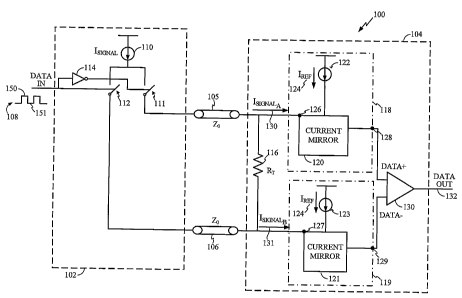
[0005] Figure 1 is a block diagram of a current mode transceiver interface
according to
an embodiment.
[0006] Figure 2 is a schematic diagram of one implementation of the current
mode
transceiver interface of Figure 1.
[0007] Figures 3A-C are plots showing results of simulations performed using
the
current mode transceiver interface of Figure 2.
[0008] Figure 4 shows a mobile phone including a current mode transceiver
interface
according to an embodiment.
DETAILED DESCRIPTION
[0009] Figure 1 shows a current mode transceiver interface 100 according to an
embodiment. The interface includes a driver 102, included on the transmitting
chip, a
receive block 104, included on the receiving chip, and dual transmission lines
105, 106.
Each chip may include both a driver and a receiver block for bi-directional
data transfer
between the chips. Also, multiple interfaces may be used to transfer data in
parallel
between chips.
[0010] The driver 102 receives an input data pattern 108 for transmission.
Current
mode differential signaling over the two transmission lines 105, 106 is used.
Based on a
voltage level of the input data 108, e.g., a HIGH voltage signal 150
(corresponding to
logic "1") or LOW voltage signal (corresponding to logic "0"), a current pulse
provided
by a current source 110 is sent over one of the transmission lines. Switches
111, 112
control which transmission line, 105 or 106, respectively, the current pulse
is sent over.
In an embodiment, each switch 111, 112 may be closed in response to a LOW
voltage
signal and opened for a HIGH voltage signal, with the input to switch 111
being
inverted by an inverter 114. Thus, for a HIGH voltage signal 150 (logic "1")
in the
input data 108, switch 111 is closed and switch 112 is open, allowing the
current pulse
to travel over transmission line 105, and for a LOW voltage signal 151 (logic
"0") in the
CA 02601453 2007-09-18
WO 2006/102666 PCT/US2006/011173
3
input data pattern 108, switch 112 is closed and switch 111 is opened,
transmitting the
current pulse over transmission line 106.
[0011] The transmission lines 105, 106 may each have a characteristic
impedance of 50
ohms, which is a common impedance value for most low cost transmission media.
Both
transmission lines are terminated by a resistor 116 at the receiving end. The
resistor 116
has a value, e.g., 100 ohms, selected to provide an appropriate receiver end
termination.
This resistor 116 and current mirror devices 120, 121 determine receiving end
impedance.
[0012] In the receiving block 104, current comparators 118, 119 may be used to
determine which transmission line the current was sent over. Each current
comparator
118, 119 may include a current mirror 120, 121 and a reference current Iref
source 122,
123, which may be less than 1 mA. In this type of current comparator, when the
input
current Isigõal at the input node 126 or 127 is greater than the reference
current Irefa the
voltage at the output nodes 128, 129, respectively, will drop to LOW.
Otherwise, the
node stays HIGH.
[0013] When a current pulse is sent over one of the transmission lines 105 or
106, the
two current mirrors 120, 121 will have different currents in them, IsigaatA
130 and IsignalB
131, respectively. These differential currents are mirrored with some gain K
(if
necessary) and these mirrored currents, K*IsigaalA and K*Isipa1B, are compared
against
the reference current Iref 124 supplied through the corresponding current
source 122,
123. This will produce a differential voltage, DATA+ and DATA-, at the output
nodes
128, 129 of the current comparators 118, 119. A cascode op-amp receiver 130
then
senses the differential voltage and produces the rail to rail single ended
output voltage,
DATA OUT 132.
[0014] Figure 2 is a schematic diagram of an exemplary embodiment of interface
100 in
which switches 111, 112 are PMOS transistors, current mirrors 120, 121 are
diode
configured NMOS current mirrors, and reference current sources 110, 122, 123
are
obtained from bias generator circuit. An exemplary data transmission will be
described
to illustrate operation of the interface 100 shown in Figure 2. When input
data 108 at
the driver transitions HIGH 150, the HIGH voltage signal will cause switch 112
to open,
and being inverted to a LOW voltage signal by inverter 114, cause MOS switch
111 to
close. A current pulse from current source 110 will be transmitted over
transmission
line 105. A majority of the transmitted current will be input to current
mirror 120 as
CA 02601453 2007-09-18
WO 2006/102666 PCT/US2006/011173
4
Is;gõ,IA 130. A small amount of current will cross resistor 116 and enter the
other current
mirror 121 as Is;pa1B 131. However, open switch 112 at the driver will prevent
any of
the current crossing resistor 116 from traveling across the other transmission
line 106.
This differs from other differential techniques such as LVDS, which include a
return
current path, i.e., current is returned across the non-transmitting line.
[0015] Reference current Iref 124 from reference current sources 122 and 123
is selected
to be below K*Is;,al of the transmitting line (in this case transmission line
105) and
above K*Is;pal of the non-transmitting line (in this case transmission line
106). In
current comparator 118, K*Isig,ai > Iref, causing node 128 (DATA+) to drop
LOW. In
current comparator 119, K*Is;gõa1 < Iref, causing node 129 (DATA-) to
transition HIGH.
The cascode op-amp receiver 130 senses the difference between the two voltages
and
outputs a LOW voltage signal, mirroring the LOW value at input data 108.
[0016] Figures 3A-C are plots showing the results of a simulation of the
operation of a
current mode transceiver interface according to an embodiment. Figure 3A shows
the
input data pattern 300 at the driver, which is reproduced accurately by the
output data
302 at the receive block, as shown in Figure 3B. Figure 3C shows the
corresponding
voltages 304, 306 at the output nodes (DATA+ 128, DATA- 129) of the current
comparators in the receive block. In this simulation, the differential swing
between
DATA+ 128, DATA- 129 is 21 mV. However, this swing could be made higher by
choosing higher value for Iref. The differential swing at nodes 126 and 127
could be
made as low as 10 to 15 mV, which is significantly lower than typical voltage
mode
techniques (e.g., -200mV). Also, the far end termination impedance could be
loosely
defined and the source termination at the driver could be used for proper
termination of
the transmission line.
[0017] Since the interface 100 uses true current mode signaling, it has very
high noise
immunity (typically most of the noise in chips is voltage mode). Also, the
point at
which current-to-voltage conversion is made in the receive block 104, i.e.,
nodes 128
and 129, has very low capacitance (mainly gate capacitance), which helps in
improving
slew rate (I/C) with the same low current. In an embodiment, the interface can
achieve
high data throughput with current consumption less than 1 mA, which is
significantly
lower than the typical 3.5 mA used in conventional LVDS techniques. Other
advantages
include order of magnitude savings in power over voltage mode techniques, a
high noise
margin facilitating a robust design, and reduced EMI injection.
CA 02601453 2007-09-18
WO 2006/102666 PCT/US2006/011173
[0018] The current mode interface transceiver may be used in a variety of
applications.
For example, Figure 4 shows a mobile phone 400 including a current mode
transceiver
interface for communicating data between a processor 402 and a display
controller 404
for a liquid crystal display (LCD) 406 (internal elements shown with dashed
lines). A
driver 408 on the processor 402 transmits data to a receive block 410 on the
display
controller 404 across transmit lines 412. As described above, each chip may
include
both a driver and a receiver block for bi-directional data transfer, and
multiple interfaces
may be used to transfer data in parallel between chips.
[0019] A number of embodiments have been described. Nevertheless, it will be
understood that various modifications may be made without departing from the
spirit
and scope of the invention. Accordingly, other embodiments are within the
scope of the
following claims.
[0020] What is claimed is: