Note: Descriptions are shown in the official language in which they were submitted.
CA 02601621 2015-01-16
- 54106-157
- 1 -
Description
Motor starter
The invention relates to a motor starter having a power
semiconductor switch, having an electricomechanical bypass
switch connected in parallel with it, and having control
electronics for driving the bypass switch.
Motor starters such as these are also referred to as "soft
starters". In a motor starter such as this the motor is
connected during a starting phase by the power semiconductor
switch which, for example, is in the form of a thyristor, while
the parallel bypass switch is open. In this case, the starting
power for the motor is continuously and gradually increased, in
particular in a regulated form, by appropriately driving the
power semiconductor switch, such that the motor starts "softly"
rather than suddenly. During operation of the motor, the power
semiconductor switches that are normally used would, however,
disadvantageously result in a comparatively high power loss. In
order to avoid this power loss, once the starting phase has
been completed, the supply current for the motor is no longer
passed via the power semiconductor switch but via the bypass
switch, whose losses are, considerably less, because it is a
mechanical switching element. A conventional electromechanical
switching unit is normally used as the bypass switch and
generally has a magnetic operating unit in order to operate the
actual mechanical switching element. The bypass switch is
driven by control electronics which are accommodated in the so-
called printed circuit board assembly. The printed circuit
board assembly is normally mounted above or alongside the
bypass switch and makes contact with the bypass switch by means
of essentially free wire lines. The lines are, for example,
soldered by appropriate connections to the printed circuit
board assembly, and make contact with the bypass switch by
means of a plug connection.
CA 02601621 2015-01-16
, 54106-157
- 2 -
This conventional solution is on the one hand comparatively
space-consuming, in particular because sufficient free space
must be provided for the lines in the enclosure of the motor
starter. The contact between the printed circuit board assembly
and the bypass switch furthermore involves a comparatively high
degree of installation and material complexity. Furthermore,
the lines which are essentially loose in the installed state
and therefore to a certain extent hang in the appliance in an
uncontrolled manner result in a certain risk of interference,
in terms of electromagnetic compatibility (EMV) and likewise a
certain risk of malfunction as a result of incorrectly
connected lines or an incorrect plug contact.
The invention is based on the object of improving a motor
starter of the type mentioned initially, against the background
described above.
According to the invention, this object is achieved by a motor
starter comprising a power semiconductor switch, comprising an
electromechanical bypass switch connected in parallel with it
and having control electronics for driving the bypass switch,
with the control electronics being in the form of a printed
circuit board assembly which is fixed to the bypass switch in
an installed state, with the printed circuit board assembly and
the bypass switch being designed such that, when being fixed,
the printed circuit board assembly makes electrical contact
with the bypass switch at the same time, and with the printed
circuit board assembly having at least two printed circuit
board sides forming a U-shaped hollow form or a hollow form in
the form of a trough, in whose interior the operating unit,
comprising a magnet coil and a magnet yoke, being located
between the at least two printed circuit board sides in the
CA 02601621 2015-01-16
54106-157
- 2a -
installed state, and facing electronic components on the
painted circuit boards.
This motor starter provides for the printed circuit board
assembly and the bypass switch to be designed such that they
are fixed to one another in an installed state, with the
printed circuit board assembly making electrical contact with
the bypass switch at the same time during fixing.
The fixing between the printed circuit board assembly and the
bypass switch is preferably designed such that the printed
circuit board assembly and the bypass switch form a cohesive,
essentially rigid component in the installed state, which
cannot be disconnected again, or can be disconnected only by
the application of force. The printed circuit board assembly is
in this case preferably connected to the bypass switch by a
snap-action connection, although other types of attachment,
such as screw connection, adhesive bonding, welding etc., can
also be used.
The expression fixing for the purposes of the invention can,
however, also be understood just as fixing the position of the
CA 02601621 2015-01-16
. 54106-157
- 3 -
printed circuit board assembly and the bypass switch with
respect to one another in such a manner that, when the motor
starter is assembled correctly, it is fixed or locked by other
components of the motor starter, in particular an enclosure of
it.
One essential feature of both variants for the purposes of the
invention is that the printed circuit board assembly and the
bypass switch are arranged in a well-defined position with
respect to one another in the installed state, and that, as a
consequence of this positioning, the printed circuit board
assembly makes electrical contact with the bypass switch at the
same time. This avoids the lines which are normally required
for the printed circuit board assembly to make contact with the
bypass switch, together with any plug contacts and solder
contacts, avoiding all of the disadvantages that are normally
associated with them.
In one preferred embodiment, the bypass switch is formed by a
mechanical switching element and an operating unit, in
particular a magnetic operating unit, for operating it. In one
particularly space-saving variant of the invention the printed
circuit board assembly is in this case expediently designed as
a U-shaped hollow form of a hollow form in the form of a
trough, which is placed on the operating unit in the installed
state so that the operating unit is held in the interior of the
hollow form. In addition to saving space, this embodiment has,
in particular, the further advantages that it makes it possible
to achieve particularly short electrical distances within the
circuit formed by the printed circuit board assembly and the
operating unit, thus on the one hand making it easier for the
printed circuit board assembly to make contact with the bypass
switch without the use of lines, while, on the hand, this is
advantageous from the EMV aspect. Furthermore, the operating
unit and the inner surface of the printed circuit board
assembly are in this way effectively shielded by the outer wall
of the printed circuit board assembly against mechanical
CA 02601621 2015-01-16
. 54106-157
- 4 -
damage, in particular in the course of the manufacturing
process. In particular, mechanically sensitive electronic
components of the printed circuit board assembly are mounted in
a preferred manner on its inner surface, by exploiting this
shielding effect.
In the installed position, the printed circuit board assembly
is expediently fixed to the operating unit of the bypass
switch, and in particular in the immediate vicinity of the
contact-making points there. This results in a particularly
robust and fail-safe electrical contact being made. In
particular, the fixing of the printed circuit board assembly to
the operating unit is also advantageous when the operating unit
of the bypass switch can be disconnected from the actual
switching element. In this case, the operating unit and the
printed circuit board assembly can first of all be connected
and have contact made between them separately in the course of
the installation process, being fitted as one component to the
switching element only during a subsequent manufacturing step,
which is advantageous from a production-engineering point of
view.
At least one spring contact is preferably provided in order to
make contact between the printed circuit board assembly and the
bypass switch, in particular with its operating unit, in a
manner which can be achieved easily from the production-
engineering point of view, costs little and is fail-safe.
In order to make it easier not only to populate the printed
circuit board assembly with electronic components but also to
fit the printed circuit board assembly to the bypass switch,
the printed circuit board assembly is expediently designed to
be flexible. In one preferred embodiment, the printed circuit
board assembly is provided with nominal bending points, in
particular in the form of film hinges, about which the printed
circuit board assembly can be bent without being destroyed.
Alternatively or additionally, the printed _circuit board
CA 02601621 2015-01-16
. 54106-157
- 5 -
assembly may optionally also be composed of a plurality of
pieces.
One exemplary embodiment of the invention will be explained in
more detail in the following text with reference to a drawing,
in which:
Figure 1 shows a schematic perspective view of a motor starter
with a power semiconductor switch, an
electromechanical bypass switch connected in parallel
with it, and with a printed circuit board assembly
which contains control electronics for driving the
bypass switch,
Figure 2 shows a perspective illustration, rotated with
respect to that shown in figure 1, of the bypass
switch for the motor starter with a mechanical
switching element and an electromechanical operating
unit,
Figure 3 shows a perspective illustration, once again rotated,
of the operating unit of the bypass switch with a
printed circuit board of the printed circuit board
assembly mounted on it,
Figure 4 shows a perspective illustration, once again rotated,
of the operating unit and of the printed circuit
board, which is now populated with electronic
components, of the printed circuit board assembly,
and
Figure 5 shows an enlarged detail v from figure 1 of a spring
contact for making contact between the printed
circuit board assembly and the bypass switch element.
Mutually corresponding parts are always provided with the same
reference symbols in all of the figures.
CA 02601621 2015-01-16
54106-157
- 6 -
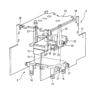
The motor starter 1 illustrated in Figure 1 has a power
semiconductor switch 2, in particular a thyristor. The motor '
starter 1 also has an electromechanical bypass switch 3, which
is connected in parallel with the power semiconductor switch 2,
and a printed circuit board assembly 4, which is fitted with
control electronics 5 for driving the bypass switch 4.
The power semiconductor switch 2, the bypass switch 3 and the
printed circuit board assembly 4 are accommodated in a common
enclosure 6, which is indicated just by outlines in Figure 1,
in the installed state as shown in Figure 1. In the installed
state, only connecting contacts 7 and 7' for connection of a
drive power line for a motor (not illustrated) project out of
the enclosure 6.
In the embodiment shown in Figure 1, the motor starter 1 is
designed to be connected in a drive power line (which in this
case by way of example has two phases) for a motor. In a
corresponding manner, the motor starter 1 has in each case one
pair of connecting contacts 7 and 7' for each of the two phase
lines, which project on opposite sides out of the enclosure 6
and can be respectively connected to the mains-side part and to
a motor-side part of the drive power line.
Internally, the power semiconductor 2 and the bypass switch 3
are connected internally in parallel between the associated
connecting contacts 7, 7'.
When being used correctly, the motor starter 1 is connected
upstream of the electrically powered motor in the drive power
line and is used for switching the motor on and off. The motor
starter 1 is in this case so-called soft starter, in which the
motor power is increased gradually, in particular in a
regulated manner, during a motor starting phase. In this
starting phase, the bypass switch 3 is open, and the motor is
therefore connected to the mains only by the power
CA 02601621 2015-01-16
54106-157
- 7 -
semiconductor switch 2. The gradual, in particular regulated,
increase in the motor power is in this case achieved by ,
appropriately driving the power semiconductor switch 2. In
order to save the power loss which is incurred across the power
semiconductor switch 2 during operation of the motor, the
bypass switch 3 is closed once the starting phase has ended,
and the power semiconductor switch 2 is therefore bridged, so
that the drive current for the motor flows via the bypass
switch 3, with low losses.
The bypass switch 3, which is illustrated separately once again
in Figure 2, for the motor starter 1 has a mechanical switching
element 8, which can be switched by means of an electromagnetic
operating unit 9.
For each phase line, the switching element 8 has in each case
one pair of mutually opposite fixed contacts 10, 10', each of
which is electrically connected to a corresponding connecting
contact 7 or 7', respectively. The fixed contacts 10 and 10' of
the same phase line can each be electrically reversibly
connected and disconnected via a moving contact link 11.
All of the contact links 11 are connected to a common plunger
12 and are always operated jointly by movement of the plunger
12. The plunger 12 is prestressed by a spring (which is not
illustrated in any more detail) such that the contact links 11
are locked in an open position, as illustrated in figure 2, in
the rest state, in which the connecting contacts 7, 7' of each
phase line are electrically disconnected from one another.
The operating unit 9 has a magnet coil 13 and a magnet yoke 14,
which form a magnetic circuit with a magnet armature 15. The
magnet armature 15 is in this case attached to the plunger 12
and therefore, from the physical point of view, forms a
component of the switching element 8. The components of the
operating unit 9, that is to say in particular the magnet coil
13 and the magnet yoke 14, are combined to form a cohesive and
CA 02601621 2015-01-16
54106-157
- 8 -
essentially rigid assembly, which is attached to the switching
element 8 by means of a snap-action connection 16.
In the installed state, a magnetic field is produced in the
magnetic circuit by application of a voltage to the magnet coil
13. Under the influence of this magnetic field, the magnet
armature 15 is attracted to the magnet yoke 14 and, during this
process, the contact links 11 are moved via the plunger 12
against the spring pressure from the open position to a closed
position, in which the mutually associated fixed contacts 10,
10' of each phase line are electrically conductively connected
to one another via the contact link 11.
The printed circuit board assembly 4, which is shown separately
in figures 3 and 4 together with the operating unit 9, is
formed essentially from a printed circuit board 17 with
electronic components 18 mounted on it, which are connected to
form the control electronics 5. Figure 3 in this case shows the
unpopulated printed circuit board 17, for the sake of clarity.
The printed circuit board 17 populated with the components 18
is shown in figure 4.
As can be seen from the illustrations, the printed circuit
board 17 is bent in the installed state to form a hollow shape
which essentially has a U-shaped cross section and holds the
operating unit 9 in its interior. The electronic components 18
of the printed circuit board assembly 4 are in this case
predominantly mounted on the inner surface of the printed
circuit board 17, facing the operating unit 9. On the one hand,
this has the advantage that the space available in the interior
of the printed circuit board 17 that is not occupied by the
operating unit 9 is made particularly good use of, and that, on
the other hand, the components 18 are well shielded from the
exterior and are therefore protected against mechanical damage,
for example during the installation process.
CA 02601621 2015-01-16
54106-157
- 9 -
As can be seen from figure 4 relatively small (printed circuit
board) attachments 19 are plugged onto the end faces of the, ,
printed circuit board 17 and partially cover the end surfaces
of the printed circuit board 17. The attachments 19 may be
fitted with further electronic components 18 and therefore
enlarge the useful area of the printed circuit board 17 that is
available for fitting the control electronics 5. It also offers
additional protection for the control electronics 5 and for the
operating unit 9 against mechanical damage.
As can be seen from figures 3 and 4, the printed circuit board
17 is fixed to the operating unit 9 by means of snap-action
connections 20, 21, so that the printed circuit board assembly
4 and the operating unit 9 form an assembly which is cohesive
in a self-supporting manner and is essentially rigid. The
mechanical robustness of this assembly is improved by two
supporting arms 22, which project from the operating unit 9 and
are supported at the free end on a cover 23 for the printed
circuit board 17.
As can be seen in particular from figure 5, which shows an
enlarged detailed illustration from figure 1 and figure 2,
contact is made between the printed circuit board assembly 4
and the operating unit 9 via two spring contacts 24. Each
spring contact 24 has a compression spring 25 composed of
electrically conductive material, which is pushed onto a guide
pin 26 which projects from the operating unit 9. The
compression spring 25 is in this case preferably clamped onto
the guide pin 26 and is thus held captive on the operating unit
9. Each guide pin 26 internally makes contact with a coil
connection 27 of the magnet coil 13.
In order to simplify the assembly of the motor starter 1, the
printed circuit board 17 is provided with flexible nominal
folding points 28 in the form of film hinges, which make it
possible to bend the printed circuit board 17 from its
originally flat state to the U-shape that can be seen in
CA 02601621 2015-01-16
. 54106-157
- 10 -
figures 3 and 4, without destroying it. The printed circuit /
board 17 is expediently populated with the electronic
components 18 when in the flat state. The complete printed
circuit board assembly 4 is then snapped onto the operating
unit 9, and is folded to the said U-shape during this process.
In this case, the printed circuit board 17 is provided on its
inner surface with conductive contact pads 29 which are
arranged such that the compression spring 25 of each spring
contact 24 is pressed against one of the contact pads 29 while
the printed circuit board 17 is being snapped on. This means
that the printed circuit board assembly 4 makes contact with
the operating unit 9 at the same time when the printed circuit
board 17 is being snapped onto the operating unit 9.
Once the printed circuit board assembly 4 has been snapped onto
the operating unit 9, the assembly that is formed in this way
is snapped onto the switching element 8, and the bypass switch
3, that is completed in this way, is connected to the power
semiconductor switch 2.
Overall, this results in a motor starter 1 which cannot only be
produced easily but is also compact and saves material, and
which furthermore is better than conventional motor starters of
the type mentioned initially both with respect to EMC criteria
and with respect to fail-safety.