Note: Descriptions are shown in the official language in which they were submitted.
CA 02602587 2007-09-26
WO 2006/107619 PCT/US2006/010787
1
MULTIPLEX FLUORESCENCE DETECTION DEVICE
HAVING REMOVABLE OPTICAL MODULES
TECHNICAL FIELD
The invention relates to assaying systems and, more particularly, techniques
for
the detection of multiple target species using fluorescent dyes.
BACKGROUND
Optical disc systems are often used to perform various biological, chemical or
bio-chemical assays. In a typical system, a rotatable disc is used as a medium
for
storing and processing fluid specimens, such as blood, plasma, serum, urine or
other
fluid.
One type of analysis is polymerase chain reaction (PCR), which is often used
for nucleic acid sequence analysis. In particular, PCR is often used for DNA
sequencing, cloning, genetic mapping, and other forms of nucleic acid sequence
analysis.
In general, PCR relies on the ability of DNA-copying enzymes to remain stable
at high temperatures. There are three major steps in PCR: denaturation,
annealing, and
extension. During the denaturation, a liquid sample is heated at approximately
94 C.
During this process, double DNA strands "melt" open into single stranded DNA
and all
enzymatic reactions stop. During annealing, the single stranded DNA is cooled
to
54 C. At this temperature, primers bind or "anneal" to the ends of the DNA
strands.
During extension, the sample is heated to 75 C. At this temperature,
nucleotides add to
the primers and eventually a complementary copy of the DNA template is formed.
There are a number of existing PCR instruments designed to determine levels of
specific DNA and RNA sequences in the sample during the PCR in real-time. Many
of
the instruments are based on the use of fluorescent dyes. In particular, many
conventional real-time PCR instruments detect a fluorescent signal produced
proportionally during amplification of a PCR product.
Conventional real-time PCR instruments use different methods for detection of
different fluorescent dyes. For example, some conventional PCR instruments
incorporate white light sources with filter wheels for spectrally resolving
each dye. The
white light sources are tungsten halogen bulbs, which have a lifetime maxima
of a few
CA 02602587 2007-09-26
WO 2006/107619 PCT/US2006/010787
2
thousand hours. The filter wheels are typically complicated electromechanical
parts that
are susceptible to wear.
SUMMARY
In general, the invention relates to techniques for the detection of multiple
target
species in real-time PCR (polymerase chain reaction), referred to herein as
multiplex
PCR. In particular, a multiplex fluorescence detection device is described
that
incorporates a plurality of optical modules. Each of the optical modules may
be
optimized for detection of a respective fluorescent dye at a discrete
wavelength band.
In other words, the optical modules may be used to interrogate multiple,
parallel
reactions at different wavelengths. The reaction may, for example, occur
within a
single process chamber (e.g., well) of a rotating disk. Additionally, each
optical
module may be removable to quickly change the detection capabilities of the
device.
The plurality of optical modules may be optically coupled to a single detector
by a multi-legged optical fiber bundle. In this manner, multiplexing can be
achieved by
using a plurality of optical modules and a single detector, e.g., a
photomultiplier tube.
The optical components in each optical module may be selected to maximize
sensitivity
and minimize the amount of spectral crosstalk, i.e., signals from one dye on
another
optical module.
In one embodiment, a device comprises a motor to rotate a disk having a
plurality of process chambers each holding a respective sample and a plurality
of
fluorescent dyes, a plurality of optical modules, and a housing having a
plurality of
locations adapted to receive the optical modules wherein each of the optical
modules
includes an optical channel having a light source selected for a different one
of the dyes
and a lens to capture fluorescent light emitted from the disk.
In another embodiment, a system comprises a data acquisition device. The
system further comprises a detection device coupled to the data acquisition
device,
wherein the detection device comprises a motor to rotate a disk having a
plurality of
process chambers each holding a respective sample and a plurality of
fluorescent dyes,
a plurality of optical modules, and a housing having a plurality of locations
adapted to
receive the optical modules wherein each of the optical modules includes an
optical
channel having a light source selected for a different one of the dyes and a
lens to
capture fluorescent light emitted from the disk.
CA 02602587 2007-09-26
WO 2006/107619 PCT/US2006/010787
3
In an additional embodiment, a method comprises rotating a disk having a
plurality of process chambers each having a plurality of species that emit
fluorescent
light at different wavelengths, exciting the disk with a plurality of light
beams to
produce a plurality of emitted fluorescent light beams, capturing the
fluorescent light
beams with a plurality of different optical modules, wherein the modules are
optically
configured for the different wavelengths, containing the plurality of
different modules
within a housing.
The invention may provide one or more advantages. For example, the modular
design may allow a technician to quickly and efficiently interchange detection
modules
depending on the particular reactions being performed. Moreover, the
technician may
select detection modules that are optically optimized for different reactions.
Further,
different combinations of detection modules may be installed and utilized
within the
real-time, multiplex PCR device.
While the device may be capable of conducting real-time PCR, the device may
be capable of analyzing any type of biological reaction while it occurs. The
device may
be able to modulate the temperature of each reaction independently or as a
selected
group, and the device may be able to support multiple stages of reactions by
including a
valve between two chambers. This valve may be opened during reactions through
the
use of a laser which delivers a burst of energy to the valve.
In some embodiments, the device may be portable and robust to allow operation
in remote areas or temporary laboratories. The device may include a data
acquisition
computer for analyzing the reactions in real-time, or the device may
communicate the
data to another device through wired or wireless communication interfaces.
The details of one or more embodiments of the invention are set forth in the
accompanying drawings and the description below. Other features, objects, and
advantages of the invention will be apparent from the description and
drawings, and
from the claims.
BRIEF DESCRIPTION OF DRAWINGS
FIG. 1 is a block diagram illustrating an exemplary embodiment of a multiplex
fluorescence detection device.
CA 02602587 2007-09-26
WO 2006/107619 PCT/US2006/010787
4
FIG. 2 is a schematic diagram illustrating an exemplary detection module,
which may correspond to any of a plurality of detection modules of the
fluorescence
detection device of FIG. 1.
FIG. 3 is a perspective diagram illustrating a front view of an exemplary set
of
removable optical modules within the device housing.
FIG. 4 is a perspective diagram illustrating the exemplary set of removable
optical modules within the device housing.
FIG. 5 is a perspective diagram illustrating a front side view of an exemplary
set
of removable optical modules having one module removed to expose a module
connector.
FIGS. 6A and 6B are perspective diagrams illustrating the components within
exemplary main removable optical modules.
FIGS. 7A and 7B are perspective diagrams illustrating the components within
exemplary supplemental removable optical modules.
FIG. 8 is a block diagram illustrating an example embodiment of the multiplex
fluorescence detection device in further detail.
FIG. 9 is a block diagram of the a single detector coupled to four optical
fibers
of the optical fiber bundle.
FIG. 10 is a flow diagram illustrating exemplary operation of the multiplex
fluorescence detection device.
FIG. 11 is a flow diagram illustrating an exemplary method if detecting light
and sampling data from the disk.
FIGS. 12 and 13 show the absorption and emission spectra of commonly used
fluorescent dyes that may be utilized for multiplex PCR.
FIGS. 14A and 14B illustrate raw data acquired from two exemplary detection
modules with a single detector during a PCR analysis.
FIG. 15 is a graph that shows the data once adjusted for a time offset.
FIGS. 16A and 16B show a limit of detection (LOD) for the data received from
two exemplary detection modules.
FIG. 17 is an exemplary screen shot of a temperature control user interface.
FIG. 18 is an exemplary screen shot of an optical control user interface.
FIG. 19 is an exemplary screen shot of a real-time PCR user interface.
CA 02602587 2007-09-26
WO 2006/107619 PCT/US2006/010787
DETAILED DESCRIPTION
FIG. 1 is a block diagram illustrating an exemplary embodiment of a multiplex
fluorescence detection device 10. In the illustrated example, device 10 has
four optical
modules 16 that provide four "channels" for optical detection of four
different dyes. In
5 particular, device 10 has four optical modules 16 that excite different
regions of
rotating disk 13 at any given time, and collect emitted fluorescent light
energy at
different wavelengths from the dyes. As a result, modules 16 may be used to
interrogate multiple, parallel reactions occurring within sample 22.
The multiple reactions may, for example, occur simultaneously within a single
chamber of a rotating disk 13. Each of optical modules 16 interrogates sample
22 and
collects fluorescent light energy at different wavelengths as the disk 13
rotates. For
example, excitation sources within modules 16 may be sequentially activated
for
periods sufficient to collect data at the corresponding wavelengths. That is,
an optical
module 16A may be activated for a period of time to collect data at a first
range of
wavelengths selected for a first dye corresponding to a first reaction. The
excitation
source may then be deactivated, and an excitation source within module 16B may
be
activated to interrogate sample 22 at a second range of wavelengths selected
for a
second dye corresponding to a second reaction. This process continues until
data has
been captured from all optical modules 16. In one embodiment, each of the
excitation
sources within optical modules 16 is activated for an initial period of
approximately
two seconds to reach steady state followed by an interrogation period which
lasts for
10-50 rotations of disk 13. In other embodiments, the excitation sources may
be
sequenced for shorter (e.g., 1 or 2 milliseconds) or longer periods. In some
embodiments, more than one optical module may be activated simultaneously for
concurrent interrogation of sample 22 without stopping the rotation of disk
13.
Although a single sample 22 is illustrated, disk 13 may contain a plurality of
chambers holding samples. Optical modules 16 may interrogate some or all of
the
different chambers at different wavelengths. In one embodiment, disk 13
includes 96
chambers space around a circumference of disk 13. With a 96 chamber disk and
four
optical modules 16, device 10 may be capable of acquiring data from 384
different
species.
In one embodiment, optical modules 16 include excitation sources that are
inexpensive high power light emitting diodes (LEDs), which are commercially
CA 02602587 2007-09-26
WO 2006/107619 PCT/US2006/010787
6
available in a variety of wavelengths and have long lifetimes (e.g., 100,000
hours or
more). In another embodiment, conventional halogen bulbs or mercury lamps may
be
used as excitation sources.
As illustrated in FIG. 1, each of optical modules 16 may be coupled to one leg
of a fiber optic bundle 14. Fiber optic bundle 14 provides a flexible
mechanism for
collection of fluorescent signals from optical modules 16 without loss of
sensitivity. In
general, a fiber optic bundle comprises multiple optical fibers laid side by
side and
bonded together at the ends and encased in a flexible protective jacket.
Alternatively,
fiber optic bundle 14 may comprise a smaller number of discrete, large
diameter multi-
mode fibers, either glass or plastic, having a common end. For example, for a
four-
optical module device, fiber optic bundle 16 may comprise four discrete
multimode
fibers, each having a 1 mm core diameter. The common end of the bundle
contains the
four fibers bound together. In this example, the aperture of detector 18 may
be 8 mm,
which is more than sufficient for coupling to the four fibers.
In this example, fiber optic bundle 14 couples optical modules 16 to a single
detector 18. The optical fibers carry the fluorescent light collected by
optical modules
16 and effectively deliver the captured light to detector 18. In one
embodiment,
detector 18 is a photomultiplier tube. In another embodiment, the detector may
include
multiple photomultiplier elements, one for each optical fiber, within the
single detector.
In other embodiments, one or more solid-state detectors may be used.
The use of a single detector 18 may be advantageous in that it allows use of a
highly sensitive and possibly expensive detector (e.g., a photomultiplier),
while
maintaining a minimal cost in that only a single detector need be used. A
single
detector is discussed herein; however, one or more detectors may be included
for
detecting a greater number of dyes. For example, four additional optical
modules 16
and a second detector may be added to the system to allow for the detection of
eight
different wavelengths emitted from one disk. An exemplary fiber optic bundle
coupled
to a single detector for use with rotating disk 13 is described in U.S. Patent
Application
Serial No. 11/174,755, entitled "MULTIPLEX FLUORESCENCE DETECTION
DEVICE HAVING FIBER BUNDLE COUPLING MULTIPLE OPTICAL
MODULES TO A COMMON DETECTOR," filed on July 5, 2005.
Optical modules 16 are removable from the device and easily interchangeable
with other optical modules that are optimized for interrogation at different
wavelengths.
CA 02602587 2007-09-26
WO 2006/107619 PCT/US2006/010787
7
For example, optical modules 16 may be physically mounted within locations of
a
module housing. Each of optical modules 16 may be easily inserted within a
respective
location of the housing along guides (e.g., recessed grooves) that mate with
one or
more marking (e.g., guide pins) of the optical module. Each optical module
includes an
optical output port (shown in FIGS. 6A and 7A) for coupling to one leg of
fiber optic
bundle 14. The optical output port may have a threaded end coupled to a
threaded
connector of the leg. Alternatively, a form of "quick-connect" may be used
(e.g., a
slidable connection having an o-ring and a catch pin) that allows fiber optic
bundle 14
to be slidably engaged and disengaged from the optical output port. Moreover,
each of
optical modules 16 may have one or more electrical contacts for electronically
coupling
to control unit 23 when fully inserted.
The modular architecture of device 10 allows the device to be easily adapted
for
all of the fluorescent dyes used in a given analysis environment, such as
multiplex
PCR. Other chemistries that may be used in device 10 include Invader (Third
Wave,
Madison, Wisconsin), Transcripted-mediated Amplification (GenProbe, San Diego,
California), fluorescence labeled enzyme linked immunosorbent assay (ELISA) or
fluorescence in situ hybridization (FISH). The modular architecture of device
10 may
provide another advantage in that the sensitivity of each optical module 16
can be
optimized by choice of the corresponding excitation source (not shown) and
excitation
and detection filters for a small specific target range of wavelengths in
order to
selectively excite and detect a corresponding dye in the multiplex reaction.
For purpose of example, device 10 is illustrated in a 4-color multiplex
arrangement, but more or less channels can be used with the appropriate fiber
optic
bundle 14. This modular design allows a user to easily upgrade device 10 in
the field
by simply adding another optical module 16 to base 20 and inserting one leg of
fiber
optic bundle 14 into the new optical module. Optical modules 16 may have
integrated
electronics that identify the optical modules and download calibration data
into an
internal control module or other internal electronics (e.g., control unit 23)
of device 10.
In the example of FIG. 1, samples 22 are contained in chambers of disk 13,
which is mounted on a rotating platform under the control of control unit 23.
A slot
sensor trigger 27 provides an output signal utilized by control unit 23 and
data
acquisition device 21 for synchronizing data acquisition with chamber position
during
disk rotation. Slot sensor trigger 27 may be a mechanical or optical sensor.
For
CA 02602587 2007-09-26
WO 2006/107619 PCT/US2006/010787
8
example, the sensor may be a laser which sends a beam of light to disk 13 and
control
unit 23 uses a sensor detecting light passing through a slot in disk 13 to
locate the
chambers on the disk. In other embodiments, disk 13 may include a tab,
protrusion or
reflective surface in addition to or in place of the slot. Slot sensor trigger
27 may use
any physical structure or mechanism to locate the radial position of disk 13
as it rotates.
Optical modules 16 may be physically mounted above rotating platform 25. As a
result, optical modules 16 are overlapped with different chambers at any one
time.
Detection device 10 also includes a heating element (not shown) for modulating
the temperature of the sample 22 on disk 13. The heating element may comprise
a
cylindrical halogen bulb contained within a reflective enclosure. The
reflective
chamber is shaped to focus radiation from the bulb onto a radial section of
disk 13.
Generally, the heated area of disk 13 would resemble a ring as disk 13 spins.
In this
embodiment, the shape of the reflective enclosure may be a combination of
elliptical
and spherical geometries that allow precise focusing. In other embodiments,
the
reflective enclosure may be of a different shape or the bulb may broadly
irradiate a
larger area. In other embodiments, the reflective enclosure may be shaped to
focus the
radiation from the bulb onto a single area of the disk 13, such as a single
process
chainber containing a sample 22.
In some embodiments, the heating element may heat air and force the hot air
over one or more samples to modulate the temperature. Additionally, the
samples may
be heated directly by the disk. In this case, the heating element may be
located in
platform 25 and thermally couple to disk 13. Electrical resistance within the
heating
element may heat a selected region of the disk as controlled by control unit
23. For
example, a region may contain one or more chambers, possibly the entire disk.
An
exemplary heating element for use with rotating disk 13 is described in U.S.
Patent
Application Serial No. 11/174,691, entitled "HEATING ELEMENT FOR A
ROTATING MULTIPLEX FLUORESCENCE DETECTION DEVICE," filed on
July 5, 2005.
Alternatively, or in addition, device 10 may also includes a cooling component
(not shown). A fan is included in device 10 to supply cold air, i.e., room
temperature
air, to disk 13. Cooling may be needed to modulate the temperature of the
sample
appropriately and store samples after an experiment has completed. In other
embodiments, the cooling component may include thermal coupling between
platform
CA 02602587 2007-09-26
WO 2006/107619 PCT/US2006/010787
9
25 and disk 13, as platform 25 may reduce its temperature when needed. For
example,
some biological samples may be stored at 4 degrees Celsius to reduce enzyme
activity
or protein denaturing.
Detection device 10 may also be capable of controlling reaction species
contained within a process chamber. For example, it may be beneficial to load
some
species in a process chamber to generate one reaction and later adding another
species
to the sample once the first reaction has terminated. A laser homing valve may
be
added to control a valve position separating an inner holding chamber from the
process
chamber, thereby controlling the addition of species to the chamber during
rotation of
disk 13. This laser device may be located within one of optical modules 16 or
separate
from the optical modules. Directly below the laser, under disk 13, may be a
laser
sensor for positioning the laser relative to disk 13.
In one embodiment, the laser is a near infrared (NIR) laser with at least two
power settings. Under a low power setting, the laser positioning sensor may
indicate
that the laser is in position over the chamber valve by recognizing the NIR
light though
a slot in disk 13. Once the laser is in position, control unit 23 directs the
laser to output
a short burst of high power energy to heat the valve and open it. The open
valve may
then allow the inner fluid specimen to flow toward from the inside chamber to
the
outside process chamber and conduct a second reaction. In some embodiments,
disk 13
may contain a plurality of valves to generate a plurality of reactions in
sequence. More
than one set of laser and laser sensor may also be used when utilizing
multiple chamber
valves. An exemplary laser homing valve control system for use with rotating
disk 13
is described in U.S. Patent Application Serial No. 11/174,957, entitled "VALVE
CONTROL SYSTEM FOR A ROTATING MULTIPLEX FLUORESCENCE
DETECTION DEVICE," filed on July 5, 2005.
Data acquisition device 21 may collect data from device 10 for each dye either
sequentially or in parallel. In one embodiment, data acquisition system 21
collects the
data from optical modules 16 in sequence, and corrects the spatial overlap by
a trigger
delay for each one of the optical modules measured from slot sensor trigger
27.
One application for device 10 is real-time PCR, but the techniques described
herein may be extended to other platforms that utilize fluorescence detection
at multiple
wavelengths. Device 10 may combine rapid thermal cycling, utilizing the
heating
element, and centrifugally driven microfluidics for isolation, amplification,
and
CA 02602587 2007-09-26
WO 2006/107619 PCT/US2006/010787
detection of nucleic acids. By making use of multiplex fluorescence detection,
multiple
target species may be detected and analyzed in parallel.
For real-time PCR, fluorescence is used to measure the amount of amplification
in one of three general techniques. The first technique is the use of a dye,
such as Sybr
5 Green (Molecular Probes, Eugene, Oregon), whose fluorescence increases upon
binding to double-stranded DNA. The second technique uses fluorescently
labeled
probes whose fluorescence changes when bound to the amplified target sequence
(hybridization probes, hairpin probes, etc.). This technique is similar to
using a double-
stranded DNA binding dye, but is more specific because the probe will bind
only to a
10 certain section of the target sequence. The third technique is the use of
hydrolysis
probes (TaqmanTM, Applied BioSystems, Foster City California), in which the
exonuclease activity of the polymerase enzyme cleaves a quencher molecule from
the
probe during the extension phase of PCR, making it fluorescently active.
In each of the approaches, fluorescence is linearly proportional to the
amplified
target concentration. Data acquisition system 21 measures an output signal
from
detector 18 (or alternatively optionally sampled and communicated by control
unit 23)
during the PCR reaction to observe the amplification in near real-time. In
multiplex
PCR, the multiple targets are labeled with different dyes that are measured
independently. Generally speaking, each dye will have different absorbance and
emission spectra. For this reason, optical modules 16 may have excitation
sources,
lenses and related filters that are optically selected for interrogation of
sample 22 at
different wavelengths.
Some examples of suitable construction techniques or materials that may be
adapted for use in connection with the present invention may be described in,
e.g.,
commonly-assigned U.S. Patent No. 6,734,401 titled "ENHANCED SAMPLE
PROCESSING DEVICES SYSTEMS AND METHODS" (Bedingham et al.) and U.S.
Patent Application Publication No. US 2002/0064885 titled "SAMPLE PROCESSING
DEVICES." Other useable device constructions may be found in, e.g., U.S.
Provisional
Patent Application Serial No. 60/214,508 filed on June 28, 2000 and entitled
"THERMAL PROCESSING DEVICES AND METHODS"; U.S. Provisional Patent
Application Serial No. 60/214,642 filed on June 28, 2000 and entitled "SAMPLE
PROCESSING DEVICES, SYSTEMS AND METHODS"; U.S. Provisional Patent
Application Serial No. 60/237,072 filed on October 2, 2000 and entitled
"SAMPLE
CA 02602587 2007-09-26
WO 2006/107619 PCT/US2006/010787
11
PROCESSING DEVICES, SYSTEMS AND METHODS"; U.S. Provisional Patent
Application Serial No. 60/260,063 filed on January 6, 2001 and titled "SAMPLE
PROCESSING DEVICES, SYSTEMS AND METHODS"; U.S. Provisional Patent
Application Serial No. 60/284,637 filed on April 18, 2001 and titled "ENHANCED
SAMPLE PROCESSING DEVICES, SYSTEMS AND METHODS"; and U.S. Patent
Application Publication No. US 2002/0048533 titled "SAMPLE PROCESSING
DEVICES AND CARRIERS." Other potential device constructions may be found in,
e.g., U.S. Patent No. 6,627,159 titled "CENTRIFUGAL FILLING OF SAMPLE
PROCESSING DEVICES" (Bedingham et al.).
FIG. 2 is a schematic diagram illustrating an exemplary optical module 16A,
which may correspond to any of optical modules 16 of FIG. 1. In this example,
optical
module 16A contains a high-power excitation source, LED 30, a collimating lens
32, an
excitation filter 34, a dichrotic filter 36, a focusing lens 38, a detection
filter 40, and a
lens 42 to focus the fluorescence into one leg of fiber optic bundle 14.
Consequently, the excitation light from LED 30 is collimated by collimating
lens 32, filtered by excitation filter 34, transmitted through dichrotic
filter 36, and
focused into the sample 22 by focusing lens 38. The resulting fluorescence
emitted by
the sample is collected by the same focusing lens 38, reflected off of
dichrotic filter 36,
and filtered by detection filter 40 before focused into one leg of fiber optic
bundle 14.
The optic bundle 14 then transfers the light to detector 18.
LED 30, collimating lens 32, excitation filter 34, dichrotic filter 36,
focusing
lens 38, detection filter 40, and lens 42 are selected based on the specific
absorption
and emission bands of the multiplex dye with which optical module 16A is to be
used.
In this manner, multiple optical modules 16 may be configured and loaded
within
device 10 to target different dyes.
Table 1 lists exemplary components that may be used in a 4-channel multiplex
fluorescence detection device 10 for a variety of fluorescent dyes. FAM, HEX,
JOE,
VIC, TET, ROX are trademarks of Applera, Norwalk, California. Tamra is a
trademark
of AnaSpec, San Jose, California. Texas Red is a trademark of Molecular
Probes. Cy 5
is a trademark of Amersham, Buckinghamshire, United Kingdom.
CA 02602587 2007-09-26
WO 2006/107619 PCT/US2006/010787
12
TABLE 1
Optical
Module LED Excitation Filter Detection Filter Dye
1 blue 475 nm 520 nm FAM, Sybr Green
2 green 530 nm 555 nm HEX, JOE, VIC, TET
3 orange 580 nm 610 nm TAMRA, ROX, Texas Red
4 red 630 nm 670 nm Cy 5
One advantage of the described modular, multiplex detection architecture is
the
flexibility in optimizing detection for a wide variety of dyes. Conceivably a
user may
have a bank of several different optical modules that can be plugged into
device 10 as
needed, of which N can used at any one time, where N is the maximum number of
channels supported by the device. Therefore, device 10 and optical modules 16
may be
used with any fluorescent dye and PCR detection method. A larger fiber optic
bundle
may be used to support a larger number of detection channels. Moreover,
multiple
fiber optic bundles may be used with multiple detectors. For example, two 4-
legged
fiber optic bundles may be used with eight optical modules 16 and two
detectors 18.
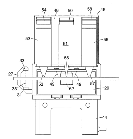
FIG. 3 is a perspective diagram illustrating a front view of an exemplary set
of
removable optical modules within the device housing. In the example of FIG. 3,
device
10 includes base ann 44 and module housing 46. Main optical module 48,
supplemental optical module 52 and supplemental optical module 56 are
contained
within module housing 46. Optical modules 48, 52 and 56 produce optical output
beams 49, 53 and 57, respectively, that sequentially excite different process
chambers
of disk 13. In other words, output beams 49, 53 and 57 follow the curvature of
disk 13
to each excite the same radial position of the disk which contains the process
chambers.
Slot sensor trigger 27 includes infrared light source 31 which produces light
35 that is
detected by detector 33.
Each of optical modules 48, 52 and 56 includes a respective release lever 50,
54
or 58, respectively, for engaging module housing 46. Each release lever may
provide
an upward bias to engage a respective latch formed within module housing 46. A
technician or other user depresses release levers 50, 54 or 58, respectively,
in order to
unlatch and remove optical module 48, 52 or 56 from module housing 46. Barcode
reader 29 includes laser 62 for identifying disk 13.
CA 02602587 2007-09-26
WO 2006/107619 PCT/US2006/010787
13
Base arm 44 extends from detection device 10 and provides support for module
housing 46 and optical modules 48, 52 and 56. Module housing 46 may be
securely
mounted atop base arm 44. Module housing 46 may contain a location adapted to
receive a respective one of optical modules 48, 52 and 56. Although described
for
exemplary purposes with respect to module housing 46, module housing 46 of
detection device 10 may have a plurality of locations for receiving optical
modules 48,
52 and 56. In other words, a separate housing need not be used for optical
modules 48,
52and56.
Each location of module housing 46 may contain one or more tracks or guides
which help to correctly position the associated optical module within the
location when
a technician or other user inserts the optical module. These guides may be
located
along the top, bottom, or sides of each locations. Each of optical modules 48,
52 and
56 may include guides or tracks that mate with the guides or tracks of the
locations of
module housing 46. For example, module housing 46 may have protruding guides
which mate with recessed guides in optical modules 48, 52 and 56.
In some embodiments, module housing 46 may not completely enclose each of
optical modules 48, 52 and 56. For example, module housing 46 may provide
mounting points to secure each of optical modules 48, 52 and 56 to base arm
44, but
portions or all of each optical module may be exposed. In other embodiments,
module
housing 46 may completely enclose each of optical modules 48, 52 and 56. For
example, module housing 46 may include a single door that closes over optical
modules
48, 52 and 56, or a respective door for each of the modules. This embodiment
may be
appropriate for applications where the modules are seldom removed or detection
device
10 is subjected to extreme environmental conditions.
A technician may easily remove any of optical modules 48, 52 or 56, and may
be completed by using only one hand. For example, the technician may rest his
or her
forefinger under a molded lip located beneath release lever 54 of optical
module 52.
The technician's thumb may then press down release lever 54 to release optical
module
52 from module housing 46. While grasping optical module 52 between the thumb
and
forefinger, the technician may pull back on the optical module to remove the
optical
module from detection device 10. Other methods may be used to remove any of
optical
module 48, 52 or 56, including methods utilizing two-handed removal. Inserting
any of
CA 02602587 2007-09-26
WO 2006/107619 PCT/US2006/010787
14
optical module 48, 52 or 56 may be accomplished in a reversed manner with one
or two
hands.
In the example of FIG. 3, the components of two optical modules are combined
to form main optical module 48. Main optical module 48 may contain light
sources
that produce two different wavelengths of light and detectors for detecting
each
different wavelength of fluorescence from the samples in disk 13. Therefore,
main
optical module 48 may connect to two legs of fiber optic bundle 14. In this
manner,
main optical module 48 may be viewed as a dual-channeled optical module having
two
independent optical excitation and collection channels. In some embodiments,
main
optical module 48 may contain optical components for more than two optical
modules.
In other cases, module housing 46 contains a plurality (e.g., two or more) of
single-
channeled optical modules, such as supplemental optical modules 52 and 56.
As illustrated in FIG. 3, main optical module 48 may also contain components
for a laser valve control system 51 (located within optical module 48). Laser
valve
control system 51 detects disk 13 location by a small slot located near the
outer edge of
disk 13. A detector (not shown) detects low power laser light 55 to map the
location of
disk 13 with respect to the motor which spins the disk. The control unit 23
uses the
map to locate valves (not shown) on disk 13.
Laser valve control system 51 focuses laser light 55 on the valves that
separate
holding chambers towards the center of disk 13 from process chambers near the
outer
edge of disk 13. When the contents of the holding chambers are to be moved to
the
associated process chambers, laser valve control system 51 applies laser light
55 to heat
a valve separating the chambers, causing the value open and providing fluid
communication between the two chambers. In particular, once the valve is open,
the
contents from the imler holding chamber may then flow towards the outer
process
chamber as disk 13 is spinning. Detection device 10 may then monitor the
subsequent
reaction in the process chamber. Contents within a chamber may include
substances in
a fluid or solid state.
In some embodiments, laser valve control system 51 may be contained within a
single-channeled optical module, e.g., supplemental optical module 54 or
supplemental
optical module 56. In other embodiments, laser valve control system 51 may be
mounted to detection device 10 separately from any of optical modules 48, 52
or 56. In
CA 02602587 2007-09-26
WO 2006/107619 PCT/US2006/010787
this case, laser valve control system 51 may be removable and adapted to
engage a
location within module housing 46 or a different housing of detection device
10.
In the example of FIG. 3, slot sensor trigger 27 is located near the removable
modules, on either side of disk 13. In one embodiment, slot sensor trigger 27
contains
5 a light source 31 to emit infrared (IR) light 35. Detector 33 detects IR
light 35 when
the slot in disk 13 allows the light to pass through the disk to detector 33.
Control unit
23 may use this information to synchronize disk 13 location as it is spinning
with data
from optical modules 48, 54 and 56. In some embodiments, slot sensor trigger
27 may
extend from base arm 44 to reach the outer edge of disk 13 during device 10
operation.
10 In other embodiments, a mechanical detector may be used to detect the
position of disk
13.
Barcode reader 29 uses laser 62 to read a barcode located on the side edge of
disk 13. The barcode identifies the type of disk 13 to allow proper operation
of device
10. In some embodiments, the barcode may identify the actual disk to assist a
15 technician in tracking data to specific samples from multiple disks 13.
All surface components of optical modules 48, 52 and 56 may be constructed of
a polymer, composite, or metal alloy. For example, high molecular weight
polyurethane may be used in forming the surface components. In other cases, an
aluminum alloy or carbon fiber structure may be created. In any case, the
material may
be resistant to heat, fatigue, stress, and corrosion. As detection device 10
may come
into contract with biological materials, the structures may be sterilizable in
the event
chamber contents leak out of disk 13.
FIG. 4 is an perspective diagram illustrating the exemplary set of removable
optical modules 48, 52 and 56 within module housing 46 of detection device 10.
In the
example of FIG. 4, base arm 44 supports barcode reader 29 as well as the
removable
optical modules 48, 52 and 56 attached within module housing 46. Disk 13 is
located
beneath optical modules 48, 52 and 56 with the process chambers located under
a
respective optical path of each of the modules at different moments in time.
Within module housing 46, the fronts of supplementary module 56 and main
optical module 48 can be seen. Supplementary module 56 contains molded lip 59
and
release lever 58. As previously described, molded lip 59 may be used to grasp
module
56 when removing or inserting the module into module housing 46. All of
optical
modules 48, 52 and 56 may have a respective molded lip and release lever, or a
single
CA 02602587 2007-09-26
WO 2006/107619 PCT/US2006/010787
16
release lever may be used to remove all of the optical modules. In some
embodiments,
optical modules 48, 52 and 56 may contain a different component for grasping
the
module. For example, each of optical modules 48, 52 and 56 may contain a
handle for
removing the respective module in a vertical or horizontal direction from
module
housing 46.
The location of optical modules 48, 52 and 56 within module housing 46 may
be fixed in order to separately excite different samples within disk 13 at any
particular
moment in time. For example, main optical module 48 may be located slightly
further
toward base arm 44 than supplemental optical modules 52 and 56, which are
offset to a
location at either side of the main module. Moreover, optical modules 48, 52
and 56
may be offset in a horizontal direction (indicated by the arrow in FIG. 4,
where X is the
distance the outside light beams are offset from the inside light beams) so
that the
excitation light beams produced by the modules follows the curvature of disk
13. In
this arrangement, the light beams produced by optical modules 48, 52 and 56
traverse
the same path as disk 13 rotates, thereby exciting and collecting light from
process
chambers located along the path. In other embodiments, optical modules 48, 52
and 56
are aligned such that the excitation light beams traverse different paths
around rotating
disk 13.
In this example, base arm 44 contains electrical contact board 66 which
extends
into module housing 46. Inside module housing 46, electrical contact board 66
may
contain electrical contacts for each of optical modules 48, 52 and 56.
Electrical contact
board 66 may be electrically coupled to control unit 23. In some embodiments,
each of
optical modules 48, 52 and 56 may have a separate associated electrical
contact board
which is connected to control unit 23.
Fiber optic coupler 68 couples one leg of the fiber optic bundle 14 to an
optical
output port of optical module 56. Although not shown, each of optical modules
48, 52
and 56 include an optical output port adapted to engage a respective fiber
optic coupler
mounted to module housing 46. The connection between fiber optic coupler 68
and the
leg of fiber optic bundle 14 may be a threaded screw lock, snap closure or
friction fit.
Barcode reader 29 produces laser liglzt 64 for reading the barcode of disk 13.
The laser light 64 follows a direct path where it interacts with the outer
edge of disk 13.
The light 64 may spread out to cover a large area of disk 13 at one time.
Barcode
reader 29 reads the barcode on disk 13 when the disk is rotating at slow
speeds. In
CA 02602587 2007-09-26
WO 2006/107619 PCT/US2006/010787
17
other embodiments, barcode reader 29 may read the barcode periodically during
operation to make sure a new disk has not been loaded in device 10. The
barcode
reader 29 may detect more than one barcode on disk 13 in other embodiments.
In some embodiments, base arm 44 may be movable with respect to disk 13. In
this case, base arm 44 could be configurable to detect samples on different
sized disks
or samples located within an interior of disk 13. For example, a larger disk
containing
more process chambers or larger process chambers may be used by moving the
base
arm 44 further away from the center of disk 13. Module housing 46 may also
have a
configurable position for each of optical module 48, 52 or 56 so that each
module may
be movable to one or more circular paths of process chambers around disk 13.
FIG. 5 is perspective diagram illustrating a front side view of an exemplary
set
of removable optical modules having one module removed to expose a module
connector. In particular, module housing 46 is not shown in FIG. 5, and
optical module
56 has been removed to expose optical modules 52 and 48 along with the
connections
for removed module 56.
Release lever 58 (FIG. 3) of optical module 56 securely attaches to attachment
post 69 mounted to base arm 44. In this example, attachment post 69 extends
into
optical module 56 and couples to release lever 58. In other embodiments, other
attachment mechanisms may be used to fix optical module 56 to base arm 44,
such as a
screw or snap fixation device.
Base arm 44 provides two different operational connections within module
housing 46 for receiving and engaging optical module 56, once inserted. In
particular,
base arm 44 provides electrical contact board 66, which includes electrical
connections
70 for coupling to the electrical contacts (not shown) contained within
optical module
56. Electrical connections 70 allow control unit 23 to communicate with
electrical
components within module 56. For example, module 56 may include electrical
circuits,
hardware, firmware, or any combination thereof. In one example, the internal
electrical components may store and output to control unit 23 unique
identification
information, such as a serial number. Alternatively, or in addition, the
electrical
components may provide information describing the specific characteristics of
the
optical components contained within the removable module 56. For example, the
electrical components may include programmable read-only memory (PROM), flash
memory, or other internal or removable storage media. Other embodiments may
CA 02602587 2007-09-26
WO 2006/107619 PCT/US2006/010787
18
include a set of resistors, a circuit or an imbedded processor for outputting
a unique
signature of optical modules 48, 52 or 56 to control unit 23. In another
example,
optical module 56 may include a laser source and other components that form
part of a
laser valve control system, i.e. laser valve control system 51.
Electrical contact board 66 may be removed and replaced with another version
associated with a different removable optical module. This option may support
upgrades in device capability. In other embodiments, connections 70 may
contain
more or less connection pins.
In addition, base arm 44 and module housing 46 provide optical channel 72
within the location for receiving optical module 56. Optical channel 72 is
connected to
fiber optic coupler 68 (FIG. 4) that interfaces with a leg of fiber optic
bundle 14.
Optical channel 72 inserts into a location within optical module 56. The light
captured
by optical module 56 may be directed through optical channel 72, fiber optic
coupler 68
and fiber optic bundle 15 to the detector. Fittings between these connections
may be
tight to ensure that light does not escape or enter the optical path.
In some embodiments, the connections to optical module 56 may be arranged in
a different configuration. For example, the connections may be located in
another
position for accepting optical module 56 from another direction. In other
embodiments,
electrical comzections may be located on one side of optical module 56 while
an
optical connection is located on a second surface of module 56. In any case,
the
electrical and optical connections located within the location of module
housing 46
accommodate a removable optical module, i.e., optical module 56 in this
example.
The optical and electrical connections of module 56 described in FIG. 5 may be
used with any module, including optical modules 48 and 52. In addition, the
connections for each optical module may not be identical. Since comiections
may be
modified for coupling with a desired removable optical module, the connections
utilized by any particular optical module inserted within a particular
location of module
housing 46 may vary at any time.
FIG. 6A is perspective diagram illustrating the components within an exemplary
main removable optical module 48A. In the example of FIG. 6A, main optical
module
48A includes release lever 50, pivot pin 51 and latch 74. Internal housing 78
separates
each side of module 48A and contains electrical contacts pad 80 connected to
ribbon
81. Optical components include LED 82, collimating lens 84, excitation filter
86,
CA 02602587 2007-09-26
WO 2006/107619 PCT/US2006/010787
19
dichrotic filter 88, focusing lens 90, detection filter 92 and lens 94.
Optical output port
17 couples to a leg of fiber optic bundle 14. A separate set of optical
components for a
second optical channel (not shown) are located on the other side of internal
housing 78.
In addition, main module 48A includes connector 96, laser diode 98 and
focusing lens
100 as part of a laser valve control system 51 controlled by control unit 23.
Release lever 50 is attached to optical module 48A by a pivot pin 61. Pivot
pin
61 allows release lever 50 to rotate about the axis of the pin. When release
lever 50 is
depressed, arm 63 rotates counter-clockwise to raise latch 74. Once latch 74
is raised,
optical module 48A may be free for removal from module housing 46. There may
be a
spring or other mechanism maintaining a bias force against release lever 50 to
maintain
latch 74 in a down position. In some embodiments, a spring may be included
around
pivot pin 61 to provide a moment arm that keeps latch 74 in the down, or
latched,
position. In other embodiments, other mounting mechanisms may be added to or
used
in place of the described lever. For example, optical module 48A may be
attached to
module housing 46 by one or more screws or pins.
Mounting board 76 may be installed within optical module 48A for attaching
communication ribbon 81 and LED 82. Ribbon 81 is connected to electrical
contacts
pad 80 and provides a connection between the pad and electrical components
within
optical module 48A. Contacts pad 80 and ribbon 81 may carry the information
required for both sides of main optical module 48A, including the laser valve
control
system 51 and any internal memory or other storage medium. Ribbon 81 may be
flexible for weaving within optical module 48A. Ribbon 81 may contain a
plurality of
electrically conductive wires to communicate signals between the electrical
components and control unit 23 and/or to deliver power to the electrical
components.
In some embodiments, each electrical component may have a separate cable
connecting
the component with control unit 23. A technician may need to disconnect a
cable or
flex circuit from module housing 46 when removing optical module 48A from the
housing.
In some embodiments, optical module 48A may contain a detector for detecting
light from disk 13 and electronics for processing and storing the data. The
electronics
may contain a telemetry circuit for wirelessly transmitting data representing
the
detected light to control unit 23. Wireless communication may be performed by
infrared light, radio frequency, Bluetooth, or other telemetry technique.
Optical
CA 02602587 2007-09-26
WO 2006/107619 PCT/US2006/010787
module 48A may also include a battery to power the electronics, which may be
rechargeable by control unit 23.
LED 82 is affixed to mounting board 76 and electrically coupled to ribbon 81.
LED 82 produces excitation light 49 of a predetermined wavelength to excite
the
5 sample 22. After light 491eaves LED 82, the light is expanded by collimating
lens 84
before the light enters excitation filter 86. The light 49 of one wavelength
band is
passed by dichrotic filter 88 and is focused on a sample by focusing lens 90.
The light
49 excites the sample and fluorescence is collected by focusing lens 90 and
delivered to
detection filter 92 by dichrotic filter 88. The resulting wavelength band of
light is
10 collected by lens 94 and delivered to optical output port 17 where the
collected
fluorescent light enters a leg of fiber optic bundle 14 for conveyance to
detector 18.
Internal housing 78 may support all components included in the excitation of
the sample and detection of fluorescent light emitted by the sample for a
selected
wavelength. On the other side of internal housing 78, a similar configuration
of optical
15 components may be included to produce light of a different wavelength and
detect the
corresponding different fluorescent wavelength. Separation of each side may
eliminate
liglzt contamination from one side entering the optical channel of the other
side.
Housed partially between each side of module 48A may be the components of
the laser valve control system 51, including connector 96, laser diode 98 and
focusing
20 lens 100. Internal housing 78 may provide physical support for these
components.
Ribbon 81 is connected to connector 96 for communicating drive signals and
power to
the laser source. Laser diode 98 is connected to connector 96 and produces the
laser
energy 55 used to open valves on disk 13. Laser diode 98 delivers this near-
infrared
(NIR) light to focusing lens 100 for directing the laser energy 55 to specific
valves on
disk 13. An NIR sensor may be located below disk 13 for locating particular
valves
that need to be opened. In other embodiments, these components may be housed
separately from the optical components.
In some embodiments, emission lens 98 and focusing lens 100 of laser valve
control system 51 may be contained within a single-channeled optical module,
such as
supplemental optical module 52 and 56 (FIG. 3).
FIG. 6B is a perspective diagram illustrating the components within a
different
optical module substantially similar to FIG. 6A. Optical module 48B includes
many of
CA 02602587 2007-09-26
WO 2006/107619 PCT/US2006/010787
21
the same components as optical module 48A. Differences include nut 85, flex
circuit
87 and flex circuit connector 89.
Optical module 48B does not require a latch mechanism for attaching to module
housing 46. Alternatively, nut 85 is threaded and is engaged by a matching
threaded
bolt attached through module housing 46. Once tightened, optical module 48B is
securely attached to detection device 10. In other embodiments, a different
fastening
device may be used. For example, a pin or track may lock optical module 48B
into
place.
Flex circuit 87 provides the electrical connection between components of
optical module 48B with control unit 23. Flex circuit 87 is flexible to move
between
multiple locations. Flex circuit connector 89 is coupled to flex circuit 87
and provides
a secure connection between optical module 48B. Flex circuit connector 89 must
be
disengaged to completely remove optical module 48B from module housing 46.
FIG. 7A is a perspective diagram illustrating the components within an
exemplary supplemental optical module that may be easily removed from or
inserted
into detection device 10. In the example of FIG. 7A, optical module 56A
includes
release lever 58, pivot pin 59 and latch 102, similar to main optical module
48A.
Optical module 56A also includes electrical contacts pad 106 connected to
ribbon 107.
Ribbon 107 may also be connected to mounting board 104. Similar to main
optical
module 48A, optical components include LED 108, collimating lens 110,
excitation
filter 112, dichrotic filter 114, focusing lens 116, detection filter 118 and
lens 120.
Optical output port 19 couples to a leg of fiber optic bundle 14.
Release lever 58 is attached to optical module 56A by a pivot pin 65. Pivot
pin
65 allows the release lever to rotate about the axis of the pin. When release
lever 58 is
depressed, arm 67 rotates counter-clockwise to raise latch 102. Once latch 102
is
raised, optical module 56A may be free for removal from module housing 46.
There
may be a spring or other mechanism maintaining a bias force against release
lever 58 to
maintain latch 102 in a down position. Alternatively, a spring may be located
above
latch 102. In some embodiments, a spring may be included around pivot pin 65
to
provide a moment arm that keeps latch 102 in the down, or latched, position.
In other
embodiments, other mounting mechanisms may be added to or used in place of the
described lever. For example, optical module 56A may be attached to module
housing
46 by one or more screws or pins.
CA 02602587 2007-09-26
WO 2006/107619 PCT/US2006/010787
22
Mounting board 104 may be installed within optical module 56A for attaching
communication ribbon 107 and LED 108. Ribbon 107 is connected to electrical
contacts pad 106 and provides a connection between the pad and electrical
components
within optical module 56A. Contacts pad 106 and ribbon 107 may carry the
information required for operating the optical components. Ribbon 107 may be
flexible
for weaving within optical module 56A. Ribbon 107 may contain a plurality of
electrically conductive wires to communicate signals between the components
and
control unit 23 and/or deliver power to the electrical components. In some
embodiments, each electrical component may have a separate cable connecting
the
component with control unit 23. A technician may need to disconnect a cable or
flex
circuit from module housing 46 when removing optical module 56A from the
housing.
In some embodiments, optical module 56A may contain a detector for detecting
light from disk 13 and electronics for processing and storing the data. The
electronics
may contain a telemetry circuit for wirelessly transmitting data representing
the
detected light to control unit 23. Wireless communication may be performed by
infrared light, radio frequency, Bluetooth, or other telemetry technique.
Optical
module 56A may also include a battery to power the electronics, which may be
rechargeable by control unit 23.
LED 108 is affixed to mounting board 104 and electrically coupled to ribbon
107. LED 108 produces excitation light 101 of a predetermined wavelength to
excite
the sample 22. After light 101 leaves LED 108, the light is expanded by
collimating
lens 110 before the light enters excitation filter 112. The light 101 of one
wavelength
band is passed by dichrotic filter 114 and is focused on a sample by focusing
lens 116.
The light 101 excites the sample and fluorescence is collected by focusing
lens 116 and
delivered to detection filter 118 by dichrotic filter 114. The resulting
wavelength band
of light is collected by lens 120 and delivered to optical output port 19
where the
collected fluorescent light enters a leg of fiber optic bundle 14 for
conveyance to
detector 18.
Supplemental optical module 56A may also contain the components of the laser
valve control system 51. Laser valve control system 51 may be the only system
used
within device 10 or one of a plurality of laser valve control systems. The
components
used for this system may be similar to the components described in optical
module 48A
of FIG. 6A.
CA 02602587 2007-09-26
WO 2006/107619 PCT/US2006/010787
23
The components of supplemental optical module 56A may be similar to any
supplemental optical module or any optical module used to emit and detect one
wavelength band of light. In some embodiments, the components may be altered
in
configuration to accommodate different experimental applications. For example,
any
optical modules may be modified to be inserted from a different direction or
to be
placed within the device at a different position with respect to disk 13. In
any case, the
optical modules may be removable to provide modification flexibility to device
10.
FIG. 7B is a perspective diagram illustrating the components within a
different
supplemental optical module substantially similar to FIG. 7A. Optical module
56B
includes many of the same components as optical module 56A. Differences
include nut
91, flex circuit 93 and flex circuit connector 95.
Optical module 56B does not require a latch mechanism for attaching to module
housing 46. Alternatively, nut 91 is threaded and is engaged by a matching
threaded
bolt attached through module housing 46. Once tightened, optical module 56B is
securely attached to detection device 10. In other embodiments, a different
fastening
device may be used. For example, a pin or track may lock optical module 56B
into
place.
Flex circuit 93 provides the electrical connection between components of
optical module 56B with control unit 23. Flex circuit 93 is flexible to move
between
multiple locations. Flex circuit connector 95 is coupled to flex circuit 93
and provides
a secure connection between optical module 56B. Flex circuit connector 95 must
be
disengaged to completely remove optical module 56B from module housing 46.
FIG. 8 is a functional block diagram of the multiplex fluorescence detection
device 10. In particular, FIG. 8 indicates the electrical connections between
device
components and the general paths of light through the components. In the
example of
FIG. 8, device 10 includes at least one processor 122 or other control logic,
memory
124, disk motor 126, light source 30, excitation filter 34, lens 38, detection
filter 40,
collecting lens 42, detector 18, slot sensor trigger 27, communication
interface 130,
heating element 134, laser 136 and power source 132. As shown in FIG 3, lens
38 and
collecting lens 42 need not be electrically connected to another component.
Further,
light source 30, filters 34 and 40, lens 38 and collecting lens 42 are
representative of
one optical module 16. Although not illustrated in FIG. 8, device 10 may
contain
additional optical modules 16, as described previously. In that case, each
additional
CA 02602587 2007-09-26
WO 2006/107619 PCT/US2006/010787
24
optical module may include components arranged substantially similarly as to
those
shown in FIG. 8.
Light follows a certain path through several components in FIG 8. Once light
is
emitted by light source 30, it enters excitation filter 34 and leaves as light
of a discrete
wavelength. It then passes through lens 38 where it leaves detection device 10
and
excites sample 22 within a process chamber (not shown). Sample 22 responds by
fluorescing at a different wavelength, at which time this fluorescent light
enters lens 38
and is filtered by detection filter 40. Filter 40 removes background light of
wavelengths outside of the desired fluorescence from sample 22. The remaining
light
is sent through collecting lens 42 and enters a leg of fiber optic bundle 14
before being
detected by detector 18. Detector 18 subsequently amplifies the received light
signal.
Processor 122, memory 124 and communication interface 130 may be part of
control unit 23. Processor 122 controls disk motor 126 to rotate or spin disk
13 as
needed to collect fluorescence information or move fluid through disk 13.
Processor
122 may use disk position information received from slot sensor trigger 27 to
identify
the location of chambers on disk 13 during rotation and synchronize the
acquisition of
florescence data received from the disk.
Processor 122 may also control when the light source 30 within optical module
16 is powered on and off. In some embodiments, processor 122 controls
excitation
filter 34 and detection filter 40. Depending on the sample being illuminated,
processor
122 may change the filter to allow a different wavelength of excitation light
to reach
the sample or a different wavelength of fluorescence to reach collecting lens
42. In
some embodiments, one or both filters may be optimized for the light source 30
of the
particular optical module 16 and not changeable by processor 122.
Collecting lens 42 is coupled to one leg of fiber bundle 14 that provides an
optical path for the light from the collecting lens to detector 18. Processor
122 may
control the operation of detector 18. While detector 18 may constantly be
detecting all
light, some embodiments many utilize other acquisition modes. Processor 122
may
determine when detector 18 collects data and may programmatically set other
configuration parameters of detector 18. In one embodiment, detector 18 is a
photomultiplier tube that capture fluorescence information from light provided
by
collecting lens 42. In response, detector 18 produces an output signal 128
(e.g., an
analog output signal) representative of the received light. Although not shown
in FIG.
CA 02602587 2007-09-26
WO 2006/107619 PCT/US2006/010787
8, detector 18 may concurrently receive light from other optical modules 16 of
device
10. In that case, output signal 128 electrically represents a combination of
the optical
input received by detector 18 from the various optical modules 16.
Processor 122 may also control data flow from device 10. Data such as
5 sampled fluorescence from detector 18, temperature of the samples from
heating
element 134 and related sensors, and disk rotation information may be stored
into
memory 124 for analysis. Processor 122 may comprise any one or more of a
microprocessor, digital signal processor (DSP), application specific
integrated circuit
(ASIC), field-programmable gate array (FPGA), or other digital logic
circuitry.
10 Moreover, processor 122 provides an operating environment for firmware,
software, or
combinations thereof, stored on a computer-readable medium, such as memory
124.
Memory 124 may include one or more memories for storing a variety of
information. For example, one memory may contain specific configuration
parameters,
executable instructions, and one may contain collected data. Therefore,
processor 122
15 may use data stored in memory 124 for controlling device operation and
calibration.
Memory 124 may include any one or more of a random access memory (RAM), read-
only memory (ROM), electronically-erasable programmable ROM (EEPROM), flash
memory, or the like.
Processor 122 may additionally control heating element 134. Based upon the
20 instructions contained within memory 124, the heating element 134 may be
selectively
driven to control the temperature of one or more chambers according to desired
heating
profiles. Generally, heating element heats one radial section of disk 13 as
the disk
spins. Heating element 134 may comprise a halogen bulb and reflector for
focusing
heating energy on a specific area of disk 13. In other embodiments, heating
element
25 134 may heat one or more chambers sequentially. This embodiment would
require disk
13 to be stationary while a chamber is heated. In any embodiment, heating
element 134
may be capable of turning on and off extremely quickly as needed.
Laser 136 is used to control valve opening which allows contents of a holding
chamber to flow to another chamber on disk 13, e.g., a reaction well or
process
chamber. Processor 122 and supporting hardware drives laser 136 to selectively
open
specific valves contained with disk 13. Processor 122 may interact with a
laser sensor
underneath disk 13 for determining the position of the laser relative to the
desired
valve. When in position, processor 122 outputs signals to direct laser 136 to
produce a
CA 02602587 2007-09-26
WO 2006/107619 PCT/US2006/010787
26
burst of energy targeted at the valve. In some cases, the burst may last for
approximately 0.5 seconds, while other embodiments may include opening times
of
shorter or greater duration. A laser energy and pulse duration may be
controlled by
processor 122 through communication with laser 136.
Processor 122 utilizes communication interface 130 to communicate with data
acquisition system 21. The communication interface 130 may include a single
method
or combination of methods to transfer data. Some methods may include a
universal
serial bus (USB) port or IEEE 1394 port for hardwire connectivity with high
data
transfer rates. In some embodiments, a storage device may be directly attached
to one
of these ports for data storage for post processing. The data may be pre-
processed by
processor 122 and ready for viewing, or the raw data may need to be completely
processed before analyzing can begin.
Communications with detection device 10 may also be accomplished by radio
frequency (RF) communication or a local area network (LAN) connection.
Moreover,
connectivity may be achieved by direct connection or through a network access
point,
such as a hub or router, which may support wired or wireless communications.
For
example detection device 10 may transmit data on a certain RF frequency for
reception
by the target data acquisition device 21. Data acquisition device 21 may be a
general
purpose computer, a notebook computer, a handheld computing device, or an
application-specific device. Further, multiple data acquisition devices may
receive the
data simultaneously. In other embodiments, the data acquisition device 21 may
be
included with detection device 10 as one integrated detection and acquisition
system.
In addition, detection device 10 may be able to download updated software,
firmware, and calibration data from a remote device over a network, such as
the
internet. Communication interface 130 may also enable processor 122 to monitor
inventory report any failures. If operational problems occur, processor 122
may be able
to output error information to assist a user in trouble shooting the problems
by
providing operational data. For example, processor 122 may provide information
to
help the user diagnose a failing heating element or a synchronization problem.
Power source 132 delivers operating power to the components of device 10.
Power source 132 may utilize electricity from a standard 115 Volt electrical
outlet or
include a battery and a power generation circuit to produce the operating
power. In
some embodiments, the battery may be rechargeable to allow extended operation.
For
CA 02602587 2007-09-26
WO 2006/107619 PCT/US2006/010787
27
example, device 10 may be portable to detection of biological samples in an
emergency, such as a disaster area. Recharging may be accomplished through the
115
Volt electrical outlet. In other embodiments, traditional batteries may be
used.
FIG. 9 is a functional block diagram of the single detector 18 coupled to four
optical fibers of the optical fiber bundle. In this embodiment, detector 18 is
a
photomultiplier tube. Each leg of fiber optic bundle 14, optical fiber 14A,
optical fiber
14B, optical fiber 14C and optical fiber 14D, couples to an optical input
interface 138
of detector 18. In this manner, light carried by any of optical fibers 14 is
provided to a
single optical input interface 138 of detector 18. The optical input interface
138
provides the aggregate light to electron multiplier 140. Anode 142 collects
the
electrons and produces a corresponding analog signal as output signal.
In other words, as shown, the optical fibers 14 fit within the input optical
aperture for detector 18. Consequently, detector 18 may be used to detect
light from
each leg of optic bundle 14 simultaneously. Optical input interface 138
provides the
light to electron multiplier 140. For a photomultiplier tube, the photons from
the
optical fibers first hit a photoemissive cathode, which in turn releases
photoelectrons.
The photoelectrons then cascade by hitting a series of dynodes, more
photoelectrons
being emitted upon contact with each dynode. The resulting group of electrons
have
essentially multiplied the small light signals originally transmitted by the
optical fibers
14. The increased number of electrons finally are collected by anode 142. This
current
from anode 142 is transferred by a current to voltage amplifier 144 as an
analog output
signal which is representative of the optical florescent signals from the
sample provided
by the plurality of optical modules 16.
Control unit 23 includes an analog to digital (A/D) converter 146 converts the
analog signal to a stream of sampled digital data, i.e., a digital signal.
Processor 122
receives the digital signal and stores the sampled data in memory 124 for
communication to data acquisition device 21, as described in above. In some
embodiments, A/D converter 146 may be contained within detector 18 instead of
control unit 23.
In this manner, a single detector 18 may be utilized to collect all light from
the
optic bundle 14 and produce a signal representative thereof. Once the signal
is
amplified by amplifier 144 and converted to a digital signal, it may be
digitally
separated into data corresponding to the light collected by each individual
optical
CA 02602587 2007-09-26
WO 2006/107619 PCT/US2006/010787
28
modules 16. The entire (i.e., aggregate) signal may be separated by frequency
range
into each detected signal representative of each fluorescence. These
frequencies may
be separated by a digital filter applied by data acquisition device 21 or
within device
10.
In other embodiments, the amplified signal may be separated by frequency
using analog filters and sent to separate channels before A/D converter 146.
Each
channel may then be separately digitized and sent to the data acquisition
device. In
either case, the single detector is able to capture all florescence
information from each
optical module 16. Data acquisition device 21 may then plot and analyze the
signal
acquired from each chamber of disk 13 in real-time without the need for
multiple
detectors.
In some embodiments, detector 18 may not be a photomultiplier tube. In
general, detector 18 may be any type of analog or digital detection device
capable of
capturing light from multiple legs of an optical delivery mechanism, i.e.,
fiber bundle
14, and producing a transmittable representation of the captured light.
FIG. 10 is a flow diagram illustrating the operation of the multiplex
fluorescence detection device 10. Initially, a user specifies program
parameters on the
data acquisition device 21 or via an interface with control unit 23 (148). For
example,
these parameters may include a velocity and time period for rotating disk 13,
define
temperature profiles for the reaction, and sample locations on disk 13.
Next, the user loads disk 13 into the detection device 10 (150). Upon securing
the device 10, the user starts the program (152), causing control unit 23 to
begin
spinning the disk (154) at the specified rate. After the disk has begun to
spin, two
concurrent processes may occur.
First, the detection device 10 starts to detect fluorescence from the
excitation
light (156) produced by one or more reactions within one or more samples. The
detector 18 amplifies the fluorescence signals from each sample, which are
synchronized to each respective sample and time at which the fluorescence was
emitted
(158). During this process, processor 122 saves the captured data to memory
124 and
may communicate the data to data acquisition device 10 in real-time to monitor
the
progress of the run and for additional processing (160). Alternatively,
processor 122
may save the data within device 10 until the program is complete. The
processor 122
continues to detect florescence of the samples and save data until the program
is
CA 02602587 2007-09-26
WO 2006/107619 PCT/US2006/010787
29
complete (162). Once the run is complete, control unit 23 stops the disk from
spinning
(164).
During this process, control unit 23 monitors the disk temperature (166) and
modulates the disk, or each sample, temperature to attain the target
temperature for that
time (168). The control unit 23 continues to monitor and control the
temperatures until
the program is complete (170). Once the run is complete, control unit 23 holds
the
temperature of the samples to a target storage temperature, usually 4 degrees
Celsius
(172).
The operation of device 10 may vary from the example of FIG. 10. For
example, the disk revolutions per minute may be modified throughout the
program, and
laser 136 may be utilized to open valves between chambers on the disk to allow
for
multiple reactions. These steps may occur in any order within the operation,
depending
on the program the user defines.
FIG. 11 is a flow diagram illustrating an exemplary method if detecting light
and sampling data from the disk. Initially, a user specifies which modules
will detect
fluorescence from disk 13, and control unit 23 turns on the LED of a module
(149).
Once the LED has warmed to steady state, control unit 23 spins disk 13 one
rotation at
the rate of approximately 1470 revolutions per minute (151). During that
rotation, the
module collects light fluoresced from the process chambers of disk 13 (153),
and
control unit 23 places 16 samples from each process chamber in the memory BIN
associated with each process chamber (155).
If disk 13 must be spun another rotation (157), control unit 23 executes
another
revolution of disk 13 (151). If 16 revolutions have been sampled, the module
has
completed detection with the LED. Therefore, each process chamber was sampled
a
total of 256 times and data acquisition device 21 integrates the samples to
create a
histogram of each process chamber. Control unit 23 turns the LED off (159). If
another module must to used to continue detection (161), control unit 23 turns
on the
next module LED (149). If no other modules are needed to collect data, control
unit 23
discontinues the collection of data from disk 13.
In some embodiments, each process chamber may be sampled more or less
times. Control unit 23 may spin disk 13 at a faster rate to provide quicker
results or
spin disk 13 slower to acquire more samples. In other embodiments, LEDs from
two or
CA 02602587 2007-09-26
WO 2006/107619 PCT/US2006/010787
more modules may be turned on to detect fluorescence simultaneously in
multiple
wavelengths.
Example
5 FIGS. 12 and 13 show the absorption and emission spectra of commonly used
fluorescent dyes that may be utilized with device 10 for multiplex PCR. In
these
examples, the absorption maxima of the dyes vary from 480-620 nm, and the
resulting
emission maxima vary from 520-670 nm. The signals for each dye in FIG 12 are
numbered as FAM 174, Sybr 176, JOE 178, TET 180, HEX 182, ROX 184, Tx Red
10 186, and Cy5 188. The signals in FIG. 13 are FAM 190, Sybr 192, TET 194,
JOE 196,
HEX 198, ROX 200, Tx Red 202, and Cy5 204. FAM, HEX, JOE, VIC, TET, ROX
are trademarks of Applera, Norwalk, California. Tamra is a trademark of
AnaSpec,
San Jose, California. Texas Red is a trademark of Molecular Probes. Cy 5 is a
trademark of Amersham, Buckinghamshire, United Kingdom.
15 In one example, a 96 chamber disk was filled with different concentrations
of
FAM and ROX dye diluted in standard PCR reaction buffer. Four replicates of
each
dye were added in a 2x dilution series, starting from 200 nM FAM and 2000 nM
ROX.
Each sample volume was 10 L. Chamber 82 had a mixture of 5 L of 200 nM FAM
and 5 L Of 2000 nM ROX. Device 10 was constructed as a two-channel multiplex
20 PCR detection device having two optical modules 16 for detection of the
dyes.
The first optical module (the FAM module) contained a blue LED, 475 nm
excitation filter and a 520 nm detection filter. The second optical module
(the ROX
module) contained a green LED with a 560 nm excitation filter and a 610 nm
detection
filter. Another option would be to incorporate an orange LED and an excitation
filter at
25 580 nm to optimize for ROX detection.
A PCR analysis was conducted, and fluorescent signals from the samples were
multiplexed into a bifurcated fiber optic bundle. The fiber bundle was
interfaced with a
single detector, specifically a photomultiplier tube (PMT). Data was collected
by a
National Instruments data acquisition (DAQ) board interfaced with a Visual
Basic data
30 acquisition program executing on a general-purpose computer. Data was
acquired
while the disk was spinning at 1000 revolutions per minute (nominally). The
FAM
module and the ROX module were sequentially used to interrogate the samples.
Each
CA 02602587 2007-09-26
WO 2006/107619 PCT/US2006/010787
31
scan consisted of an average of 50 rotations. The raw data from the two
optical
modules is shown in FIGS. 14A and 14B.
The graph in FIG. 14A was acquired by powering the LED in the FAM module,
and the graph in FIG. 14B was acquired by powering the LED in the ROX module.
During the analysis, the collected data clearly showed that there was a time
offset associated with optical modules being physically located over different
chambers
at any one time. An offset value was calculated by determining the time offset
between
optical modules 1 and 2 for a particular chamber, i.e., chamber 82 in this
case. In other
words, the time offset indicates the amount of time delay between data
captured by the
FAM module and data captured by the ROX module for the same chamber.
FIG. 15 is a graph that shows the offset-subtracted integrated data for each
chainber. FAM is indicated by dotted line bars, ROX is indicated by solid line
bars, and
the ROX data is placed over the FAM data. The data showed that there was no
signal
from the ROX dye on optical module 1 and no signal from the FAM dye on optical
module 2. There was a higher background on optical module 1, which may be
rectified
by using an optimized set of filters. The data was analyzed to determine the
limit of
detection (LOD), described as the signal equivalent to the baseline noise
level. The
baseline noise level was defined as the average of ten scans of a blank
chamber plus 3
times the standard deviation.
The LOD was determined by a linear least squares fit of the integrated signal
plotted against the concentration of the FAM and ROX standards. The LOD of the
FAM and ROX modules were calculated to be 1 and 4 nM, respectively, as shown
in
FIGS. 16A and 16B.
FIG. 17 is an exemplary screen shot of a temperature control user interface.
Temperature control screen 250 is highlighted and shows temperature controls
252.
Temperature graph 254 outputs temperature readings while status indicator 256
displays general information. Message window 258 displays commands when
running
detection device 10.
The technician may select temperature control screen 250 to view temperature
information from device 10. Temperature control screen 250 is one of several
screens
which may be selected to display information associated with the operation of
control
unit 23 or data acquisition device 21. Screen 250 includes temperature
controls 252
which display numerical information to the technician. Temperature graph 254
CA 02602587 2007-09-26
WO 2006/107619 PCT/US2006/010787
32
displays graphical temperature information as a graph of temperature as a
function of
time. In some embodiments, the technician may manually change the values
located
within temperature controls 252.
Status indicator 256 is always visible to the technician. Status indicator 256
displays relevant operational times, cycle number, temperature and other
important
information. Message window 258 displays current commands to control unit 23.
Window 258 includes a scroll bar for locating any command delivered to control
unit
23 during device 10 operation. In some embodiments, message window 258 may
display error information or other important information to the technician.
FIG. 18 is an exemplary screen shot of an optical control user interface.
Optical
control screen 260 is highlighted and shows signal graph 262. Histogram 264
shows
the integrated signal of each process chamber. Screen 260 also includes
message
window 266 and offset contro1268.
Signal graph 262 displays the raw optical data detected by detection device
10.
The signal displayed on graph 262 is the raw signal from optical modules 48,
52 and 56
and includes cycles that correspond to the signal change between process
chambers.
The technician may change offset control 268 to match the binning of signal
into
appropriate bins representing each process chamber with the signal waveform.
The
loss of signal between each peak represents detection of light from disk 13
between
each process chamber. The corresponding signal is integrated to produce
histogram
264 which displays the detected signal from each of 96 process chambers.
Control unit
23 integrates 16 samples from a process chamber in each of 16 rotations of
disk 13.
Histogram 264 therefore contains 256 samples of the contents in each samples
process
chamber. In some embodiments, software may automatically adjust offset
contro1268
by recognizing elements of the raw signal waveform. Message window 266
displays
command information and error messages relating to optical control and light
detection.
FIG. 19 is an exemplary screen shot of a real-time PCR user interface. Data
screen 270 is highlighted and shows histogram 272 and product graph 274.
Screen 270
shows the real-time data being collected from the process chambers of disk 13.
Histogram 272 displays the integrated signal for each process chamber wliile
product
graph 274 displays the amount of amplified product as a function of cycle
number. In
other embodiments, results for the process chambers may vary under different
applications.