Note: Descriptions are shown in the official language in which they were submitted.
CA 02602597 2007-09-27
WO 2006/102741 PCT/CA2006/000460
CIRCUIT AND METHOD FOR AUTOMATIC GAIN CONTROL
FIELD OF THE INVENTION
The present invention relates generally to wireless communication systems.
More
pai-ticularly, the present invention relates to automatic gain control in
wireless communication
systems.
BACKGROUND OF THE INVENTION
Wireless devices have been in use for many years for enabling mobile
communication of voice and data. Such devices can include mobile phones and
wireless
enabled personal digital assistants (PDA's) for example. Figure 1 is a generic
block diagram
of 1;he core components of such wireless devices. The wireless core 10
includes a baseband
processor 12 for controlling application specific functions of the wireless
device and for
providing and receiving voice or data signals to a radio frequency (RF)
transceiver chip 14.
The RF transceiver chip 14 is responsible for frequency up-conversion of
transmission
signals, and frequency down-conversion of received signals. RF transceiver
chip 14 includes
a receiver core 16 connected to an antenna 18 for receiving transmitted
signals from a base
station or another mobile device, and a transmitter core 20 for transmitting
signals through
the! antenna 18 via a gain circuit 22. Those of skill in the art should
understand that Figure 1
is a simplified block diagram, and can include other functional blocks that
may be necessary
to enable proper operation or functionality.
An important function of wireless core 10 is to control transmission signal
gain in
response to base station requests. Typically, the base station in
communication with the
wireless device will instruct the wireless device to increase the gain for
transmission, since
the previously transmitted signals may have been detected as being sub-
optimal. Those of
skill in the art will understand that the request from the base station is
embedded within the
cornmunication signal being transmitted to the wireless device. This increase
can be
specified as being a 10dB increase, for example. Alternately, the base station
can instruct
the wireless device to reduce gain, in order to conserve battery power of the
wireless device
while maintaining optimal performance. To adjust the gain provided by gain
circuit 22,
baseband processor 12 will generate an analog input control voltage signal
VCONT for
coritrolling gain circuit 22 to provide the desired gain.
In fact, the relationship between the desired gain and the voltage level of
VCONT
should be linear, and many standards presently in use specify a close to
linear relationship
belween VCONT and gain. Such standards include EDGE and WCDMA communications
standards for example, and failure to adhere to this particular aspect of such
standards can
-1-
CA 02602597 2007-09-27
WO 2006/102741 PCT/CA2006/000460
result in non-certification of the wireless core for sale or use in standard-
compliant wireless
devices.
Most radio frequency (RF) devices, which typically include gain circuits, are
manufactured using SiGe, GaAs, or other heterojunction technologies. Those of
skill in the
art will understand the advantages provided by SiGe and GaAs devices. GaAs
devices have
higher electron mobility, run on low power, and generate less noise than
traditional CMOS
devices, while SiGe heterojunction devices have good forward gain and low
reverse gain
characteristics, which translate into low current and high frequency
performance than
typically available from homojunction or traditional bipolar transistors. Gain
circuits fabricated
with such technologies generally exhibit a substantially linear relationship
between gain and
VCONT. However, such manufacturing technologies are relatively new, very
complex, and
hence expensive. Consequently, the costs for manufacturing these RF devices
can be
prohibitive. Complementary Metal Oxide Semiconductor (CMOS) technology on the
other
hand, is a very mature and inexpensive fabrication process for the production
of
serniconductor devices.
Unfortunately, CMOS gain circuits do not exhibit a substantially linear
characteristic
bei:ween gain and the input control voltage VCONT. A plot of VCONT (in volts
V) versus gain
(in dB) is shown in Figure 2 to illustrate the non-linear characteristics of a
standard gain
circuit manufactured with CMOS technology. As shown in Figure 2, the actual
gain per
VCONT increment is not consistent across the VCONT range, and the gain will
change in a
non-linear fashion with respect to a change in VCONT, as shown by curves 30
and 32. By
example, a desired linear relationship between VCONT and gain is shown by
curve 34.
Further compounding this non-linearity are variants, such as supply voltage
variations, operating temperature variations, and process variations. These
variations can
cause a shift in the curves shown in Figure 2, and/or exacerbate the existing
non-linear
response of the circuit. Those of skill in the art will appreciate that any
one of these variants
cari affect the operating characteristics of transistor devices, and
ultimately, the gain
characteristics of the circuit. Supply voltage variations refers to a change
in the power
supply, operating temperature variations refers to the temperature experienced
by the circuit
due to environment, and process variation refers manufacturing anomalies that
result in the
transistor threshold voltages other than that which was designed for.
This non-linearity due to the inherent properties of CMOS and the previously
described variants can be corrected, or compensated, within the gain circuit
through
feedback mechanisms or use of reference circuits.
Figure 3 is a block diagram of gain circuit 22 shown in Figure 1, with a
feedback
mechanism for non-linearity compensation. Gain circuit 22 includes a variable
amplifier
-2-
CA 02602597 2007-09-27
WO 2006/102741 PCT/CA2006/000460
circuit 40 for receiving a transmit input signal TX_IN generated by
transmitter core 20, and
for generating transmit output signal TX_OUT. The gain of TX_OUT is determined
by the
signal VGAIN. An automatic gain circuit (AGC) 42 generates VGAIN in response
to input
control voltage VCONT and the fed-back TX_OUT signal. In principle, AGC 42
compares the
fecl-back level of TX_OUT to VCONT, and appropriately adjusts VGAIN to ensure
that the
desired gain of TX_OUT is obtained. Unfortunately, this technique for
automatic adjustment
of i:he gain is not suitable due to loading of the TX OUT node by the feed
back loop line to
AGC 42. This loading can cause distortion and loss of output signal strength,
and is hence,
undesirable. This loading may also introduce noise in the TX signal which is
also
unijesirable.
Figure 4 is a block diagram of gain circuit 22 shown in Figure 1, with a
reference
replica circuit, also known as a dummy circuit, for non-linearity
compensation. Gain circuit 22
includes a variable amplifier circuit 40 for receiving a transmit input signal
TX_IN generated
by transmitter core 20, and for generating transmit output signal TX_OUT. As
with the circuit
of Figure 3, the gain of TX_OUT is determined by signal VGAIN. An AGC 44
generates
VGAIN in response to input control voltage VCONT and compensation signal COMP.
Signal
CC-MP is generated by replica circuit 46, which is used by AGC 44 to adjust
VGAIN. The
replica circuit 46 can include identically configured elements of variable
amplifier circuit 40,
which functions as a reference circuit used to track electrical variations of
the variable
amplifier circuit 40. However, this technique is not effective for adjusting
VGAIN properly in
response to supply voltage, process and temperature variations. More
specifically, the range
of adjustment is limited by virtue of the fact that the replica circuit may
not be capable of
detecting supply voltage, temperature and process variations due to the analog
nature of the
durnmy circuit, which lacks reproducibility and controllability.
It is, therefore, desirable to provide an automatic gain control circuit that
can
accurately and effectively maintain a substantially linear relationship
between gain and the
input control voltage while compensating for supply voltage, temperature and
process
variations, in CMOS fabricated gain circuits.
SUMMARY OF THE INVENTION
It is an object of the present invention to obviate or mitigate at least one
disadvantage
of previous automatic gain circuits. More specifically, it is an object of the
present invention to
provide a system for generating a temperature, supply voltage and process
compensated
gain control voltage in response to a control voltage provided by a wireless
device baseband
processor.
-3-
CA 02602597 2007-09-27
WO 2006/102741 PCT/CA2006/000460
In a first aspect, the present invention provides a voltage generating circuit
for
providing an output voltage corresponding to an input voltage and at least one
measurable
parameter. The voltage generating circuit includes a monitor circuit and a
digital
compensator circuit. The monitor circuit senses the at least one measurable
parameter and
converts said at least one measurable parameter into an offset address. The
digital
compensator circuit receives the input voltage and the offset address, and
converts the input
voltage into a base address. The digital compensator circuit provides a data
word
addressable by a combination of the base address and the offset address, and
includes a
D/A converter for converting the data word into the output voltage.
In an embodiment of the present aspect, the monitor circuit includes a
detector circuit
and an analog-to-digital converter. The detector circuit senses an electrical
value
cor=responding to the at least one measurable parameter. The analog-to-digital
converter
receives the electrical value and converts said electrical value into the
offset address. The
monitor circuit can include latching means for storing the offset address.
According to another embodiment of the present aspect, the monitor circuit can
include a process parameter sensing circuit for measuring a threshold voltage
of a minimum-
sized transistor, a voltage supply parameter sensing circuit for measuring a
supply voltage
coupled to the voltage generating circuit and a temperature parameter sensing
circuit for
providing a voltage corresponding to a temperature. The monitor circuit can
further include a
pracess A/D converter for receiving the measured threshold voltage and
converting said
measured threshold voltage into a first portion of the offset address, a
voltage supply A/D
coriverter for receiving the measured supply voltage and converting said
measured supply
voltage into a second portion of the offset address, and a temperature analog-
to-digital
coriverter for receiving the voltage and converting said voltage into a third
portion of the
offset address. The monitor circuit can include latching means for storing the
first, second
and third portions of the offset address.
In yet another embodiment of the present aspect, the monitor circuit can
include a
process parameter sensing circuit, a voltage supply parameter sensing circuit,
a temperature
parameter sensing circuit, an analog multiplexor, and an A/D converter. The
process
parameter sensing circuit measures a threshold voltage of a minimum-sized
transistor. The
voN:age supply parameter sensing circuit measures a supply voltage coupled to
the voltage
gerierating circuit. The temperature parameter sensing circuit provides a
voltage
corresponding to a temperature. The analog multiplexor selectively passes one
of the
threshold voltage, the supply voltage, and the voltage. The A/D converter
converts the one of
the threshold voltage, the supply voltage, and the voltage into the offset
address. The
monitor circuit can include a latch for storing the offset address.
-4-
CA 02602597 2007-09-27
WO 2006/102741 PCT/CA2006/000460
In a further embodiment of the present aspect, the digital compensator circuit
can
include an A/D converter for converting the input voltage into the base
address. The digital
compensator circuit can include a memory circuit for decoding the combination
of the base
address and the offset address to provide the data word, and the memory
circuit can include
an address decoder for receiving the base address and the offset address, for
generating a
decoded address for accessing a storage location in the memory circuit
corresponding to the
prE:set data word.
In a second aspect, the present invention provides an automatic gain control
circuit
for generating a compensated voltage gain signal in response to a control
voltage. The
aui:omatic gain control circuit can include a first parameter measuring
circuit for providing a
first voltage, a second parameter measuring circuit for providing a second
voltage, a
conversion circuit, latching means, an analog-to-digital converter, and a
digital compensator
circuit. The conversion circuit selectively receives the first and the second
voltages, and
converts the first voltage into a first portion of the offset address and the
second voltage into
a second portion of the offset address. The latching means latches the first
portion of the
offset address and the second portion of the offset address, and aggregates
the first and the
second offset addresses into an offset address. The analog-to-digital
converter receives the
control voltage and converts the control voltage into a base address. The
digital compensator
circuit receives the base address and the offset address. The digital
compensator circuit
generates the compensated voltage gain signal from a data word corresponding
to a
cornbination of the base address and the offset address.
According to an embodiment of the present aspect, the digital compensator
circuit
cari include a memory circuit for decoding the combination of the base address
and the offset
address to provide the data word, and a D/A converter for receiving the data
word and
coriverting the data word into the compensated voltage gain signal. The memory
circuit can
include an address decoder for decoding the combination of the base address
and the offset
adciress into a decoded address, the decoded address accessing a storage
location of the
daia word in the memory circuit.
In another embodiment of the present aspect, the conversion circuit can
include an
analog multiplexor for selectively passing the first voltage and the second
voltage, and a
parameter A/D converter for receiving the first voltage and the second
voltage. The
parameter A/D converter converts the first voltage into the first offset
address portion and the
second voltage into the second offset address portion.
In a third aspect, the present invention provides a method for generating a
gain
coritrol voltage compensated by at least one measured analog parameter in
response to an
input voltage, the gain control voltage controlling gain in a variable
amplifier. The method
-5-
CA 02602597 2007-09-27
WO 2006/102741 PCT/CA2006/000460
includes generating an offset address corresponding to the at least one
measured analog
parameter, generating a base address corresponding to the control voltage,
decoding a
combination of the base address and the offset address to access a preset data
word stored
in a memory, and converting the preset data word into the gain control
voltage.
According to an embodiment of the present aspect, the step of generating an
offset
address includes sensing a voltage level corresponding to the at least one
measured analog
parameter, converting the voltage level corresponding to the at least one
measured analog
pairameter into the offset address, and latching the offset address. The
voltage level can
coi-respond to a threshold voltage of a minimally sized transistor, a supply
voltage of the
vai-iable amplifier or a temperature of the variable amplifier.
In yet another embodiment of the present aspect, the step of generating an
offset
address includes sensing a voltage level corresponding to one measured analog
parameter,
converting the voltage level into a portion of the offset address, storing the
portion of the
offset address, and repeating steps i to iii for a predetermined number of
different analog
parameters, such that the offset address corresponds to all the stored
portions. The
prE:viously described steps can be repeated after a predetermined delay, or
when the
variable amplifier is inactive.
In other embodiments of the present aspect, the step of generating a base
address
can include converting the input voltage into the base address. The step of
decoding can
include decoding the combination of the base address and the offset address
into a decoded
memory address. The step of converting can include converting the preset data
word into an
analog voltage with a digital to analog converter, the gain control voltage
being represented
by the analog voltage.
Other aspects and features of the present invention will become apparent to
those
orclinarily skilled in the art upon review of the following description of
specific embodiments of
the- invention in conjunction with the accompanying figures.
BRIEF DESCRIPTION OF THE DRAWINGS
Embodiments of the present invention will now be described, by way of example
only,
with reference to the attached Figures, wherein:
Fig. 1 is a block diagram of the core of a wireless device;
Fig. 2 is a plot of gain in dB versus an input control voltage VCONT;
Fig. 3 is a block diagram of a prior art automatic gain control circuit with
feedback compensation;
Fig. 4 is a block diagram of a prior art automatic gain control circuit with
reference circuit compensation;
-6-
CA 02602597 2007-09-27
WO 2006/102741 PCT/CA2006/000460
Fig. 5 is a block diagram of a gain control circuit with a VTP compensation
circuit according to an embodiment of the present invention;
Fig. 6 is a block diagram showing the details of the VTP compensation circuit
of Figure 5, according to an embodiment of the present invention;
Fig. 7 is a circuit of a temperature monitoring circuit used in the VTP
monitor
circuit of Figure 6;
Fig. 8 is a circuit of a process monitoring circuit used in the VTP monitor
circuit
of Figure 6;
Fig. 9 is a circuit of a supply voltage monitoring circuit used in the VTP
monitor
circuit of Figure 6; and,
Fig. 10a -10b is a flow chart outlining a method for automatic gain control
according to an embodiment of the present invention.
DETAILED DESCRIPTION
Generally, the present invention provides a system for generating a supply
voltage,
teniperature and process compensated gain control voltage from a digital data
word. In
particular, the compensated gain voltage control maintains a substantially
linear relationship
bei:ween gain and an input control voltage for a gain circuit of a transmitter
circuit. A monitor
circuit senses at least one of the supply voltage, temperature and process
parameters, and
generates a first set of digital signals corresponding to the sensed
parameter. A digital
cornpensator circuit converts the input control voltage into a second set of
digital signals, and
decodes the combined first and second set of digital signals to access a
memory for
praviding a data word. The data word is converted into an analog voltage
representing the
cornpensated gain voltage control signal. The parameters can be periodically
sensed to
update the first set of address signals in the event that any of the
parameters have changed
since the previous parameter sensing operation.
By converting the sensed analog voltage signals of each parameter and the
input
gain control voltage into the digital domain, and executing compensation
adjustment in the
digital domain, customized control over the compensated gain voltage control
signal can be
obtained. In fact, wider and finer control of the value of the compensated
gain voltage can be
obtained when compared to all-analog solutions. This is due to the use of a
memory device
in the digital compensator circuit which can be programmed with the
appropriate
cornpensation data. The compensation data can be obtained through standard
calibration
testing, or through simulation modeling of the gain circuits. Of course, the
resolution of the
-7-
CA 02602597 2007-09-27
WO 2006/102741 PCT/CA2006/000460
diciital portion of the gain circuit of the present invention can be optimized
for specific
applications.
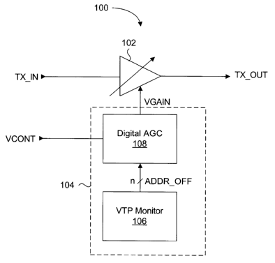
A voltage gain circuit for a transmitter of a wireless core according to an
embodiment
of the present invention is shown in Figure 5. The circuit embodiment of gain
circuit 100
shown in Figure 5 can be used as gain circuit 22 shown in Figure 1. Gain
circuit 100 includes
a variable amplifier 102, and a VTP compensation circuit 104. Since variable
amplifier 102
can be identical to the variable amplifiers 40 of Figures 3 and 4, its
functionality and
operation will be the same as previously discussed for variable amplifiers 40.
VTP
cornpensation circuit 104 is responsible for sensing at least one parameter of
the device, and
appropriately adjusting the compensated gain voltage control signal VGAIN, in
response to
the input control voltage VCONT and the sensed at least one parameter.
VTP compensation circuit 104 includes two major functional blocks. First is a
VTP
manitor 106 and the second is a digital compensator 108. The VTP monitor
circuit 106
includes standard well-known circuits for sensing any one or more of a supply
voltage
parameter, a temperature parameter, and a process parameter. Of course, any
other
measurable parameter can be sensed with a corresponding dedicated circuit. VTP
monitor
circuit 106 then generates a set of digital signals, ADDR_OFF, that
corresponds to the set of
analog voltages in the digital domain provided by the dedicated sensing
circuits. In the
pmsent example, this set of digital signals represents an offset address of n-
bits, where n
cari be any integer value greater than 0. As will be discussed later, the
number of bits of the
address will be determined in part by the resolution of the system. This
offset address is
provided to digital compensator 108, which also receives input control voltage
VCONT. As
pre-viously discussed, VCONT is an analog input control voltage provided by
the base-band
processor for adjusting the gain of variable amplifier 100.
Digital compensator 108 converts VCONT into a set of digital signals m-bits
wide
called a base address ADDR_BASE, which is combined with the offset address
ADDR OFF
prcvided by VTP monitor circuit 106. The combined address is then used to
access a preset
data word, the preset data word effectively representing a digital form of the
compensated
gain control voltage. VGAIN is generated by converting the digital preset word
into an
equivalent analog voltage level. Once again, the resolution of the system can
be optimized
for the application.
Figure 6 is a block diagram showing further details of VTP monitor 106 and
digital
cornpensator 108. Details of VTP monitor 106 will now be discussed. According
to the
present example shown in Figure 6, VTP monitor 106 includes parameter sensing
circuits
120, 122 124, an analog-to-digital (A/D) converter 126, and registers 128.
More specifically,
the parameter sensing circuits can include a temperature sensing circuit 120,
a supply
-8-
CA 02602597 2007-09-27
WO 2006/102741 PCT/CA2006/000460
voltage sensing circuit 122, and a process sensing circuit 124. According to a
preferred
erribodiment of VTP monitor 106, an analog multiplexor 130 is included for
selectively
coupling the sensed voltage from one of the three parameter sensing circuits
to A/D
converter 126. The analog multiplexor 130 is not necessarily required if each
parameter
sensing circuit has its own dedicated A/D converter 126, however, in the
interest of
conserving silicon area, inclusion of the analog multiplexor 130 is preferred.
In the presently
described embodiment, the A/D converters preferably have a 4-bit resolution.
Those of skill
in i:he art will understand that higher or lower resolution converters can be
used according to
the! specific application.
In general operation, the three parameter sensing circuits 120, 122 and 124
provide
analog voltages VTEMP, VSUP, and VPROC respectively, to MUX 130. In response
to a pair
of selection signals (not shown), MUX 130 will selectively and sequentially
pass each analog
voltage to A/D converter 126. If for example A/D converter 126 is a 4-bit
converter, then the
oul:put of A/D converter 126 will generate a 4-bit set of digital signals
(1=4). The registers 128
then latch this first set of digital signals, in accordance with the states of
the pair of selection
signals. In the presently described embodiment, circuit 128 would include at
least 12
individual registers, for latching each 4-bit set of digital signals. Although
not shown in Figure
6, registers 128 includes a multiplexor for selectively passing each 4-bit set
of digital signals
to a corresponding set of registers associated with one digitized parameter.
All the registers
cari be output enabled, to drive all the ADDR_OFF bits simultaneously after
all the
parameters have been sensed and latched. The selection signals (2-bit signal
for 1 of 3
selection) for the de-multiplexor can be the same as those for MUX 130, as
both circuits
would operate synchronously.
Generally, MUX 130 and A/D converter 126 operate as a conversion circuit for
gerierating portions of the offset address ADDR_OFF, which are eventually
combined
together to form the offset address ADDR_OFF. Once all three parameters have
been
serised and provided in digital signal form to registers 128, 12 bit offset
address ADDR OFF
(n=3 sets of signals x4 signals/set=12) is provided to digital compensator
108.
In the interest of conserving silicon area, it is preferable to limit the
number of
ADDR_OFF bus lines, especially in applications employing a higher resolution
A/D converter
126. Therefore, according to another embodiment of VTP monitor 106 and digital
cornpensator 108, registers 128 can include a number of registers equal to the
resolution of
A/D converter 126, and controlled such that each 4-bit set of address bits are
driven serially.
In the present application, with a 4-bit A/D converter 126, registers 128
would include 4
latching circuits, which drive a 4-bit ADDR_OFF signal. Since a full 12 bit
offset address is
required at decoder 142, decoder 142 would include a full set of registers and
a
-9-
CA 02602597 2007-09-27
WO 2006/102741 PCT/CA2006/000460
corresponding multiplexor for passing each 4-bit ADDR OFF signal to a
corresponding set of
registers. Once the entire offset address has been latched in decoder 142,
digital
compensator 108 is ready to receive VCONT. Alternately, registers 128 can be
replaced
with line drivers since decoder 142 would already include a full set of latch
circuits.
Details of digital compensator 108 will now be discussed. Digital compensator
108
includes an A/D converter 140, a decoder 142, and a digital-to-analog (D/A)
converter 146.
The system can include memory 144, directly coupled to the decoder 142 for
receiving
me!mory access signals and for providing addressed memory contents in response
to the
me:mory access signals. Those familiar with semiconductor memory devices will
understand
thait memory access signals can include block decoding signals, wordline
access and column
access signals. Of course, a practical implementation would have decoder 142
and memory
144 integrated together as a single unit. It is noted at this time that memory
144 is pre-loaded
with data words, where each data word can be p-bits in width, and is a digital
representation
of a compensated gain voltage control signal for a specific VCONT voltage
level and specific
voltage levels of the sensed parameters. These data words can be determined
through
calibration and/or modeling, and written to memory during wireless device
manufacture/assembly, or upon activation of the wireless device. In a
practical
implementation, memory 144 includes decoder 142, since the size and
configuration of
memory 144 is directly related to the number of received address bits.
Accordingly, tighter
VGiAIN control can be obtained with a higher resolution system, which
necessitates a larger
memory 144 and a correspondingly larger number of address bits and higher
resolution A/D
and D/A converters.
In a preferred embodiment, memory 144 is a non-volatile memory such as Flash
memory, one time programmable (OTP) memory or ROM for example, so that the
memory
coritents are retained in the absence of power.
Alternately, other well known volatile memories, such as SRAM and DRAM can be
used for storing the data words. In the event of power loss however, the
system would
include an appropriate circuit sub-system to enable writing of the volatile
memory with the
dala words. The data words can be transmitted to the wireless device after
power has been
restored as part of a power up reset sequence, or the wireless device can be
synchronized
with a computer to restore the data words from installed files.
A/D converter 140 receives analog input control voltage VCONT, and converts it
to a
set of digital signals, representing base address ADDR_BASE. Accordingly,
depending upon
the resolution of A/D converter 140, ADDR BASE can be m-bits wide. For
example, A/D
coriverter 140 can be a 4-bit converter. Decoder 142 receives and combines
both
ADDR BASE and ADDR OFF, to generate a decoded address, also known as memory
-10-
CA 02602597 2007-09-27
WO 2006/102741 PCT/CA2006/000460
access signals. Address decoding circuits for memory arrays are well known in
the art.
Those of skill in the art should understand that decoder 142 is configured to
decode the bits
of,ADDR_BASE and ADDR OFF such that one memory location of memory 144 is
accessed. Accordingly, the mapping of the bits of ADDR_BASE and ADDR_OFF to
the
inputs of decoder 142 is preset.
Once memory 144 has received the memory access signals, the contents of a
specific memory location, being a p-bit wide data word, are output to D/A
converter 146
through decoder 142. D/A converter 146, preferably being a p-bit converter,
will convert the
p-bit input into analog voltage VGAIN.
Therefore, an appropriate VGAIN voltage level can be generated in response to
any
VCONT, and compensated for abnormal temperature, supply voltage or process
variations,
to rnaintain a linear relationship between the gain of the variable amplifier
102 and VCONT.
Mareover, since each parameter sensing circuit is dedicated to sensing only
one parameter,
the parameters can be concurrently and independently sensed.
Figures 7-9 show circuit examples of parameter sensing circuits that can be
used in
VTP monitor 106 of Figure 6.
Figure 7 is a circuit of temperature sensing circuit 120, which includes a
temperature
independent current source 200 connected in series between a voltage supply
VDD, bipolar
transistor 202, and VSS. The base terminal of bipolar transistor is connected
to its collector
terrninal and current source 200, while its emitter terminal is connected to
VSS. Since bipolar
transistor 202 inherently has a voltage-temperature dependence, the voltage
level of VTEMP
will vary at about 2mV/degree C.
Figure 8 is a circuit for process sensing circuit 124, which includes a
temperature,
pracess and supply voltage independent current source 204 connected in series
between a
voltage supply VDD, n-channel transistor 206, and VSS. Transistor 206 is diode-
connected,
and its source is connected to VSS. To measure process variations, this
circuit senses the
threshold voltage of transistor 206, which has minimally sized W/L dimensions.
Since
threshold voltage is set during the chip manufacturing process, it only needs
to be sensed
once, during a power up reset sequence for example.
Figure 9 is a circuit of supply voltage sensing circuit 122, which includes
resistors 208
and 210 connected in series between supply voltage VDD and VSS. The output
VSUP is
taken from the common node of resistors 208 and 210. Resistors 208 and 210 are
preferably the same type of resistor, and have the same value. In the present
embodiment,
resistor 208 has a resistance value of R1 ohms, while resistor 210 has a
resistance value of
R2 ohms. Both resistors 208 and 210 can be formed on a semiconductor chip as
doped
- 11 -
CA 02602597 2007-09-27
WO 2006/102741 PCT/CA2006/000460
polysilicon lines or diffusion regions, and preferably have the same layout
and value so that
ternperature or processing differences can be tracked.
Those of skill in the art will understand that there are many different types
of
dedicated circuits that can be employed for sensing a parameter, and those
shown in Figures
7-9 merely represent examples of such dedicated circuits. The range of
temperature, supply
voltage, and threshold voltage variance compensation can be set to the
extremes where the
wireless device would no longer function, or to predetermined ranges based on
the particular
application. For example, for portable wireless devices, it is unlikely that
the wireless device
would be used in a 100 degree Celsius environment by a user, hence the upper
limit can be
recluced to a more practical level. Therefore, the resolution of the system
can be reduced in
orcler to lower power consumption and/or silicon area consumption by using
smaller circuits.
Figures 10a-10b illustrate a method for generating a compensated gain control
voltage in response to sensed parameters and an input control voltage. It is
assumed that
the wireless device includes gain circuit 100 as previously described, and the
memory 144
has been loaded with preset data words. The method starts at step 300 when the
wireless
device is powered up. Immediately following power up, the threshold voltage,
temperature
and supply voltage parameters are sensed in steps 302, 304 and 306
respectively. Each
sensed parameter voltage is converted to a set of digital signals at step 308,
and
subsequently latched in step 310.
At step 312, if all the parameters have been sensed and stored, all the
digital signals
are driven and provided as the offset address ADDR_OFF at step 314. Otherwise,
the
method continues to check until all the parameters have been sensed and
stored. Step 312
is preferred for the embodiment of the VTP monitor 106 shown in Figure 6,
where a MUX
131) is used to share a single A/D converter 126. Alternatively, step 312 is
not required if VTP
menitor 106 includes dedicated A/D converters 126 for each parameter sensing
circuit. At
step 314, the gain circuit is ready to receive input control voltage VCONT and
provide an
appropriate compensated VGAIN output.
Turning to Figure 10b, analog input control voltage VCONT is received at step
316
and a base address ADDR BASE is generated. As previously discussed, VCONT is
provided by baseband processor 12 in response to a base station request to
adjust gain. The
cornbined base address and offset address is decoded at step 318 to generate a
decoded
adciress, or memory access signals, which are provided to memory 144. The
location
specified by the decoded address in memory 144 is accessed, and a
corresponding preset
data word is provided at step 320. The preset data word is received by D/A
converter 146
and a corresponding analog voltage VGAIN is generated at step 322. VGAIN is
-12-
CA 02602597 2007-09-27
WO 2006/102741 PCT/CA2006/000460
subsequently provided to variable amplifier 102, and a corresponding
adjustment of
transmission gain is made.
Returning to Figure 1 Oa, a delay period is executed at step 324 after the
supply
voltage is sensed at step 306. This delay can be set to any desired length of
time, which
determines the frequency at which the parameters are sensed, which
consequently
determines the frequency at which the offset address ADDR OFF is updated.
After the
delay, a determination is made at step 326 to see if the transmitter core 20
is presently in
use. This determination step is preferred to avoid the potential conflicts
where VCONT is
received while the offset address changes due to a new round of parameter
sensing. If not,
thE:n the method returns to step 304 to begin sensing the temperature and
voltage at steps
304 and 306. Otherwise, the method continues to check the status of
transmitter core 20.
Alternately, the method can loop back to delay step 324. It should be noted
that the method
does not need to loop back to step 302, to re-check the threshold voltage,
from step 306,
since the threshold voltage is set during fabrication of the chip.
Therefore, the presently described embodiment of the invention can linearly
control
the relationship between an input control voltage, such as VCONT, and desired
gain from a
variable amplifier circuit, by compensating for a specific manufacturing
process, and
dynamically variable and fixed parameters. In otherwords, the VTP compensation
circuit will
maintain the linear curve 34 of Figure 2 for temperature, supply voltage, and
process
variations, for a specific manufacturing technology.
The previously described circuit blocks of the embodiments of the present
invention
include well known circuits, such as A/D and D/A converters, and are hence not
shown in
further detail as there are many different circuit implementations that can be
used.
In alternate embodiments, input voltage signal VCONT can be provided to MUX
130,
as a fourth input that can be selectively passed to A/D converter 126. Since
registers 128 will
latch the sensed parameter values, MUX 130 can pass VCONT by default such that
A/D
converter 126 can immediately convert VCONT and pass the base address ADDR
BASE to
decoder 142. Thus, silicon area can be conserved since A/D converter 140 is
not required.
As previously discussed, each parameter sensing circuit can have its own
dedicated
A/D converter for parallel conversion of the sensed voltage levels into
digital signals. In this
alternate embodiment, each A/D converter can have a different resolution. For
example, the
tennperature sensing circuit 120 can be coupled to a 4-bit A/D converter for
finer control of
VCiAIN in response to temperature, while supply voltage sensing circuit 122
and process
sensing circuit 124 can be coupled to 2-bit A/D converters if coarser control
is sufficient.
While the presently described embodiments of the invention utilize a memory,
those
of skill in the art will understand that the memory can be any type of non-
volatile memory,
-13-
CA 02602597 2007-09-27
WO 2006/102741 PCT/CA2006/000460
such as EPROM, Flash, ROM, OTP for example. While volatile memories such as
DRAM
and SRAM can be used, those of skill in the art will understand that
additional logic and data
write circuits for interfacing with the baseband processor may be required to
enable writing of
da-ta to the memory in the event of data loss due to battery power failure.
Although the parameters are measured by transistor circuit elements, other
pairameters can be sensed and measured from micro-electro-mechanical devices
(MEMs)
fabricated on a semiconductor chip with equal efficacy. Accordingly, the
presently described
erribodiments of the invention can be applied to applications other than gain
control for
wireless devices. The present invention can be used in any application where
customized
control over an analog voltage is required in view of dynamically changing
parameters.
The above-described embodiments of the present invention are intended to be
examples only. Alterations, modifications and variations may be effected to
the particular
errbodiments by those of skill in the art without departing from the scope of
the invention,
which is defined solely by the claims appended hereto.
-14-