Note: Descriptions are shown in the official language in which they were submitted.
CA 02603768 2007-10-03
WO 2006/110637
PCT/US2006/013278
- 1 -
JOINED SUPERCONDUCTIVE ARTICLES
TECHNICAL FIELD
The present invention is generally directed to superconductive articles and
methods for forming
same. The invention is particularly related to superconductive articles in the
form of joined coated
conductors, and devices incorporating same.
BACKGROUND ART
Superconductor materials have long been known and understood by the technical
community.
Low-temperature (low-TO superconductors exhibiting superconductive properties
at temperatures
requiring use of liquid helium (4.2 K), have been known since about 1911.
However, it was not until
somewhat recently that oxide-based high-temperature (high-TO superconductors
have been discovered.
Around 1986, a first high-temperature superconductor (HTS), having
superconductive properties at a
temperature above that of liquid nitrogen (77 K) was discovered, namely
YBa2Cu307, (YBCO),
followed by development of additional materials over the past 15 years
including Bi2Sr2Ca2Cu3010+y
(BSCCO), and others. The development of high-Tc superconductors has created
the potential of
economically feasible development of superconductor components incorporating
such materials, due
partly to the cost of operating such superconductors with liquid nitrogen
rather than the comparatively
more expensive cryogenic infrastructure based on liquid helium.
Of the myriad of potential applications, the industry has sought to develop
use of such materials
in the power industry, including applications for power generation,
transmission, distribution, and
storage. In this regard, it is estimated that the native resistance of copper-
based commercial power
components is responsible for billions of dollars per year in losses of
electricity, and accordingly, the
power industry stands to gain based upon utilization of high-temperature
superconductors in power
components such as transmission and distribution power cables, generators,
transformers, and fault
current interrupters. In addition, other benefits of high-temperature
superconductors in the power
industry include a factor of 3-10 increase of power-handling capacity,
significant reduction in the size
(i.e., footprint) of electric power equipment, reduced environmental impact,
greater safety, and
increased capacity over conventional technology. While such potential benefits
of high-temperature
superconductors remain quite compelling, numerous technical challenges
continue to exist in the
production and commercialization of high-temperature superconductors on a
large scale.
Among the challenges associated with the commercialization of high-temperature
superconductors, many exist around the fabrication of a superconducting tape
that can be utilized for
formation of various power components. A first generation of superconducting
tape includes use of the
above-mentioned BSCCO high-temperature superconductor. This material is
generally provided in the
form of discrete filaments, which are embedded in a matrix of noble metal,
typically silver. Although
CA 02603768 2007-10-26
- 2
such conductors may be made in extended lengths needed for implementation into
the power industry
(such as on the order of kilometers), due to materials and manufacturing
costs, such tapes do not
represent a commercially fatale product
Accordingly, a great deal of interest has been generated in the so-called
second-generation HTS
tapes that have superior commercial viability. These tapes typically rely on a
layered structure,
generally including a flexible substrate that provides mechanical support, at
least one buffer layer
overlying the substrate, the buffer layer optionally containing multiple
films, an HTS layer overlying
the buffer film, and an electrical stabilizer layer overlying the
superconductor layer, typically formed of
at least a noble metal. However, to date, numerous engineering and
manufacturing challenges remain
prior to fitil commercialization of such second generation-tapes.
Accordingly, in view of the foregoing, various needs continue to exist in the
art of
superconductors, and in particular, provision of commercially viable
superconducting tapes, methods
for fowling same, and power components utilizing such superconducting tapes.
BRIEF DESCRIPTION OP THE DRAWINGS
FIG. 1 illustrates a general layered structure of a superconductive tape
conductor according to
an embodiment of the present invention.
FIG. 2 illustrates an embodiment illustrating a particular structure of a
joined superconductive .
article,
FIG. 3 illustrates another embodiment of a joined superconductive article,
=
FIG. 4 illustrates a splice according to an embodiment.
FIG. 5 illustrates a basic architecture according to a joined superconductive
article according to
yet another embodiment.
FIGs. 6 and 7 illustrate implementation of a superconducting conductor in a
power cable.
FIG. 8 illustrates schematically a power transformer.
FIG. 9 illustrates the basic structure of a generator.
FIG. 10 illustrates a basic schematic of a power grid.
CA 02603768 2007-10-26
-2a-
DISCLOSURE OF INVENTION
According to a first aspect, a superconductive conductor, particularly a
superconductive article,
includes a first superconductive segment having a nominal thickness tõ1, a
second superconductive
segment having a nominal thickness tõ2, and ajoint region comprising a splice
connecting the first and
second superconductive segments together. The splice overlies portions of both
the first and second
superconductive segments along the joint region, the joint region having a
thickness wherein tit is
not greater than at least one of 1 .81ni and 1.8µ2,
According to another aspect, a superconducting article includes a first
superconductive segment
having a first segment end portion, the first segment end portion having
reduced thickness tth a second
superconductive segment having a second segment end portion, the second
segment end portion having
CA 02603768 2007-10-03
WO 2006/110637
PCT/US2006/013278
- 3 -
reduced thickness to, and a joint region comprising a splice connecting the
first and second
superconductive segments together. The splice overlies the first and second
segment end portions
According to another aspect, a superconducting article includes a first
superconductive segment
having a first segment end portion, the first superconductive segment having a
nominal thickness tni
and the first segment end portion having reduced thickness tri that is less
than tni, a second
superconductive segment having a second segment end portion, the second
superconductive segment
having a nominal thickness tii2 and the second segment end portion having
reduced thickness to that is
less than to., wherein the first and second end portions are bonded together
at a joint region. The joint
region has a thickness tjr that is not greater than at least one of 1.8tn1 and
1.8tn2.
According to another aspect, a superconducting article includes a first
superconductive
conductor having a nominal thickness tni, and a second superconductive
conductor overlying the first
conductor along a joint region, the joint region having a thickness not
greater than 1.8 tni.
According to another aspect, a superconducting article includes a first
superconductive segment
comprising a first substrate, a first superconductive layer overlying the
first substrate, and a stabilizer
layer overlying the first superconductive layer. The article further includes
a second superconductive
segment comprising a second substrate, a second superconductive layer
overlying the second substrate,
and a stabilizer layer overlying the second superconductive layer. A joint
region comprising a splice is
provided to connect the first and second superconductive segments together,
the splice comprising
superconductive layer but free of one of a stabilizer layer and a substrate.
MODES FOR CARRYING OUT THE INVENTION
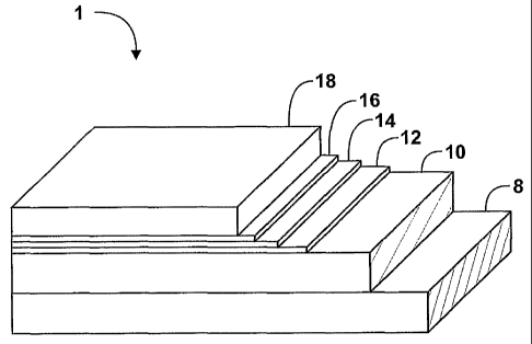
Turning to FIG.1, the generalized layered structure of a superconductive
article according to an
embodiment of the present invention is depicted. The superconductive article
includes a substrate 10, a
buffer layer 12 overlying the substrate 10, a superconductive layer 14,
followed by a capping layer 16,
typically a noble metal layer, and a stabilizer layer 18, typically a non-
noble metal such as copper.
The substrate 10 is generally metal-based, and typically, an alloy of at least
two metallic
elements. Particularly suitable substrate materials include nickel-based metal
alloys such as the known
Inconel group of alloys. The Inconel alloys tend to have desirable creep,
chemical and mechanical
properties, including coefficient of expansion, tensile strength, yield
strength, and elongation. These
metals are generally commercially available in the form of spooled tapes,
particularly suitable for
superconductive tape fabrication, which typically will utilize reel-to-reel
tape handling.
The substrate 10 is typically in a tape-like configuration, having a high
dimension ratio. For
example, the width of the tape is generally on the order of about 0.4 -10 cm,
and the length of the tape
is typically at least about 100m, most typically greater than about 500m.
Indeed, embodiments of the
present invention provide for superconducting tapes that include substrate 10
having a length on the
order of lkm or above. Accordingly, the substrate may have a dimension ratio
which is fairly high, on
CA 02603768 2012-08-08
- 4
the order of not less than 10, not less than about 102, or even not less than
about 103. Certain
embodiments are longer, having a dimension ratio of 104 and higher. As used
herein, the term
'dimension ratio' is used to denote the ratio of the length of the substrate
or tape to the next longest
dimension, the width of the substrate or tape.
In one embodiment, the substrate is treated so as to have desirable surface
properties for
subsequent deposition of the constituent layers of the superconductive tape.
For example, the surface
may be lightly polished to a desired flatness and surface roughness.
Additionally, the substrate may be
treated to be biaxially textured as is understood in the art, such as by the
known RABiTS (roll assisted
biaxially textured substrate) technique, although embodiments herein typically
utilize a non-textured,
polycrystalline substrate, such as commercially available nickel-based tapes
noted above.
Turning to the buffer layer 12, the buffer layer may be a single layer, or
more commonly, be
made up of several films. Most typically, the buffer layer includes a
biaxially textured film, having a
crystalline texture that is generally aligned along crystal axes both in-plane
and out-of-plane of the
film. Such biaxial texturing may be accomplished by IBAD. As is understood in
the art, IBAD is
acronym that stands for ion beam assisted deposition, a technique that may be
advantageously utilized
to form a suitably textured buffer layer for subsequent formation of an
superconductive layer having
desirable crystallographic orientation for superior superconducting
properties. Magnesium oxide is a
typical material of choice for the IBAD film, and may be on the order or 50 to
500 Angstroms, such as
50 to 200 Angstroms. Generally, the IBAD film has a rock-salt like crystal
structure, as defined and
described in US Patent 6,190,752,
The buffer layer may include additional films, such as a barrier film provided
to directly contact
and be placed in between an IBAD film and the substrate. In this regard, the
barrier film may
advantageously be formed of an oxide, such as yttria, and functions to isolate
the substrate from the
IBAD film. A barrier film may also be formed of non-oxides such as silicon
nitride. Suitable
techniques for deposition of a barrier film include chemical vapor deposition
and physical vapor
deposition including sputtering. Typical thicknesses of the barrier film may
be within a range of about
100-200 Angstroms. Still further, the buffer layer may also include an
epitaxially grown film, formed
over the IBAD film. In this context, the epitaxially grown film is effective
to increase the thickness of
the IBAD film, and may desirably be made principally of the same material
utilized for the IBAD layer
such as MgO.
In embodiments utilizing an MgO-based IBAD film and/or epitaxial film, a
lattice mismatch
between the MgO material and the material of the superconductive layer exists.
Accordingly, the
buffer layer may further include another buffer film, this one in particular
implemented to reduce a
mismatch in lattice constants between the superconductive layer and the
underlying IBAD film and/or
epitaxial film. This buffer film may be formed of materials such as YSZ
(yttria-stabilized zirconia)
strontium ruthenate, lanthanum manganate, and generally, perovskite-structured
ceramic materials.
The buffer film may be deposited by various physical vapor deposition
techniques.
CA 02603768 2007-10-03
WO 2006/110637
PCT/US2006/013278
- 5 -
While the foregoing has principally focused on implementation of a biaxially
textured film in
the buffer stack (layer) by a texturing process such as IBAD, alternatively,
the substrate surface itself
may be biaxially textured. In this case, the buffer layer is generally
epitaxially grown on the textured
substrate so as to preserve biaxial texturing in the buffer layer. One process
for forming a biaxially
textured substrate is the process known in the art as RABiTS (roll assisted
biaxially textured
substrates), generally understood in the art.
The superconductive layer 14 is generally in the form of a high-temperature
superconductor
(HTS) layer. HTS materials are typically chosen from any of the high-
temperature superconducting
materials that exhibit superconducting properties above the temperature of
liquid nitrogen, 77K. Such
materials may include, for example, YBa2Cu307.õ, Bi2Sr2Ca2C113010+y,
T12Ba2Ca2Cu3010+y, and HgBa2
Ca2Cu3 Opy. One class of materials includes REBa2Cu307, wherein RE is a rare
earth element. Of
the foregoing, YBa2Cu307,, also generally referred to as YBCO, may be
advantageously utilized. The
superconductive layer 14 may be formed by any one of various techniques,
including thick and thin
film forming techniques. Preferably, a thin film physical vapor deposition
technique such as pulsed
laser deposition (PLD) can be used for a high deposition rates, or a chemical
vapor deposition
technique can be used for lower cost and larger surface area treatment.
Typically, the superconductive
layer has a thickness on the order of about 1 to about 30 microns, most
typically about 2 to about 20
microns, such as about 2 to about 10 microns, in order to get desirable
amperage ratings associated
with the superconductive layer 14.
The capping layer 16 and the stabilizer layer 18 are generally implemented to
provide a low
resistance interface and for electrical stabilization to aid in prevention of
superconductor burnout in
practical use. More particularly, layers 16 and 18 aid in continued flow of
electrical charges along the
superconductor in cases where cooling fails or the critical current density is
exceeded, and the
superconductive layer moves from the superconducting state and becomes
resistive. Typically, a noble
metal is utilized for capping layer 16 to prevent unwanted interaction between
the stabilizer layer(s)
and the superconductive layer 14. Typical noble metals include gold, silver,
platinum, and palladium.
Silver is typically used due to its cost and general accessibility. The
capping layer 16 is typically made
to be thick enough to prevent unwanted diffusion of the components from the
stabilizer layer 18 into
the superconductive layer 14, but is made to be generally thin for cost
reasons (raw material and
processing costs). Typical thicknesses of the capping layer 16 range within
about 0.1 to about 10.0
microns, such as 0.5 to about 5.0 microns. Various techniques may be used for
deposition of the
capping layer 16, including physical vapor deposition, such as DC magnetron
sputtering.
The stabilizer layer 18 is generally incorporated to overlie the
superconductive layer 14, and in
particular, overlie and directly contact the capping layer 16 in the
particular embodiment shown in FIG.
1. The stabilizer layer 18 functions as a protection/shunt layer to enhance
stability against harsh
environmental conditions and superconductivity quench. The layer is generally
dense and thermally
and electrically conductive, and functions to bypass electrical current in
case of failure of the
superconducting layer. It may be formed by any one of various thick and thin
film forming techniques,
CA 02603768 2013-04-03
WO 2006/110637
PCT/US2006/013278
- 6 -
such as by laminating a pre-formed copper strip onto the superconducting tape,
by using an
intermediary bonding material such as a solder or flux. Other techniques have
focused on physical
vapor deposition, typically evaporation or sputtering, as well as wet chemical
processing such as
electro-less plating, and electroplating. In this regard, the capping layer 16
may function as a seed
layer for deposition of copper thereon.
In the particular embodiment shown in FIG. 1, a conductive layer 8 is provided
on the backside
of the substrate 10, that is, the side opposite the constituent layers of the
superconductive article, most
notably the active layer (the superconductive layer 14). The conductive layer
8 may be deposited
simultaneously or during the same processing sequence during formation of the
stabilizer layer 18, and
may be formed of the same material, such as copper. The conductive layer 8 is
typically electrically
conductive (but not superconductive) and may be electrically connected to the
stabilizer layer,
providing additional stabilization functionality.
While the generalized structure of a superconductive article has been
illustrated in connection
with FIG. 1, attention is drawn to FIG. 2. illustrating a more detailed view
of a superconductive article,
particularly, that of a region in which two superconductive segments are
joined together to form a
superconductive article 200, which may have the basic architecture of the
superconductive article 1
illustrated in FIG. 1. Here, similar reference numerals are utilized to denote
analogous structural
features. Description of the constituent layers is not repeated below; the
reader is referred to the
detailed description provided about with respect to the constituent layers of
the superconductive article.
In more detail, superconductive article 200 includes first and second
superconductive
segments la and lb, respectively. Segments 1 a and lb include first and
second
conductive layers 8a and 8b and first and second substrates 10a and 10b, on
which
are disposed a plurality of layers, including first and second buffer layers
12a and 12b, first and second
superconductive layers 14a and 14b, first and second capping layers 16a and
16b, and first and second
stabilizer layers 18a and 18b. As shown, the first and second segments Ia and
lb are positioned so as
to be placed end-to-end. Particularly, the respective ends of the first and
second segments are
positioned to be in general abutting or near-abutting contact at an interface
202. While a slight gap is
shown along the interface 202, the segments may be positioned to be in direct
contact with each other.
According to a particular feature of the embodiment shown in FIG. 2, the first
and second
superconductive segments la and lb are electrically and mechanically joined
together along a joint
region 204. A splice 206 is provided spanning the joint region 204 to provide
electrical and mechanical
connectivity between the segments. In the particular embodiment shown in FIG.
2, splice 206 includes
a layered superconductive structure, generally inverted with respect to the
layered structure of the
segments. Additionally, the splice 206 is free of a stabilizer layer. More
particularly, splice 206
includes a substrate 20, buffer layer 22, superconductive layer 24, capping
layer 26, in the general
sequence as described. The particular splice 206 may be fabricated according
to the basic process flow
for forming the superconductive segments, but foregoing the step of forming a
stabilizer layer.
CA 02603768 2007-10-03
WO 2006/110637
PCT/US2006/013278
- 7 -
Alternatively, a completed superconductive structure may be modified to remove
the stabilizer layer,
and cut into appropriate lengths or coupons to form splice 206.
Splice 206 is bonded to the first and second segments la and lb through use of
a bond layer 25.
Typically, the bond layer 25 is formed of a solder, such as an Indium solder
or a lead-tin solder.
In reference to FIGs. 2 and 5, the first and second segments respectively
include a first segment
end portion 222 and a second segment end portion 224, each of which have a
reduced thickness. More
particularly, the first segment end portion 222 and the second segment end
portion 224 have a reduced
thickness to and to relative to the nominal thicknesses of the first and
second superconductive segments.
Additional description is provided below in connection with FIG. 5.
FIG. 3 illustrates yet another embodiment, somewhat similar to the embodiment
illustrated in
FIG 2. However, generally speaking, the embodiment shown in FIG. 3 utilizes a
different spliced
structure, in which the splice does not incorporate a substrate, but rather,
incorporates a stabilizer layer.
In more detail, superconductive article 300 includes first and second
superconductive segments as
described in connection with FIG. 2. A splice 306 is provided to span joint
region 304. Splice 306
includes a stabilizer layer 38, a capping layer 36a, superconductive layer 34,
and a second capping
layer 36b. Similarly with respect to the embodiment show in FIG. 2, the splice
306 is bonded to the
first and second superconductive segments through use of a bond layer 35.
The particular structure of the splice 306 may be formed in several different
manners. For
example, a completed superconductive segment portion may be delaminated so as
to remove the
substrate from the segment portion, by de-laminating the structure along the
superconductive
layer/buffer layer interface. The delaminated structure including the
stabilizer layer and the
superconductive layer may be optionally then processed so as to deposit a
second capping layer on the
superconductive layer 34.
FIG. 4 illustrates an even further simplified splice 406, which includes a
stabilizer 48 and a
superconductive layer 44. The particular splice structure 306 and 406, shown
in FIGs. 3 and 4
advantageously utilize a stabilizer layer, improving stabilization of the
joint region in practical use.
Accordingly, such splice structures may be preferential for particular
applications in which joint
stabilization is an important parameter.
According to embodiments described herein, the splice generally incorporates a
superconductive layer. This particular aspect helps ensure a desirably low
joint resistance.
Particularly, according to embodiments herein, the superconductive article
incorporating joint
structures such as those described herein have a joint resistance not greater
than about 100 micro-ohms
cm2, such as not greater than about 50 micro-ohms cm2, or even not greater
than 25 micro-ohms cm2.
Additionally, joint resistance may be quantified in terms of heat dissipated,
with an upper limit of not
greater than 0.5 W/cm2 per joint, such as not greater than 0.25 W/cm2 per
joint.
CA 02603768 2013-04-03
WO 2006/110637
PCT/US2006/013278
- 8 -
Turning particularly to FIG. 5, various technical features are illustrated in
connection with
superconductive article 500. Here, superconductive article 500 includes first
and second segments 51a
and Sib, each having a nominal thickness tni and t,a, respectively. These
nominal thicknesses
correspond to the thickness of the respective segments along the majority of
the length of the segments,
particularly excluding the segment end portions, labeled in FIG. 5 as first
segment end portion 522 and
second segment end portion 524. The first and second segment end portions 522
and 524 respectively
have reduced thicknesses, particularly reduced thickness tri and ta, as
illustrated. The reduced
thicknesses associated with the end portions may be achieved through various
architectural changes in
the end portions relative to the main body of the respective segments (having
the comparatively thicker
nominal thicknesses). For example, the ends of the segments may be etched so
as to remove a portion
of the stabilizer layer, and in some embodiments, the entirety of the
stabilizer layer. Alternatively,
during processing, the end portions of the segments may be masked or otherwise
left untreated during
stabilizer deposition. Typically, the reduced thicknesses associated with the
end portions of the
segments are not greater than 90%, such as not greater than 80%, or even 70%
of the nominal
thicknesses of the respective segments. Indeed, in certain embodiments, the
thicknesses of the end
portions may be at a value not greater than 60% of the respective nominal
thicknesses, and in certain
embodiments up to about 50%, half the nominal thickness of the superconductive
segment. Generally,
it is desired that the first and second segments have end portions having
reduced thicknesses within
about 10% of each other, most typically, the reduced thicknesses being equal
to each other, except for
minor variations in thickness due to processing control.
Reduction in the thickness of the superconductive segments along the end
portions thereof enables formation of relatively low-profile joint regions.
In
more detail, referring particularly to the joint 506 in FIG. 5, the joint
region
504 spanning segment end portions 522 and 524 has a thickness tir. Generally,
the
thickness of the joint region lir is not greater than at least one of 1.8 t,
and 1.8 ta. Oftentimes the
profile of the joint region is not greater than about 1.6 tõi or 1.6 ta.
Further, the thickness of the joint
region may be further reduced, such as not greater than at least one of 1.5 to
and 1.5 ta, or not greater
than at least one of 1.3 tni and 1.3 ta. According to one embodiment, the
joint thickness is substantially
equal to the nominal thickness of at least one of the superconductive
segments. While not illustrated in
the drawings, the thickness of the joint region may be below that of one of or
both the thicknesses of
the superconductive segments.
According to embodiments herein, the joined superconductive article may have a
relatively long
length, particularly having a dimension as already described above in
connection with Fig. 1. In
addition, the individual segments may also have relatively extended lengths,
such as having a
dimension ratio not less than about 10, such as not less than about 100, or
even 1000 or higher. The
superconductive article may include additional superconductive segments,
further extending the length
and dimension ratio of the article, each segment being joined according to the
structures and/or
techniques described herein. Extended lengths are particularly suitable for
long distance current
carrying capability, such traversing an urban area or even traversing extended
geographic regions. In
addition, a long length, high dimension ratio superconductive article may be
particularly advantageous
CA 02603768 2007-10-03
WO 2006/110637
PCT/US2006/013278
- 9 -
for deployment in coiled or wound structures such as rotating machines and
transformers, described
below.
According to yet another embodiment, first and second segments having reduced
thickness end
portions may be directly bonded to each other without incorporation of a
splice. In this context, first
and second segments may be joined together in an overlapping fashion such that
the reduced thickness
end portions overlap each other. In this regard, one embodiment contemplates
removal of stabilizer
material along each of the end portions, followed by inversion of one of the
segments and joining.
Alternatively, a joined structure would not require inversion of one of the
segments. Here, a portion of
the stabilizer layer along a first superconductive segment may be removed
while removing a portion of
the conductive layer and/or the substrate along the end portion of the second
superconductive segment,
permitting joining of the two segments without inverting either segment. This
particular structure may
be advantageous for numerous applications, particularly including applications
in which
superconducting segments are deployed in a wound or coiled structure. Although
embodiments
described above rely on a splice for joining in contrast to the forgoing
alternative embodiments, the
alternative embodiments share the concept that superconductive conductors
having reduced thickness
end segments are utilized to execute a low profile joint.
Noteworthy, as used herein, the term 'superconductive conductor' is utilized
to generally denote
a superconductive element, such as either a superconductive segment or a
splice. That is, the term is
used in a generic sense in the present specification and claims.
According to embodiments herein, it should be clear that joined
superconductive articles are
described utilizing a relatively low-profile joint region. This low-profile
joint region may be
particularly advantageous for various industrial applications, particularly
those that would be sensitive
to high profiles or exaggerated profiles along the joint region. Oftentimes,
conventional lap joints have
undesirable excessive profiles, on the order of two times the nominal
thicknesses of each of the
superconductive segments. Such a thickness or profile may not be tolerated in
various applications,
and the mechanical performance of the spliced region according to the state of
the art lap joints may be
compromised.
Turning from particular structures of the superconducting conductors, FIGs. 6
and 7 illustrate
implementation of a superconducting conductor in a commercial power component,
namely a power
cable. FIG. 6 illustrates several power cables 42 extending through an
underground conduit 40, which
may be a plastic or steel conduit. FIG. 6 also illustrates the ground 41 for
clarity. As is shown, several
power cables may be run through the conduit 40.
Turning to FIG. 7, a particular structure of a power cable is illustrated. In
order to provide
cooling to maintain the superconductive power cable in a superconducting
state, liquid nitrogen is fed
through the power cable through LN2 duct 44. One or a plurality of HTS
conductors 46 is/are provided
so as to cover the duct 44. While conventional tapes are generally placed onto
the duct 44 in a helical
manner, the conductors according to embodiments of the present invention need
not be helically
CA 02603768 2013-06-05
=
WO 2006/110637
-
PCT/US2006/013278
-
wound, but, in other embodiments, may extend linearly, parallel to the
longitudinal axis of the power
cable. Further components include a copper shield 48, a dielectric tape 50 for
dielectric separation of
the components, a second HTS tape 52, a copper shield 54 having a plurality of
centering wires 56, a
second, larger LN2 duct 58, thermal insulation 60, provided to aid in
maintaining a cryogenic state, a
5 corrugated steel pipe 62 for structural support, including skid wires 64,
and an outer enclosure 66.
FIG. 8 illustrates schematically a power transformer 70 having a central core
76 around which
a primary winding 72 and a secondary winding 74 are provided. It is noted that
FIG. 8 is schematic in
nature, and the actual geometric configuration of the transformer may vary as
is well understood in the
art. However, the transformer includes at least the basic primary and
secondary windings. In this
10 regard, in the embodiment shown in FIG. 8, the primary winding has a
higher number of coils than the
secondary winding 74, representing a step-down transformer that reduces
voltage of an incoming
power signal. In reverse, provision of a fewer number of coils in the primary
winding relative to the
secondary winding provides a voltage step-up. In this regard, typically step-
up transformers are
utilized in power transmission substations to increase voltage to high
voltages to reduce power losses
over long distances, while step-down transformers are integrated into
distribution substations for later
stage distribution of power to end users. At least one of and preferably both
the primary and secondary
windings comprise superconductive conductors in accordance with the foregoing
description
Turning to FIG. 9, the basic structure of a generator is provided. The
generator includes a rotor
86 that is driven as is known in the art, such as by a turbine. Rotor 86
includes high-intensity
electromagnets, which are formed of rotor coils 87 that form the desired
electromagnetic field for
power generation. The generation of the electromagnetic field generates power
in the stator 88, which
comprises at least one conductive winding 89. According to a particular
feature of the embodiment, the
rotor coils and/or the stator winding comprises a superconductive conductor in
accordance with
embodiments described above. Low loss superconductors used in the stator
windings generally
substantially reduce hysteresis losses.
Turning to FIG. 10, a basic schematic of a power grid is provided.
Fundamentally, the power
grid 110 includes a power plant 90 typically housing a plurality of power
generators. The power plant
90 is electrically connected 92 and typically co-located with a transmission
substation 94. The
transmission substation contains generally a bank of step-up power
transformers, which are utilized to
step-up voltage of the generated power. Typically, power is generated at a
voltage level on the order of
thousands of volts, and the transmission substation functions to step-up
voltages are on the order of
100,000 to 1,000,000 volts in order to reduce line losses. Typical
transmission distances are on the
order of 50 to 1,000 miles, and power is carried along those distances by
power transmission cables 96.
The power transmission cables 96 are routed to a plurality of power
substations 98 (only one shown in
FIG. 10). The power substations contain generally a bank of step-down power
transformers, to reduce
the transmission level voltage from the relatively high values to distribution
voltages, typically less
than about 10,000 volts. A plurality of further power substations may also be
located in a grid-like
fashion, provided in localized areas for localized power distribution to end
users. However, for
CA 02603768 2012-08-08
1
- 11 -
simplicity, only a single power substation is shown, noting that downstream
power substations may be
provided in series. The distribution level power is then transmitted along
power distribution cables 100
to end users 102, which include commercial end users as well as residential
end users. It is also noted
that individual transformers may be locally provided for individual or groups
of end users. According
to a particular feature, at least one of the generators provided in the power
plant 90, the transformers
and the transmission substation, the power transmission cables, the
transformers provided in the power
substation, and the power distribution cables contain superconductive tapes in
accordance with the
present description.
While the invention has been illustrated and described in the context of
specific embodiments, it
is not intended to be limited to the details shown, since various
modifications and substitutions can be
made without departing in any way from the scope of the present invention..
M such, further modifications and equivalents of the invention herein
disclosed may occur to persons
tdcilled in the art using no more than routine experimentation, and all such
modifications and
equivalents are believed to be within the scope of the invention defmed by the
following claims as
purposively construed.