Note: Descriptions are shown in the official language in which they were submitted.
CA 02605827 2007-10-05
THIN FILM TRANSISTOR
BACKGROUND
[0001] The
present disclosure relates to a thin film transistor. In particular, the
thin film transistor comprises a substrate and an oriented zinc oxide
semiconductor
layer.
[0002]
Zinc oxide (ZnO) is known as a channel semiconductor in thin film
transistors ("TFTs"). It
is readily available and can be processed at ambient
temperatures. It also has very high electron mobility (bulk mobility as high
as 155
cm2N=sec and field effect mobility of 70 cm2/V=sec), is environmentally
stable, has a
large band gap, is non-toxic, and inexpensive.
[0003]
However, the method by which the semiconductor is fabricated will affect
the mobility of the ZnO semiconductor layer. A ZnO semiconductor having high
mobility
(5-20 cm2/V=sec) is generally made only through radio-frequency magnetron
sputtering.
Such equipment is expensive and leads to high production costs. In another
approach,
ZnO precursors were used, then processed to form a ZnO semiconductor layer.
However, this approach requires an annealing step at a temperature of 400-550
C.
Such temperatures are not suitable for substrates which deform at lower
temperatures,
like polymeric substrates, such as for example polyester, polycarbonate,
polyimide films
or sheets. ZnO semiconductors have also been made at low (ambient)
temperatures
using ZnO nanoparticles or nanorods in solution. However, such semiconductors
have
low mobility (- 0.6 cm2/V=sec).
[0004]
Zinc oxide thin film crystal usually has a Wurtzite structure (hexagonal
symmetry) with lattice parameters a= 3.2960 and c =5.2065 A. The orientation
of the
zinc oxide can be analyzed using for example x-ray diffraction (XRD)
technique. For
randomly oriented zinc oxide crystals, three peaks can be observed with d-
spacing
distance of d = 2.81, 2.60, 2.48 A for (100), (002), and (101) plane,
respectively, by
using Cu Ka radiation
1.5418 A). The intensity ratios of these peaks in a randomly
oriented zinc oxide powder sample are respectively about I(10o) / 1(002) /
l(1co) = 57 / 44 /
CA 02605827 2007-10-05
100 (intensities are obtained from ICDD/JCPDS card No. 36-1451 provided by The
International Centre for Diffraction Data ). For randomly oriented zinc oxide
crystals,
the percentage of the intensity of the (002) peak relative to the sum of
intensities of
(100), (002), and (101) peak, 1(l00)+1(002)+1(101), 1(002) /
[1(100)+1(002)+1(101)] x 100 %, is about
22 % 2%.
[0005] The following documents provide additional background information:
[0006] E. Fortunato et al., "Fully Transparent ZnO Thin-Film Transistor
Produced
at Room Temperature," Adv. Mater., Vol. 17, No. 5, pp. 590-594 (March 8,
2005).
[0007] T. E. Park et al., "Structural and Optical Properties of ZnO Thin
Films
Grown by RF Magnetron Sputtering on Si Substrates," J. Korean Phys. Soc., Vol.
45,
pp. S697-S700 (December 2004).
[0008] B. J. Norris et al., "Spin coated zinc oxide transparent
transistors," J. Phys.
D: App!. Phys., Vol. 36, pp. L105-L107 (2003).
[0009] B. Sun et al., "Solution-Processed Zinc Oxide Field-Effect
Transistors
Based on Self-Assembly of Colloidal Nanorods," Nano Lett., Vol. 5, No. 12, pp.
2408-
2413 (2005).
[0010] Y. Takahashi et al, "Photoconductivity of Ultrathin Zinc Oxide
Films," Jpn.
J. Appl. Phys., Vol. 33, pp. 6611-6615 (1994).
[0011] D. Bao et al., "Sol-gel derived c-axis oriented ZnO thin films,"
Thin Solid
Films, Vol. 312, pp. 37-39 (1998).
[0012] M. Ohyama et al., "Preparation of ZnO Films with Preferential
Orientation
by Sol-Gel Method," J. Cer. Soc. Jpn., Vol. 104, pp. 296-300 (1996).
[0013] S. Fujihara et al., "Crystallization behavior and origin of c-axis
orientation
in sol-gel-derived ZnO:Li thin films on glass substrates," App!. Sur. Sci.,
Vol. 180, pp.
341-350 (2001).
[0014] K. Nishio et al., "Preparation of highly oriented thin film
exhibiting
transparent conduction by the sol-gel process," J. Mater. Sci., Vol. 31, pp.
3651-3656
(1996).
2
CA 02605827 2010-08-31
[0015] TFTs are generally composed of, on a substrate, an electrically
conductive gate, source and drain electrodes, an electrically insulating gate
dielectric layer which separated the gate electrode from the source and drain
electrodes, and a semiconducting layer which is in contact with the gate
dielectric layer and bridges the source and drain electrodes.
SUMMARY OF THE DISCLOSURE
[0016] The present disclosure relates to, in various embodiments, a
thin film transistor comprising a substrate, a dielectric layer, and a
semiconductor layer, wherein the semiconductor layer comprises zinc oxide
nanodisks oriented with their c-axis perpendicular to the dielectric layer or
the
substrate.
[0017] In further embodiments, the dielectric layer or the substrate has
a surface which includes or has been modified to include at least one type of
polar functional group. The polar functional group further interacts with the
nanodisks, helping them self-assemble into a properly oriented zinc oxide
semiconductor layer.
[0018] In additional embodiments, the substrate may have a
deformation temperature below 300 C. The substrate can be a polymeric
substrate, such as for example polyester, polycarbonate, polyimide films or
sheets.
[0019] In still further embodiments, the semiconductor of the TFT of the
present disclosure has a mobility of at least 1 cm2N.sec. In more specific
embodiments, the TFT has a mobility of at least 5 cm2N.sec.
[0019a] In accordance with another aspect, there is provided a thin film
transistor, comprising:
a substrate;
a gate electrode, a source electrode, and a drain electrode;
3
CA 02605827 2011-12-06
a dielectric layer; and
a semiconductor layer deposited on the substrate or dielectric
layer;
wherein the semiconductor layer comprises zinc oxide
nanodisks; and wherein the surface of the substrate or dielectric layer on
which the semiconductor layer is deposited has at least one type of polar
functional group whereby the zinc oxide nanodisks are preferentially oriented
with their c-axis perpendicular to at least one of the dielectric layer and
the
substrate on which the semiconductor layer is deposited.
[0019b] In accordance with a further aspect, there is provided a thin film
transistor, comprising:
a substrate:
a gate electrode, a source electrode, and a drain electrode;
a dielectric layer; and
a semiconductor layer;
wherein the semiconductor layer comprises zinc oxide
nanodisks oriented with their c-axis perpendicular to the dielectric layer or
the
substrate; and
wherein the semiconductor layer is deposited upon a surface of
the substrate, and the substrate has at least one type of polar functional
group
on the surface.
[0019c] In accordance with another aspect, there is provided a thin film
transistor, comprising:
a substrate;
a gate electrode, a source electrode, and a drain electrode;
a dielectric layer; and
a semiconductor layer;
wherein the semiconductor layer comprises zinc oxide
nanodisks oriented with their c-axis perpendicular to the dielectric layer or
the
substrate; and
3a
CA 02605827 2011-12-06
wherein the semiconductor layer is deposited upon a surface of
the dielectric layer and the dielectric layer has at least one type of polar
functional group on the surface.
[0019d] In accordance with a further aspect, there is provided a thin film
transistor, comprising:
a substrate;
a gate electrode, a source electrode, and a drain electrode;
a dielectric layer; and
a semiconductor layer;
wherein the semiconductor layer comprises zinc oxide
nanodisks oriented with their c-axis perpendicular to the dielectric layer or
the
substrate; and
wherein the substrate is a polymer film or sheet comprising a
polyester, polycarbonate, or polyimide.
[0019e] In accordance with another aspect, there is provided a thin film
transistor, comprising:
a substrate;
a gate electrode, a source electrode, and a drain electrode;
a dielectric layer; and
a semiconductor layer;
wherein the semiconductor layer comprises zinc oxide
nanodisks oriented with their c-axis perpendicular to the dielectric layer or
the
substrate; and
wherein the substrate has a thickness of from about 10
micrometers to about 10 millimeters.
[00191] In accordance with a further aspect, there is provided a thin film
transistor, comprising:
a substrate;
a gate electrode, a source electrode, and a drain electrode;
a dielectric layer; and
a semiconductor layer;
3b
CA 02605827 2011-12-06
wherein the semiconductor layer comprises zinc oxide
nanodisks oriented with their c-axis perpendicular to the dielectric layer or
the
substrate; and
wherein the semiconductor layer further comprises metal
nanoparticles or metal oxide nanoparticles.
[0019g] In accordance with another aspect, there is provided a thin film
transistor, comprising:
a substrate;
a gate electrode, a source electrode, and a drain electrode;
a dielectric layer; and
a semiconductor layer;
wherein the semiconductor layer comprises zinc oxide
nanodisks oriented with their c-axis perpendicular to the dielectric layer or
the
substrate; and
wherein the zinc oxide nanodisks have a height of from about 1
nanometer to about 100 nanometers.
[0019h] In accordance with a further aspect, there is provided a thin film
transistor, comprising:
a substrate;
a gate electrode, a source electrode, and a drain electrode;
a dielectric layer; and
a semiconductor layer, wherein the semiconductor layer
comprises zinc oxide nanodisks oriented with their c-axis perpendicular to the
substrate; and
wherein the zinc oxide nanodisks have a height of from about 1
nanometer to about 100 nanometers.
[0019i] In accordance with another aspect, there is provided a thin film
transistor, comprising:
a polymeric substrate;
a gate electrode, a source electrode, and a drain electrode;
a dielectric layer; and
3c
CA 02605827 2011-12-06
a semiconductor layer, wherein the semiconductor layer
comprises zinc oxide nanodisks oriented with their c-axis perpendicular to the
dielectric layer; and
wherein the zinc oxide nanodisks have a height of from about 1
nanometer to about 100 nanometers.
[0020] Processes for making such TFTs are also disclosed.
[0021] These and other non-limiting characteristics of the disclosure
are more particularly disclosed below.
3d
CA 02605827 2007-10-05
BRIEF DESCRIPTION OF THE DRAWINGS
[0022] The following is a brief description of the drawings, which are
presented
for the purposes of illustrating the exemplary embodiments disclosed herein
and not for
the purposes of limiting the same.
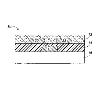
[0023] FIG. 1 is a first exemplary embodiment of a TFT of the present
disclosure.
[0024] FIG. 2 is a second exemplary embodiment of a TFT of the present
disclosure.
[0025] FIG. 3 is a third exemplary embodiment of a TFT of the present
disclosure.
[0026] FIG. 4 is a fourth exemplary embodiment of a TFT of the present
disclosure.
DETAILED DESCRIPTION
[0027] A more complete understanding of the components, processes, and
devices disclosed herein can be obtained by reference to the accompanying
figures.
These figures are merely schematic representations based on convenience and
the
ease of demonstrating the present development and are, therefore, not intended
to
indicate relative size and dimensions of the devices or components thereof
and/or to
define or limit the scope of the exemplary embodiments.
[0028] Although specific terms are used in the following description for
the sake
of clarity, these terms are intended to refer only to the particular structure
of the
embodiments selected for illustration in the drawings and are not intended to
define or
limit the scope of the disclosure. In the drawings and the following
description below, it
is to be understood that like numeric designations refer to components of like
function.
4
CA 02605827 2007-10-05
[0029] In FIG. 1, there is schematically illustrated an TFT configuration
10
comprised of a substrate 16, in contact therewith a metal contact 18 (gate
electrode)
and a layer of a gate dielectric layer 14 on top of which two metal contacts,
source
electrode 20 and drain electrode 22, are deposited. Over and between the metal
contacts 20 and 22 is a zinc oxide semiconductor layer 12 as illustrated
herein.
[0030] FIG. 2 schematically illustrates another TFT configuration 30
comprised of
a substrate 36, a gate electrode 38, a source electrode 40 and a drain
electrode 42, a
gate dielectric layer 34, and a zinc oxide semiconductor layer 32.
[0031] FIG. 3 schematically illustrates a further TFT configuration 50
comprised
of substrate (not shown)/indium-tin oxide (ITO)/an aluminum-titanium oxide
(ATO),
wherein the ITO 56 is a gate, electrode, and ATO 54 is a dielectric layer, and
a zinc
oxide semiconductor layer 52, on top of which are deposited a source electrode
60 and
a drain electrode 62.
[0032] FIG. 4 schematically illustrates an additional TFT configuration 70
comprised of substrate 76, a gate electrode 78, a source electrode 80, a drain
electrode
82, a zinc oxide semiconductor layer 72, and a gate dielectric layer 74.
[0033] The TFT of the present disclosure has a semiconductor layer
comprising
zinc oxide nanodisks oriented with their c-axis perpendicular to the plane of
the
dielectric layer or the substrate. The crystalline zinc oxide in the
semiconductor layer is
preferentially oriented with the c-axis perpendicular to the plane of the
substrate. In
embodiments, this preferential orientation refers to the crystalline zinc
oxide in the
semiconductor layer having a percentage of x-ray diffraction intensity of the
(002) peak
relative to the sum of intensities of (100), (002), and (101) peak, 1(002)1
[1(100)+1(002)+1(101)]
X 100 %, larger than about 40 %, larger than about 60%, larger than about 80%
(or from
about 40% to about 100%, from about 60% to about 100%, from about 80% to about
100%). Electron transport has been found to be most favorable when the
nanodisks are
oriented in this manner.
CA 02605827 2007-10-05
[0034] The term "nanodisk" herein refers to a nanometer-sized object which
has
a 3-dimensional architecture with a height along the c-axis and a base along
the (002)
plane; the base can be a circular (or close to circular), polygonal, or
irregular shape; the
height of the disk is equal to or less than the diameter of the base. Zinc
oxide
nanoplates are also included herein as nanodisks. Each zinc oxide nanodisk may
be a
zinc oxide single crystal or may contain many zinc oxide crystals
(polycrystalline); in the
latter case, zinc oxide crystals in a nanodisk should have a preferential
orientation with
their c-axis perpendicular to the base of the nanodisk. Nanodisks and nanorods
can be
distinguished by their structure; in nanorods, the height of the nanorod is
larger than the
diameter of the base.
[0035] The dielectric layer or the substrate upon which the semiconductor
layer is
deposited may contain or be surface-modified to contain surface polar
functional
groups, such as ¨OH, -NH2, -COOH, -S03H, -P(=0)(OH)2, etc. It has been found
that
the (002) plane of the ZnO nanodisk, which is the most polar and has the
highest
surface energy, will strongly interact with the surface polar functional
groups such that
the nanodisks are preferentially oriented with their c-axis perpendicular to
the dielectric
layer or the substrate.
[0036] The semiconductor of the TFT of the present disclosure has a
mobility of
at least 1 cm2N=sec. This exceeds the mobility of most TFTs fabricated using
other
liquid deposition techniques.
[0037] The zinc oxide semiconductor layer of the present disclosure is
made
using a liquid deposition technique. The technique comprises depositing a
composition
comprising zinc oxide nanodisks over a dielectric layer, a substrate or other
component
of a TFT, optionally heating at a temperature below the deformation
temperature of the
substrate, and optionally cooling. These steps may also be repeated to form a
thicker
semiconductor layer made up of several smaller sublayers.
[0038] A complexing agent is optionally used in the zinc oxide nanodisk
composition, which has the possible benefits of increasing the solubility or
dispersing
capability of zinc oxide nanodisks in a liquid, increasing the viscosity of
the zinc oxide
nanodisk composition to improve thin film uniformity, and facilitating the
formation of
6
CA 02605827 2007-10-05
preferentially oriented zinc oxide nanodisks in the films with the c-axis
perpendicular to
the resulting semiconductor layer. The complexing agent can be, for example, a
carboxylic acid and an organoamine. In embodiments, the complexing agent is an
organoamine selected for example from the group consisting of ethanolamine,
aminopropanol, diethanolamine, 2-methylaminoethanol, N,N-dimethylaminoethanol,
methoxyethylamine, methoxypropylamine, diaminoethane,
diaminopropane,
diaminobutane, diaminocyclohexane, and the like, and mixtures thereof.
[0039] Any
suitable liquid(s) including, for instance, organic solvents and water
can be used to disperse or dissolve zinc oxide nanodisks to form a zinc oxide
nanodisk
composition. Suitable organic solvents include hydrocarbon solvents such as
pentane,
hexane, cyclohexane, heptane, octane, nonane, decane, undecane, dodecane,
tridecane, tetradecane, toluene, xylene, mesitylene, and the like; alcohols
such as
methanol, ethanol, propanol, butanol, pentanol, hexyl alcohol, heptyl alcohol,
ethyleneglycol, methoxyethanol, ethoxyethanol, methoxypropanol,
ethoxypropanol,
methoxybutanol, dimethoxyglycol, and the like, ketones such as acetone,
butanone,
pentanone, cyclohexanone, and the like, tetrahydrofuran, chlorobenzene,
dichlorobenzene, trichlorobenzene, nitrobenzene, cyanobenzene, acetonitrile,
N,N-
dimethylformamide, and mixtures thereof.
[0040] The
concentration of the zinc oxide nanodisk composition is for example
from about 1 % to about 80 % by weight, from about 2% to about 50 % by weight,
and
particularly from about 5 A to about 30 %, by weight of the total zinc oxide
nanodisk
composition. The molar ratio of the optional complexing agent to zinc oxide
nanodisks
is for instance from about 0.1 to about 10, from about 0.2 to about 5, and
particularly
from about 0.5 to about 2.
[0041] In
embodiments, other components can be incorporated in the
composition comprising zinc oxide nanodisks. Such components include, for
example,
a polymer such as polystyrene, poly(methylmethacrylate,
poly(vinylpyrollidone), and the
like, metal nanoparticles of such as gold, silver, and the like, metal oxide
nanoparticles
of such as silicon oxide, gallium oxide, zirconium oxide, aluminum oxide, tin
oxide,
indium-tin oxide (ITO), and the like, and a mixture thereof.
7
CA 02605827 2007-10-05
[0042] Liquid depositing the zinc oxide nanodisk composition can be
accomplished by any liquid deposition techniques such as for instance spin
coating,
blade coating, rod coating, dip coating, screen printing, microcontact
printing, ink jet
printing, stamping and the like.
[0043] In embodiments, the heating step, which is optionally used, refers
to a
heat treaiment at a temperature or several temperatures within a range of
between
about 50 C and about 300 C. The heating can be accomplished for example in
an
instant heating manner at a certain temperature using a pre-heated heating
equipment.
In embodiments, the heating can be accomplished in a gradual heating manner
with a
heating rate that the heating equipment can achieve, ranging from for example
from
about 0.5 to about 100 C per minute starting from room temperature (about 25
C) or
starting from a temperature between about 25 C to about 100 C. In further
embodiments, the heating can also be accomplished step-wise at several
temperatures,
such as, for example, at about 100 C, then at about 200 C, and then at about
300 C.
In embodiments, the heating can also be accomplished step-wise at several
temperatures, combined with gradual heating. The heating can also be
accomplished
for instance at a higher temperature and then at a lower temperature such as
first at
about 300 C and then at about 200 C.
[0044] In embodiments, "cooling", which is optionally used, refers to
bringing the
temperature of the deposited composition to a temperature below about 100 C,
and
particularly to about room temperature (that is, about 25 C). The cooling can
be
accomplished for instance in a self-cooling manner by turning off the heating
equipment
or in a controlled manner at a certain cooling rate such as for example from
about 0.1
C/min to about 100 C/min. In embodiments, a slow cooling such as at a cooling
rate
of about 0.1 C/min to about 10 C/min may be employed especially from a
temperature
higher than about 300 C to reduce mechanical strain in the semiconductor
layer(s) and
the substrate.
[0045] The size of zinc oxide nanodisks used in embodiments can have a
base
diameter of from about 1 nm to about 1000 nm. In specific embodiments, the
base
diameter is from about 1 nm to about 500 nm. In further embodiments, the base
8
CA 02605827 2007-10-05
diameter is from about 2 nm to about 100 nm. The zinc oxide nanodisks can have
a
height of from about 0.5 nm to about 1000 nm in height. In specific
embodiments, the
height is from about 0.5 nm to about 500 nm. In further embodiments, the
height is from
about 1 nm to about 100 nm. Illustrative examples for preparation of zinc
oxide
nanodisks can be found in several articles. M. Monge, M. L. Kahn, A.
Maisonnat, and
B. Chaudret, "Room-Temperature Organometallic Synthesis of Soluble and
Crystalline
ZnO Nanoparticles of Controlled Size and Shape", Angew. Chem. vol.115, 5479
¨5482
(2003), described a method by using dicyclohexyl zinc and organoamines in
tetrahydofuran at room temperature to synthesize zinc oxide nanodisks with
diameters
of 3 ¨ 5 nm. Y. Peng, A. Xu, B. Deng, M. Antonietti, and H. Coolfen, "Polymer-
Controlled Crystallization of Zinc Oxide Hexagonal Nanorings and Disks", J.
Phys.
Chem. B vol. 110, 2988-2993 (2006), disclosed a method for preparation of zinc
oxide
nanodisks of 400 nm to 1000 nm in diameter by heating an aqueous Zn(NO3)2
solution
which contains carboxyl-modified polyacrylamide.
[0046] The zinc oxide semiconductor layer of the present disclosure can
be used
in electronic devices such as large area displays, radio-frequency
identification (RFID)
tags, etc. which use thin film transistors with high field-effect mobility of
for example
greater than 1 cm2N.s.
[0047] The zinc oxide semiconductor layer has a thickness ranging for
example
from about 10 nanometers to about 1 micrometer, particularly a thickness of
from about
20 to about 200 nanometers. The TFT devices contain a semiconductor channel
with a
width, W and length, L. The semiconductor channel width may be, for example,
from
about 0.1 micrometers to about 5 millimeters, with a specific channel width
being about
micrometers to about 1 millimeter. The semiconductor channel length may be,
for
example, from about 0.1 micrometer to about 1 millimeter with a more specific
channel
length being from about 5 micrometers to about 100 micrometers.
[0048] The substrate may be composed of any suitable materials for
instance
silicon, glass, aluminum, or plastics. The thickness of the substrate may be
from about
micrometers to over 10 millimeters with a representative thickness being from
about
1 to about 10 millimeters for a rigid substrate such as glass plate or silicon
wafer.
9
CA 02605827 2007-10-05
[0049] The gate electrode can be a thin metal film, a conducting polymer
film, a
conducting film made from conducting ink or paste or the substrate itself, for
example
heavily doped silicon. Examples of gate electrode materials include but are
not
restricted to aluminum, nickel, gold, silver, copper, zinc, indium, zinc-
gallium oxide,
indium tin oxide, indium-antimony oxide, conducting polymers such as
polystyrene
sulfonate-doped poly(3,4-ethylenedioxythiophene) (PSS-PEDOT), conducting
ink/paste
comprised of carbon black/graphite or colloidal silver dispersion in polymer
binders,
such as ELECTRODAGTm available from Acheson Colloids Company. The gate
electrode can be prepared by vacuum evaporation, sputtering of metals or
conductive
metal oxides, coating from conducting polymer solutions or conducting inks by
spin
coating, casting or printing. The thickness of the gate electrode ranges for
example
from about 10 to about 200 nanometers for metal films and in the range of
about 1 to
about 10 micrometers for polymer conductors. Typical materials suitable for
use as
source and drain electrodes include those of the gate electrode materials such
as
aluminum, zinc, indium, conductive metal oxides such as zinc-gallium oxide,
indium tin
oxide, indium-antimony oxide, conducting polymers and conducting inks. Typical
thicknesses of source and drain electrodes are about, for example, from about
40
nanometers to about 1 micrometer with the more specific thickness being about
100 to
about 400 nanometers.
[0050] The gate dielectric layer generally can be an inorganic material
film or an
organic polymer film. Illustrative examples of inorganic materials suitable as
the gate
dielectric layer include aluminum-titanium oxide, aluminum oxide, silicon
oxide, silicon
nitride, barium titanate, barium zirconium titanate and the like; illustrative
examples of
organic polymers for the gate dielectric layer include polyesters,
polycarbonates,
poly(vinyl phenol), polyimides, polystyrene, poly(methacrylate)s,
poly(acrylate)s, epoxy
resin and the like. The thickness of the gate dielectric layer is, for example
from about
nanometers to about 2000 nanometers depending on the dielectric constant of
the
dielectric material used. An representative thickness of the gate dielectric
layer is from
about 100 nanometers to about 500 nanometers. The gate dielectric layer may
have a
conductivity that is for example less than about 10-12 S/CM.
CA 02605827 2007-10-05
[0051] In
embodiments, the gate dielectric layer, the gate electrode, the
semiconductor layer, the source electrode, and the drain electrode are formed
in any
sequence with the gate electrode and the semiconductor layer both contacting
the gate
dielectric layer, and the source electrode and the drain electrode both
contacting the
semiconductor layer. The
phrase "in any sequence" includes sequential and
simultaneous formation. For example, the source electrode and the drain
electrode can
be formed simultaneously or sequentially.
[0052] For
a n-channel TFT, the source electrode is grounded and a bias voltage
of generally, for example, about 0 volt to about 80 volts is applied to the
drain electrode
to collect the charge carriers transported across the semiconductor channel
when a
voltage of generally about -20 volts to about +80 volts is applied to the gate
electrode.
[0053] In
embodiments, the zinc oxide semiconductor layer in a TFT device
generally exhibits a field-effect mobility of greater than for example about 1
cm2Ns
(square centimeter per Volt per second), and an on/off ratio of greater than
for example
about 103. On/off ratio refers to the ratio of the source-drain current when
the transistor
is on to the source-drain current when the transistor is off.
[0054] It
will be appreciated that various of the above-disclosed and other
features and functions, or alternatives thereof, may be desirably combined
into many
other different systems or applications. Various presently unforeseen or
unanticipated
alternatives, modifications, variations or improvements therein may be
subsequently
made by those skilled in the art which are also intended to be encompassed by
the
following claims. Unless specifically recited in a claim, steps or components
of claims
should not be implied or imported from the specification or any other claims
as to any
particular order, number, position, size, shape, angle, color, or material.
[0055]
While particular embodiments have been described, alternatives,
modifications, variations, improvements, and substantial equivalents that are
or may be
presently unforeseen may arise to applicants or others skilled in the art.
Accordingly,
the appended claims as filed and as they may be amended are intended to
embrace all
such alternatives, modifications variations, improvements, and substantial
equivalents.
11