Note: Descriptions are shown in the official language in which they were submitted.
CA 02605871 2007-10-23
WO 2005/112103 PCTIUS2005/015786
-1-
MICROFABRICATED MINIATURE GRIDS
RELATED APPLICATION(S)
This application claims the benefit of U.S. Provisional Application No.
60/569,132,
filed on May 7, 2004. The entire teachings of the above application(s) are
incorporated herein by reference.
BACKGROUND OF THE INVENTION
The present invention relates generally to a method for manufacturing a grid
for
gating a stream of charged particles. The dimensions of the grid elements
determine
the spatial extent of fields perpendicular to the plane of the grid, such that
finer mesh
grids have improved optical properties.
Certain types of particle measurement instruments, such as ion mobility
spectrometers, make use of a gating device for turning on and off a flowing
stream
of ions or other charged particles. This is accomplished by disposing a
conducting
grid within the path of the ions. Alternately energizing or de-energizing the
grid
then respectively deflects the ions or allows them to flow undeflected.
The most common method for implementing such grid uses an interleaved comb of
wires, also referred to as a Bradbury-Nielson Gate. Such a gate consists of
two
electrically isolated sets of equally spaced wires that lie in the same plane
and
alternate in potential. When a zero potential is applied to the wires relative
to the
energy of the charged particles, the trajectory of the charged particle beam
is not
deflected by the gate. To deflect the beam, bias potentials of equal.magnitude
and
opposite polarity are applied to the two sets of wires. This deflection
produces two
separate beams, each of whose intensity maximum makes a corresponding angle,
alpha, with respect to the path of the un-deflected beam.
CA 02605871 2007-10-23
WO 2005/112103 PCT/US2005/015786
-2-
One approach to manufacturing a gating grid is disclosed in U.S. Patent
4,150,319
issued to Nowak, et al. In this technique, a ring-shaped frame is fabricated
from a
ceramic or other suitable high temperature material. The two sets of wires are
wound or laced on the frame. Each set of wires is actually a single,
continuous wire
strand that is laced back and forth between two concentric series of through-
holes
that are accurately drilled around the periphery of the frame.
Another technique for manufacturing such a gate is described in U.S. Patent
5,465,480 issued to Karl, et al. In this approach, the gating grid elements
are
produced from a thin metal foil by cutting or etching the foil to produce the
grid
structure. The gird elements are connected to side electrodes in a desired
pattern to
produce the two sets of wires. The foil grid structure is made mechanically
stable by
attaching it to an insulating support member. After the then-rigid grid
structure is
affixed to the insulating support member, the grid elements are selectively
severed
from the side electrodes to form the interdigitated grid.
Yet anotlie'r approach for manufacturing such a grid-is described in the paper
by
Kimmel, J.R., et al., entitled "Novel Method for the Production of Finely
Spaced
Bradbury-Nielson Gates," in Review of Scientific Instruments, Vol. 72, No. 12,
Dec.
2001, pp. 4354-4357. In this method, a guide is first manufactured out of a
polymer
block. The guide has a series of evenly spaced parallel grooves. A hole is
drilled
through the center of the polymer block; this hole eventually carries the ion
beam.
The machined polymer block is mounted on an insulated face of an H-shaped
portion of a single sided, copper clad circuit board, with the grooves running
from
top to bottom of the H. The polymer-to-copper clad contacts are then fixed
using an
epoxy. Two small portions of the single sided copper clad board are fixed on
the
bottom side of the polymer in the region where the block extends over the
center bar
of the H-shaped copper frame.
A hand cranked, rotating screw is then used as a weaving instrument. In
particular,
a gold-plated tungsten wire runs from a spool over a directing screw and is
coupled
to the hand cranked screw by a belt. The loose end of the wire is then fixed
such as
CA 02605871 2007-10-23
WO 2005/112103 PCT/US2005/015786
-3-
by using an epoxy. A weight is hung from the wire between the directing screw
and
the spool in order to provide a constant tension on the wire.
A still further method was described in U.S. Patent Publication No. US-2003-
0048059-Al, as published on March 13, 2003. In that method, the grid is
fabricated
using a substrate formed of a ceramic, such as alumina. The substrate serves
as a
rectangular frame for a grid of uniformly spaced wires stretched across a
center
rectangular hole. On either side of the frame, nearest the hole, a line of
contact pads
are formed. Adjacent the line of contact pads, on the outboard side thereof,
are
formed a pair of bus bars. The contact pads and bus bars provide a way to
connect
the wires into the desired two separate wire sets of alternating potential.
Specifically, a metal film is deposited on the surface of both sides of the
ceramic
through vacuum evaporation of gold, using chrome as an adhesion layer, for
example. The metal film is then patterned on the front side to form the
conducting
elements on either side of the hole. The desired metalization pattern can be
defined
by a photo-resist and chemical-etch process, a lift-off process, or by using a
physical
mask during an evaporation. In a next sequence of steps, individual grid wires
are
attached to the fabricated frame. In this process, a spool of wire is provided
that will
serve as the grid wires, with a tensioner arrangement provided to place
constant
tension on the wire as the wires are attached to the substrate.
CA 02605871 2007-10-23
WO 2005/112103 PCT/US2005/015786
-4-
SUMMARY OF THE INVENTION
The present invention relates to fabrication of such grids using
microfabrication
methods such as silicon micromachining, Lithographic Galvanofronung
Aboformung (LIGA) and/or other suitable techniques. A first type of grid is a
Bradbury-Neilson gate that can be used for gating ion beams. A second type of
grid,
a so-called uni potential grid, can be used for creating regions in space with
an
abrupt change in potential gradient.
I. Bradbury-Neilson Gate
In a first embodiment, the invention is a "chopper" for a particle beam
instrument (Bradbury-Neilson gate) which is micromachined in silicon and a
method
for fabricating same. Instead of metal wires or plates electrically isolated
and
supported by an insulating frame, the present invention is microfaricated in
and on
silicon. The grid elements are made from highly doped silicon to provide
electrical
conductors with the required alternating electrical potentials. The alternate
grid
- elements are connected by bus bars also made from highly doped silicon. Part
of the
bus bars are enlarged and metalized to provide bond pads for connection to
associated electronic circuits. ' These electrical conductors are isolated
from a silicon
frame by,a layer of silicon oxide. The grid elements typically have a non-
circular
cross section rather than the circular cross section of wires used for typical
Bradbury-Neilson grids. The oxide coated, silicon frame provides structural
support at the ends of, and intermediate positions along, the electrical
conductors to
allow the cross sectional width of the conductors to be made substantially
smaller
than can be achieved with metal wires.
This type of cliopper is fabricated from a silicon-on-insulator (SOI) wafer
such as is
typically used in the Micro-Electro-Mechanical Systems (MEMS) and/or
semiconductor industry. The SOI wafer used for the chopper manufacture has
three
layers, including a highly doped device layer on the order of 100 microns
thick, an
insulating silicon dioxide layer on the order of 2 microns thick, and a handle
layer
300 to 400 microns thick.
CA 02605871 2007-10-23
WO 2005/112103 PCT/US2005/015786
-5-
The required electrically conducting grid elements and bus bars are fabricated
in the
device layer using high aspect ratio etching. In one particular preferred
embodiment, deep reactive ion etching (DRIE) of silicon, using the Bosch
process,
is used to fabricate these structures. Grid elements with cross sectional
dimensions
less than 1 micron are possible using this process. Grid elements with length
between supports that are 1000 times their width have been manufactured with
this
process.
The required hole(s) in the supporting frame (lzandle layer) is also created
by DRIE.
The remaining silicon dioxide layer between the grid elements maybe removed by
various well known dry or wet etch methods, e.g. reactive ion etching or HF
acid
etching.
One method for fabricating this type of grid comprises the following steps:
a. Spin coat and pattern photoresist on the device side of a silicon-on-
insu.lator (SOI) wafer
b. Deep Reactive Ion Etch (DRIE) trenches on the device side, stopping at
the silicon dioxide layer
c. Spin coat and pattern photoresist on the handle side of wafer
d. Etch the "handle" side silicon, stopping at the silicon dioxide layer
e. Reactive ion etch to remove the silicon dioxide from beneath and between
grid elements
f. Deposit a metal thin fihn and pattern to create bond pads on the device
side
While one etch method has been described, it should be understood that other
processes for micro-fabricating the grid structure are possible. For example,
other
high aspect ratio etch methods, such as crystal orientation dependent silicon
etching
using KOH, plasma-based methods, ion milling, and the like can be used. Wet
etch
methods may also be used for etch steps which do not require highly vertical
side
wall profiles.
CA 02605871 2007-10-23
WO 2005/112103 PCT/US2005/015786
-6-
Ion beam choppers fabricated by this method are an improvement over existing
choppers and fabricating methods. This is true for at least the following
reasons:
1. Grid elements with smaller cross sections and spacing are possible. This
reduces the spatial extent of the fields, which is essential in reducing the
pulse width of the ion packets.
2. The cross sectional aspect ratio can be arbitrarily chosen to have a width
(perpendicular to flight path) to height (parallel to flight path) ratio
greater
than one to achieve high mass range in TOF-MS, equal to unity (an
approximation to a Bradbury-Nielsen gate), or less than one (parallel plate
deflectors) which have greater deflecting power.
3. The manufacturing method(s) described herein use standard, silicon wafer
processing methods which enables the automated production of large
quantities.
II. Uni-potential grids
High resolution time-of-flight mass spectrometers require reflectors (ion
mirrors)
with highly homogeneous electric fields. Each stage of the reflector is
separated by a
mesh or grid to establish a planar potential at the transition between stages.
It is
desirable for the mesh to be largely open to allow a high transmission of the
ion
beam. It is also desirable to have a high density of wires in the mesh in
order to
minimize the distortion of the field in the vicinity of the mesh. This
distortion causes
differences in the flight time of ions which degrades the resolution of the
instrument.
The mesh is also required to be planar in order to minimize differences in
flight
time.
Meshes currently used in ion mirrors are made by etching holes in metal
sheets. The
requirement of high density of wires means the holes must be small. Because
metal
etchants etch laterally as well as perpendicular to the surface at similar
rates, it is
difficult if not impossible to etch a hole smaller than the thickness of the
metal. Thus
small holes forces the metal to be thin. At the same time the requirement of
high
transmission means in a large fraction of the metal must be etched away
resulting in
CA 02605871 2007-10-23
WO 2005/112103 PCT/US2005/015786
-7-
a thin fragile structure which must be mounted under tension in order to
provide a
flat grid.
In the present invention, grids are fabricated from wafers, one example being
silicon
wafers, that can be readily etched by anisotropic methods. Grids with high
transmission can be fabricated with small, closely spaced conducive elements.
The
dimension of the wires perpendicular to the plane of the grid can be greater
than the
in-plane dimension because of the difference in etch rate in the two
directions
resulting in a strong rigid structure. Using the present invention, grid
elements 5
mm long, between support structures, and having a cross section of 5 microns
by
100 microns and spaced 100 microns apart resulting in a transmission of 95%,
are
possible.
More particularly, in a second embodiment, the invention can be used to
fabricate
uni-potential grids that can be used in a number of other types of
instruments. These
grids are fabricated from an ordinary silicon wafer, instead of the SOI wafer
used for
the Bradbury-Neilson gate. However, similar to the above-described process,
the
grid and supporting frame are etched from a single piece of silicon.
The preferred method for making such a grid comprises the following steps.
a. Spin coat and pattern photoresist on side 1 of silicon wafer
b. DRIE trenches on side 1
c. Grow thermal silicon dioxide for KOH mask
d. Spin coat and pattern photoresist on side 2 of wafer
e. Pattern silicon dioxide with HF (hydrofluoric acid) etch
f. Etch exposed silicon in KOH (potassium hydroxide) to thin wafer in area
of the grid elements until grid is suspended over an opening
g. HF etch to remove oxide between grid elements
h. Deposit thin layer of metal onto the grid to produce electrically, highly
conductive surfaces
CA 02605871 2007-10-23
WO 2005/112103 PCT/US2005/015786
-8-
There are several advantages to using this process. Prior art techniques for
manufacturing uni-potential grids used isotropic etching of metals, which
requires
thin metal in order to produce small features. In order for such grids to have
the
required mechanical strength, the solid areas of the grid must be increased in
size.
However, this in turn has the undesirable affect of reducing the ion
transmission of
the grid. High aspect ratio etching which is possible in silicon allows a
higher ion
transmission grid to be produced, by enabling the fabrication of very small
grid
elements with high strength.
In addition, most known processes for etched metal grids often require a means
to
maintain the grid under tension in order to keep the grid flat. Tensioning is
not
required with the more rigid silicon grid of the present invention, in order
to produce
a flat grid.
CA 02605871 2007-10-23
WO 2005/112103 PCT/US2005/015786
-9-
BRIEF DESCRIPTION OF THE DRAWINGS
The foregoing and other objects, features and advantages of the invention will
be
apparent from the following more particular description of preferred
embodiments
of the invention, as illustrated in the accompanying drawings in which like
reference
characters refer to the same parts throughout the different views. The
drawings are
not necessarily to scale, emphasis instead being placed upon illustrating the
principles of the invention.
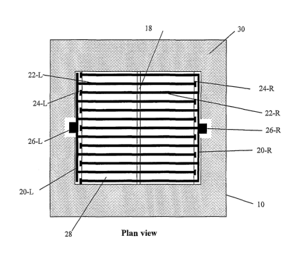
Figs. 1 through 9 pertain to a Bradbury-Neilson type grid. In particular:
Figs. 1 and 2 are a plan view and cross sectional view of the completed grid;
Fig. 3 is a cross sectional view of a Silicon-on-Insulator (SOI) starting
wafer;
Fig. 4 is a section showing the wafer after the photoresist has been applied
and patterned on the device side;
Fig. 5 is a section showing the trenches after the DRIE step on the device
side;
Fig. 6 is a section showing the wafer after it has been mounted on a support
wafer and the photoresist has been applied and patterned on the handle side;
Fig. 7 is a section showing the wafer after the silicon etch step on the
handle
side;
Fig. 8 is a section showing the wafer after the oxide has been etched; and
Fig. 9 is an illustration of a Bradbury-Neilson type grid after the support
wafer is removed.
Figs. 10 through 18 pertain to an etched silicon uni-potential grid that is
manufactured according to the present invention. In particular:
Fig. 10 is a plan view of the completed grid;
Fig. 11 is a section showing the wafer after the photoresist has been applied
and patterned on a first side;
Fig. 12 is a section showing the wafer after the trenches have been etched by
the DRIE step on the first side;
CA 02605871 2007-10-23
WO 2005/112103 PCT/US2005/015786
-10-
Fig. 13 is a section showing the wafer after the growth of thermal oxide on
both sides;
Fig. 14 is a section showing the wafer after it has been mounted on a support
wafer and the photoresist has been applied and patterned on side 2;
Fig. 15 is a section showing the wafer after the oxide has been etched on side
2;
Fig. 16 is a section showing the wafer after the silicon has been etched on
side 2;
Fig. 17 is a section showing the wafer after the oxide has been removed; and
Fig. 18 is a section showing the wafer after a metal coating has been applied
to all surfaces.
Figs. 19 through 24 show process steps for forming the grid using additive
inicromachining techniques, such as LIGA, wherein
Fig. 19 illustrates the starting substrate;
Fig. 20 is a section showing the patterned photoresist;
Fig. 21 is a section showing the deposited conductor material;
Fig. 22 is a section illustrating the result of stripping the photoresist;
Fig. 23 shows removal of a seed layer for metallization; and
Fig. 24 is a section showing the etched hole(s).
Fig. 25 illustrates a single wafer having multiple grids formed thereon.
CA 02605871 2007-10-23
WO 2005/112103 PCT/US2005/015786
-11-
DETAILED DESCRIPTION OF THE INVENTION
A description of preferred embodiments of the invention follows.
The present invention can be used to manufacture an interleaved comb of
conductors
known as a Bradbury-Nielson Gate. Such a gate consists of two electrically
isolated
sets of equally spaced conductors that lie in the same plane and alternate in
applied
voltage potential.
These gates are generally recognized as having a much smaller effective field
size
than the more commonly used deflection plates. They can, for example, be used
to
modulate ion beams in time-of-flight mass spectrometers (TOF-MS), to achieve
mass-to-charge selection. Such gates are also commonly used in ion mobility
mass
spectrometers to regulate the injection of ion packets into a drift tube.
They have also been applied to Hadmard time-of-flight mass spectrometers to
modulate the source ion beam with a pseudorandom sequence of on and off
pulses.
Because the detected signal is then a convolution of the TOF mass spectra, the
signal
can be recovered by again applying the pseudorandom sequence to yield the
single
mass spectrum. The resulting resolution of the instrument depends on the
modulation switching time, which in turn depends on the spatial extent of the
fields
affecting the region surrounding the chopper. Therefore, reduction in the
scale of
the grid elements improves the resolution of the grid.
Figs. 1, 2, and 3 are illustrations of a silicon-on-insulator (SOI) substrate
or portion
of a wafer 10 utilized for providing a substrate for a Bradbury-Nielson type
grid
manufactured according to the present invention. As best seen in the cross
sectional
views of Figs. 2 and 3, the wafer 10 consists of a silicon handle layer 12, a
buried
silicon oxide layer 14, and a highly doped silicon device layer 16. The layers
of the
wafer 10 may have "thickness" dimensions of, for example, 350 um for the
handle
layer 12, 2 um for the oxide layer 14, and 100 um for the device layer 16.
CA 02605871 2007-10-23
WO 2005/112103 PCT/US2005/015786
-12-
The first step (Fig. 4) in a manufacturing process is to deposit and pattern a
top-side
photoresist layer 40 on the device layer 16 of the wafer 10. Numerous
techniques
are known for accomplishing this. In a preferred embodiment, this can be by
spin
coating the photoresist on to the wafer, exposing the photoresist to UV light
through
a mask, and then developing the photoresist to remove desired areas ~of a
pattern that
defines portions of the grid. One such pattern is shown in FIG. 1. The pattern
includes, for example, ground plane area 30, two bus bars 20-L, 20-R, two pads
26-
L, 26-R, two sets of grid conductors 22-L, 22-R, and two sets of grid
conductor
anchors 24-L, 24-R where the end of the conductors are attached to the
insulating
supports 18. The conductors are also supported at intermediate points by
additional
supports 18.
The ground plane areas 30 generally surround the periphery of the wafer 10.
They
serve to electrically define the region surrounding the grid of conductors 22.
The bus bars 20 provide a way to electrically connect each of the two sets of
grid
conductors. Bus bar 20-L, located on the left side of the frame, will be used
to
intercomiect conductors that terminate on the right side of the frame.
Likewise, bus
bar 20-R, located on the right side of the frame, is used to interconnect
conductors
that terminate on the left side of the frame.
The grid conductor anchors 24 provide a place to terminate and support one end
of
the respective conductors. Note that the anchors 24 are defined such that
silicon is
etched around the periphery on three sides thereof. This isolates the anchor
providing an electrically open termination point.
The second step (Fig.5) is to remove the silicon exposed 46 by the removal of
the
photoresist in the first step. This must be done in an anisotropic manner in
order to
form conductors with uniform cross section and spacing. The preferred method
is
deep reactive ion etching (DRIE) using the Bosch process. The silicon oxide
layer
acts as an etch stop.
CA 02605871 2007-10-23
WO 2005/112103 PCT/US2005/015786
-13-
The next step (Fig. 6) is to attach the device side of the wafer 10 to a
support wafer
52. This step may be unnecessary, depending on the equipment used for
manufacture. A handle-side photoresist layer 48 is then deposited and
patterned to
expose the area of the handle layer 12 to be removed. The pattern may include
(Fig.
2) one or more supports 18.
The exposed silicon 50 is then removed using a DRIE process, stopping on the
silicon dioxide layer 14 as shown in Fig. 7. The silicon dioxide lying beneath
and
between the conductors 22 is then removed by reactive ion etching, as shown in
Fig.
8.
The device is then removed from the support wafer 52 (Fig. 9).
A final step typically includes the application of metal to the bond pads 26
to
facilitate electrical connections to the gating grid . This can be achieved by
evaporation or sputtering of a thin film of metal through a shadow mask for
patterning.
In a second embodiment, the invention can be used to fabricate uni-potential
grids.
In the preferred method, the grid is fabricated from an ordinary silicon wafer
instead
of the SOI wafer used for the gating grid, but follows similar steps.
Fig. 10 is an illustration of a uni-potential grid manufactured according to
the
present invention. The grid consists of through holes 64, conducting grid
elements
66, and the surrounding frame 60. Some conducting grid elements may be made
wider to provide structural support throughout the grid structure, without
adversely
affecting the transmission of the grid. In this type of grid, the conductive
elements
run along a second axis which may be perpendicular to a first axis, or have
another
orientation along a preferred crystalographic direction.
The first step (Fig. 11) is to deposit and pattern a photoresist layer 62 on a
first side
of the wafer 58. Numerous techniques are known for accomplishing this. In a
CA 02605871 2007-10-23
WO 2005/112103 PCT/US2005/015786
-14-
preferred embodiment, this can be by spin coating the photoresist on to the
wafer,
exposing the photoresist to UV light through a mask, and then developing the
photoresist to remove desired areas of the pattern. The wafer may have a
thickness
dimension of, for example, 350 um. The grid elements may have a dimension of
10
um or less and the holes may have dimensions on the order of 100 um.
The second step is to remove the silicon exposed 64 by the removal of the
photoresist in the first step. This must be done in an anisotropic manner in
order to
form conductors with uniform cross section and spacing. The preferred method
is
DRIE using the Bosch process. By knowing the etch rate, the etch process can
be
stopped when the desired dimension 65 of the grid elements is reached for
example,
100 um, as shown in Fig. 12.
The next step (Fig. 13) is to grow a thermal oxide layer 68 on surfaces of the
device
to a thickness of, for example, 1 um. The oxide serves as a masking layer for
subsequent wet etching of the silicon.
The next step is to attach the previously etched side of the wafer 58 to a
support
wafer 70 (Fig. 14) A photoresist layer 72 is then deposited and patterned to
expose
the area of the wafer to be removed 74. The exposed silicon oxide is then
removed
to the silicon 58.(Fig. 15) The preferred method is a buffered, HF acid, oxide
etch.
DRIE or a silicon wet etch, such as KOH, is used to remove the silicon 74
(Fig. 16).
The remaining oxide is then removed with a buffered, HF acid, oxide etch or
reactive ion etching with a recipe that is more selective to silicon oxide
than silicon,
producing the grid shown in Fig. 17.
The final step (Fig. 18) is coating the grid with metal to provide a
conducting
surface 76. Numerous techniques are known for accomplishing this. In a
preferred
embodiment, this is accomplished by the vacuum evaporation of gold preceded by
a
chrome adhesion layer.
Yet other microfabrication techniques can be used to manufacture a grid
(either the
Bradbury-Neilson or uni-potential type) according to the invention. The
previously
CA 02605871 2007-10-23
WO 2005/112103 PCT/US2005/015786
- 15-
described preferred embodiments involved removing material from a substrate to
form the conductive grid elements. In this following embodiment, material is
added
to form the conductive grid elements, such as by using a Lithographic
Galvanofomung Aboforming (Lithographic Electroform Molding) or LIGA process.
Fig. 19 is an illustration of a substrate 100 for a grid illustrating the
first step of the
LIGA based process. The substrate 100 may be an insulator or it may be non-
insulating with an insulating layer 102 as shown.
The conductive grid elements are then formed from metal by electroplating. The
insulating layer 102 may be first coated with a thin metal seed layer 104
prior to the
electroplating step. Fig. 20 is an illustration of the second step. A resist
layer 106
is deposited and patterned to fonn a mold 108 for the deposition of the
conductive
grid elements. Numerous techniques, such as photo, x-ray, or e-beam
lithography,
are known for accomplishing this.
The next step is to deposit the conductive grid elements 110 in the mold
pattern as
illustrated in Fig. 21. This may be done by electroplating, if the material is
a metal,
or the conductive grid elements may be formed of other materials such as a
polymer.
Possible metals to use include gold, platinum, tungsten, copper, and nickel.
The resist 106 is then stripped and the seed layer 104, if used, is removed as
illustrated in Fig. 22 and Fig. 23.
Fig. 24 is an illustration of the final step. A hole is formed in the
substrate under the
conductive grid elements 110 by an etching or machining process. Numerous
techniques are known for accomplishing this.
The above description and drawings have shown the resulting conductive
elements
in more or less square cross section. However, it is possible to modify the
cross
sectional shape of the conductors to increase the deflecting power without
increasing
the effective thickness of the grid (which limits the mass range of the TOF-MS
in
CA 02605871 2007-10-23
WO 2005/112103 PCT/US2005/015786
-16-
which the grid is to be placed, for example). The DRIE processes used enable
the
etching aspect ratio of the conductors to be selected to optimize their cross
sectional
shape. For example, a trapezoidal cross section can result, which reduces
scattering
of deflected particles from the sides of the conductive elements, although
this is not
a limitation of the invention.
A number of advantages result from the teachings of the present invention.
Grids that are manufactured using microfabrication techniques according to the
invention can now be batch manufactured such that large numbers of grids are
made
at the same time on the same wafer, as shown in Fig. 25, thereby reducing the
cost
per grid '
Microfabrication techniques typically utilize higlily reproducible, patterning
processes, with submicron resolution, e.g. photo, x-ray or electron beam
lithography.
Microfabricated grids can have conductors with micron-scale and highly
reproducible dimensions, which cannot be achieved by other manufacturing
methods, such as Electrodischarge Machining or Laser ablation. With
microfabrication, feature dimensions are highly reproducible from device to
device,
and from wafer to wafer. Hence, the microfabricated grid is expected to have
better
performance than those manufactured by other means, since performance is
directly
related to conductor size, shape and spacing.
Moreover, by fabricating the conductor elements in single crystal silicon,
instead of
a polycrystalline metal, the conductor elements are mechanically stronger and
more
rigid. Single crystal silicon has a tensile strength and a modulus of
elasticity which
are comparable to steel, but a density that is comparable to aluminum. Hence,
silicon conductors are stiff, strong, and lightweight. These mechanical
attributes,
combined with microfabrication processing, enables them to be self-supporting
at
much greater length-to-width ratios than that which can be achieved with
polycrystalline metal wire or film conductors. With intermediate supporting
structures, the cross sectional dimensions can be reduced to 1 um or less,
while still
fabricating a grid structure large enough to handle a macroscopic particle
beam.
CA 02605871 2007-10-23
WO 2005/112103 PCT/US2005/015786
-17-
Additionally, single crystal silicon micromechanical devices demonstrate no
measurable fatigue. Due to the high strength, low weight and high stiffness of
silicon, silicon conductor elements undergo less displacement during operation
than
metal conductors of similar dimension, minimizing displacement caused
variations
in the field penetration into the surrounding region.
Microfabrication also enables the integrated manufacture of the conductors and
their
supporting substrate, eliminating the labor intensive and error prone assembly
involved in other manufacturing methods, such as manual placement, winding or
stretching of conductive wire elements and bonding of the conductor layer to a
substrate.
While this invention has been particularly shown and described with references
to
preferred embodiments thereof, it will be understood by those skilled in the
art that
various changes in form and details may be made therein without departing from
the
- scope of the invention encompassed by the appended claims.