Note: Descriptions are shown in the official language in which they were submitted.
CA 02606980 2007-10-18
Docket No.: IDR0502CA
METHODS FOR MANUFACTURING RFID TAGS AND STRUCTURES FORMED
THEREFROM
FIELD OF THE INVENTION
100011 The present invention generally relates to the field of radio
frequency
identification (RFID) tags and processes for manufacturing the same.
BACKGROUND OF THE INVENTION
[0002] A RFID tag or electronic barcode is generally used to provide
identification or
other information about a product to which the tag is attached through a
wireless link to a reader
system which captures this information and passes it on, typically in digital
form, to various
database, decision-making, or other electronic tracking systems. This
information is gathered
wirelessly by the RF transmit and receive components of the reader device
which typically
broadcasts a carrier frequency which can provide RF power, clock signal, and
modulation-
encoded commands.
[0003] In the case of passive tags, which are generally most
interesting for low cost tags
as they avoid on-tag power source costs, the carrier frequency signal provides
the RF energy to
power the chip. Clock signal recovery and synchronization are also important
system attributes/
functions which are usually derived from the reader ¨> tag RF signals. The
clock frequency can
define the operating frequency and data communication rates from tag to reader
and from reader
to tag.
[0004] At HF, due to frequency bandwidth concerns imposed by national
and
international regulations, the clock signal is often derived by the tag
circuit by dividing down the
carrier frequency. At UHF frequencies and above, clock signals are typically
derived from
subcarrier frequency modulations on the carrier frequency. This is due to a
number of reasons.
Around 869 MHz and 915 MHz, bandwidth constraints are less restrictive than at
HF frequencies
in Europe and the U.S., respectively. This allows for the addition of
subcarrier modulation of a
- 1 -
CA 02606980 2007-10-18
Docket No.: IDR0502CA
sufficient frequency to allow high speed data communication between reader and
tag. Also,
dividing down the carrier frequency directly requires GHz-speed clocking
circuits and their
associated energy losses. Instead, a 104-105 Hz sub-carrier signal can be
demodulated or
modulated with simple, lower loss subcircuits that can be made with thin film
transistors (TFTs),
diodes, capacitors, inductors and resistors.
[0005] Communication from tag to reader generally occurs through
impedance
modulation. In the HF range and lower, the tag is usually in the near field,
inductive-coupling
range, significantly less than the free space wavelength of the RF carrier. In
this case, there is a
direct inductive coupling between the tag, which typically has a resonant
inductor-capacitor (LC)
loop tuned at or near the carrier frequency, and reader as in the primary and
secondary coils of a
simple inductor-based AC transformer. Modulation of the resonance
characteristics of the LC
loop in the tag, typically through a variable resistive load (which can be
provided by a transistor),
results in a detectable impedance change in the reader front end circuit. The
tag circuitry serially
reads out data via this modulation signal to the reader.
[0006] At UHF frequencies, the reader to tag distance is generally longer,
and the carrier
wavelength is shorter. Due to this, the RF link between the two falls in the
range of
electromagnetic wave propagation physics, as is typically the case in radar,
AM/FM radio or
cellular phone technology. In this case, the tag links to the reader via a
reflected backscatter
signal. By modulating the impedance of the tag's antenna(e), the amount of
power or the phase
or frequency of the signal reflected back to the reader can be changed, and a
time-varying signal
can be encoded with this form of modulation. This modulation can be performed
resistively, as
with a transistor, or through the use of varactors that modulate the imaginary
part of the tag
antennae's impedance.
[0007] On a more basic level, RFID tag circuitry generally performs
some or all of the
following functions:
1. Absorption of RF energy from the reader field.
- 2 -
CA 02606980 2007-10-18
Docket No.: IDR0502CA
2. Conversion of this RF signal into a DC signal that powers the chip.
3. Demodulation of incoming clock, timing and/or command signals available
in the
RF signal from the reader.
4. State machine decision making and control logic that acts on incoming or
preset
instructions.
5. Counter- or register-based reading of data in digital form from a memory
array or
other source (example: output of a sensor).
6. Storage elements (e.g., memory) that store the ID code or other
information that is
to be read out to the reader and/or used for security authentication.
7. Modulation of coded data, timing signals or other commands back to the
tag
antenna(e) for transmission to the tag reader
SUMMARY OF THE INVENTION
[0008] Embodiments of the present invention relate to a radio
frequency identification
(RFID) device and methods for making the same and for making integrated
circuitry for the
same.
[0009] The method generally comprises (a) forming, from a first
silane ink, at least one
first semiconductor layer element on a first surface of a dielectric layer,
the dielectric layer on an
electrically active substrate and the first semiconductor layer element
comprising at least one of a
capacitor plate, a transistor channel region, and a first diode layer; (b)
forming, from a second
silane ink, at least one second semiconductor layer element different from the
first semiconductor
layer element on at least one of the first semiconductor layer element(s) and
the first surface of
the dielectric layer, the second semiconductor layer element comprising at
least one of a second
diode layer, transistor source/drain terminals (when the first silane ink
forms the transistor
- 3 -
I
CA 02606980 2007-10-18
Docket No.: IDR0502CA
channel region), and the transistor channel region (when the first silane ink
does not form the
transistor channel region); and (c) forming at least one metal element on or
over at least one of
the first semiconductor layer element(s) and the second semiconductor layer
element(s), the
metal element comprising at least one of a metal contact, a second capacitor
plate and a metal
gate (when the second silane ink does not form the transistor source/drain
terminals).
[0010] Alternatively, the method may comprise depositing (e.g.,
printing or inkjetting) an
N+ or P+ doped silane ink on the dielectric layer and/or active substrate;
crystallizing the doped
silicon film resulting from the doped silane ink, depositing (e.g., printing
or inkjetting) an N- or
P- doped silane ink in (1) regions for forming transistors and (2) on the N+
or P+ doped silane
ink in regions that will be made into vertical diodes; (optionally) patterning
one or more of the
films formed from the doped silane inks into isolated transistor regions and
mesa regions for
diodes; growing or depositing an oxide film that may function as a capacitor
dielectric (e.g., over
heavily doped regions) and/or a gate dielectric (e.g., over lightly doped
and/or transistor channel
regions); depositing and/or patterning a gate conductor; selectively doping
source and drain
regions; activating the source and drain regions; depositing a dielectric film
in which contact
holes are formed over both transistor and diode regions; (optionally) forming
a contact layer
(e.g., a silicide) in these contact openings; and depositing and patterning a
conductor in direct or
indirect contact with the transistor and diode regions to form interconnect
wiring. The resultant
structure includes capacitors, diodes and transistors on a single substrate,
without necessarily
using a single photolithography mask.
[0011] The RFID device generally comprises (1) a metal antenna and/or
inductor; (2) an
optional interposer strap attached to the antenna or inductor which is at
least partly electrically
conducting; (3) a dielectric layer thereon, configured to support and insulate
integrated circuitry
from the metal antenna and/or inductor; (4) a plurality of diodes and a
plurality of transistors on
the dielectric layer, the diodes having at least one layer in common with the
transistors; and (5) a
plurality of capacitors in electrical communication with the metal antenna
and/or inductor and at
least some of the diodes, the plurality of capacitors having at least one
layer in common with the
- 4 -
1
I
CA 02606980 2007-10-18
Docket No.: IDR0502CA
plurality of diodes and/or at least one metal layer in common with contacts to
the diodes and
transistors.
[0012]
The present invention provides a way to integrate liquid Si deposition
into a cost
effective, integrated manufacturing process for the manufacture of RFID
circuits. Many of the
active semiconductor components, including diodes and transistors, are thin
film-based. Based
on the demonstrated performance of Si ink-derived semiconductor films, in
terms of such
parameters as mobility, doping/carrier concentration, and other parameters,
functional RFID tags
in the LF, HF, UHF, and microwave carrier frequency regimes are possible. The
present thin
film approach utilizing Si ink is attractive as this can be done at relatively
low cost per unit area
which further enables low cost, relatively large die which can be
inexpensively integrated directly
on antennae and/or inexpensively and quickly attached to antennae using
processes such as
conductive adhesive and crimp bonding. Furthermore, the present RFID tags
generally provide
higher performance (e.g., improved electrical characteristics) as compared to
tags containing
organic electronic devices.
[0013] Although the invention is not necessarily limited to any one or any
combination of
the following, novel concepts disclosed herein include:
= Forming some or all of the components necessary for a commercially
acceptable
RFID tag/device by coating and/or selectively depositing silicon (in the
present
case, from a liquid source);
=
Integration of all of the components necessary for a commercially acceptable
RFID tag/device into a relatively low step count process flow;
= Simultaneous growth of oxide on both lightly doped transistor channel
regions
and heavily doped capacitor plate regions to yield both transistor gate oxide
and
capacitor dielectric, respectively;
- 5 -
CA 02606980 2007-10-18
Docket No.: IDR0502CA
= Removal of substrate metal from below some of the active circuit elements
to
limit parasitic capacitance;
= Selection of a stainless steel substrate sealed and/or coated with an
insulator (e.g.,
printed or conventionally deposited spin-on glass [SOG], or a CVD oxide and/or
nitride), allowing the use of both furnace based crystallization as well as
thermal
oxidation of Si for the formation of high mobility and /or high conductivity
silicon
and gate oxide(s), respectively;
= Elongated (lateral) contacts to the lower electrode of the diode, placed
relatively
close to an elongated active region, thereby limiting the series resistance
between
the metallic contacts to the diode, allowing for a simpler and lower cost
overall
integration;
= A heavily doped bottom contact/interconnect layer for diodes, to
eliminate the
need for an additional metal interconnect layer and enable simultaneous growth
of
a capacitor dielectric layer (the diodes can optionally be either p- or n-
/metal
Schottky diodes or p/n diodes);
= Heavily doped silane ink printed or deposited directly on stainless steel
or over a
barrier metal to form the bottom contact of a capacitor;
= Encapsulating and/or protecting the metal substrate (e.g., stainless
steel) with a
spin on glass (SOG) or other insulating layer, including on the backside of
the
substrate, during oxidation or other processing;
= protecting the metal substrate during oxidation or other processing with
silicon
and/or patterned SOG regions, including active and inactive regions of the
frontside and backside of the substrate (and in the case of Si regions, this
allows
for an electrical connection through to the metal substrate as well, which may
be
assisted by n+ or p+ doping);
- 6 -
I
CA 02606980 2007-10-18
Docket No.: IDR0502CA
= Covering the entire top surface of the metal substrate with oxide (except
where it
is covered by Si) to limit contamination by the metal substrate during
subsequent
manufacturing/processing steps, primarily sputter etching;
= Capacitors or capacitor electrodes on an oxide film, either over a foil
substrate
(e.g., stainless steel or aluminum) or in a region without foil, such that
they can be
isolated from the dipoles (antennae) and have relatively low parasitic
capacitance;
= A single metal interconnect layer for many different components of the
circuit
(metal substrate dipole contact, gate conductor contact for interconnect and
capacitors, Si contact for diodes, and contacts to transistor source/drain
terminals),
reducing the total number of metal layers (and therefore the process cost,
although
one should carefully design a layout, integration/manufacturing process and
via/interlayer dielectric [ILD]/metallization process that provide a suitable
circuit
topography and that are compatible with each other; e.g., in the case of a
layout
that includes formation of Schottky contacts, a common metallization such as
Ti/A1 may serve as both interconnect and the Schottky metal where it contacts
undoped or lightly doped semiconductor layers); and
= A self-aligned gate process using a silane ink to get small channel
length, low
capacitance, low foot print, high speed devices for logic and RF operation. A
self-
aligned process may use implantation, solid source doping (e.g., from a SOG),
or
a doped silane as the source and drain doping source, all of which may be self-
aligned across the gate.
100141 These and other advantages of the present invention will
become readily apparent
from the detailed description of preferred embodiments below.
- 7 -
CA 02606980 2007-10-18
Docket No.: IDR0502CA
BRIEF DESCRIPTION OF THE DRAWINGS
[0015] FIG. 1 is a cross-sectional diagram showing structures of an
exemplary device
made by one embodiment of the present manufacturing process.
[0016] FIG. 2 is a cross-sectional diagram showing structures of
another exemplary
device made by another embodiment of the present manufacturing process.
[0017] FIG. 3 shows an exemplary device cross-section and process
flow for making
diode- and capacitor-wired transistors according to the present invention.
[0018] FIG. 4 shows a cross-section of an exemplary diode-wired
transistor manufactured
by the exemplary process flow of FIG. 3.
[0019] FIG. 5 is a layout diagram showing an embodiment of the present
device.
[0020] FIGS. 6A-B are block-level diagrams showing various functional
blocks in
embodiments of the present tags, for both high frequency (HF) and ultra high
frequency (UHF)
applications.
[0021] FIG. 7 is a circuit diagram showing an exemplary 19-stage
oscillator
demonstrating certain commercially acceptable properties for the present
invention.
[0022] FIG. 8 is a graph comparing power conversion efficiencies for
Schottky diodes
manufactured according to the present invention with a commercially available
Schottky diode.
[0023] FIG. 9 is a graph demonstrating rectification up to GHz
frequencies for single
diodes manufactured according to the present invention.
- 8 -
CA 02606980 2007-10-18
Docket No.: IDR0502CA
[0024] FIG. 10 shows results for the exemplary oscillator of FIG. 7
over a range of from
to 20 V.
[0025] FIGS. 11A-11B show results of simulations for the exemplary
oscillator of FIG. 7,
both on-chip (FIG. 11A) and with oscilloscope buffer loading (FIG. 11B).
5 [0026] FIGS. 12A-12B are graphs demonstrating commercially
acceptable switching
speeds, stage delays, and NMOS transistor threshold voltages for the same
devices as for FIG. 9,
but having further undergone a post hydrogenation treatment.
DETAILED DESCRIPTION OF THE PREFERRED EMBODIMENTS
[0027] Reference will now be made in detail to the preferred
embodiments of the
10 invention, examples of which are illustrated in the accompanying
drawings. While the invention
will be described in conjunction with the preferred embodiments, it will be
understood that they
are not intended to limit the invention to these embodiments. On the contrary,
the invention is
intended to cover alternatives, modifications and equivalents, which may be
included within the
spirit and scope of the invention. Furthermore, in the following detailed
description of the
present invention, numerous specific details are set forth in order to provide
a thorough
understanding of the present invention. However, it will be readily apparent
to one skilled in the
art that the present invention may be practiced without these specific
details. In other instances,
well-known methods, procedures, components, and circuits have not been
described in detail so
as not to unnecessarily obscure aspects of the present invention.
[0028] The invention, in its various aspects, will be explained in greater
detail below with
regard to exemplary embodiments.
- 9 -
CA 02606980 2012-02-27
Docket No.: IDR0502CA
An Exemplary Process for Manufacturing RFID Tags
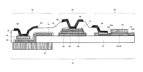
[00291 FIG. 1 shows a first exemplary RFID tag 10, including antenna
20, capacitor 30
coupled thereto, diode 40 and transistor 50. An exemplary process for making
RFID tag 10 shall
be explained below. The exemplary cross-section for tag 10 and a specific
process flow are also
shown on page 37 of U.S. Provisional Patent Application No. 60/697,599
(Attorney Docket No.
IDR0501), filed July 8, 2005, and a version of that process flow adapted to
make a p/n diode (and
corresponding tag cross-section) are shown on page 38 of U.S. Provisional
Patent Application
No. 60/697,599.
100301 First, a spin on glass (SOG) layer 12 may be deposited onto a
conventional metal
foil (e.g., see U.S. Patent Application No. 10/885,283, filed July 6, 2004
(Atty. Docket No
IDR0121), entitled "MOS Electronic Article Surveillance, RF and/or RF
Identification
Tag/Device, and Methods for Making and Using the Same"
). In the present case, an electrically active substrate generally
refers to a substrate having one or more predetermined electrical properties
and/or functions,
such as signal transmission and/or reception (particularly at or in a
predetermined frequency
range), charge storage (e.g., as one or more capacitor electrodes), signal
switching, rectification
and/or filtering, etc. Preferably, the substrate has one or more electrically
conducting and/or
semiconducting properties. Depositing may comprise conventional spin-coating,
printing (e.g.,
inkjet [1.1"] printing), blade coating, dip coating, meniscus coating, slot
coating, gravure
printing, or spray coating a SOG ink composition comprising conventional one
or more SOG
components, one or more conventional solvents for conventional SOG
compositions, and one or
more conventional surfactants, tension reducing agents, binders and/or
thickening agents.
Typically, the SOG layer 12 depositing step is followed by conventional curing
and cleaning
steps.
100311 Next, a heavily doped semiconductor layer 32 is deposited (e.g., by
printing or
inkjetting a silicon-containing ink, such as an n-doped silane; see U.S.
Patent Application Nos.
10/949,013, 10/956,714, 11/246,014 and 11/249,167 [Attorney Docket Nos.
- 10 -
CA 02606980 2012-02-27
Docket No.: IDR0502CA
IDR0302, IDR0303, IDR0422 and IDR0423], respectively filed on
September 24, 2004, October 1, 2004, October 6, 2005, and October 11, 2005
) onto regions of the SOG layer 12
and foil corresponding to capacitor 30 (and at least partly in contact with
subsequently formed
antenna 20) and diode 40. The silicon-containing ink may additionally or
alternatively comprise
one or more semiconductor compounds (e.g., a linear, branched, cyclic or
polycyclic silicon
precursor compound that provides a silicon-containing film upon removal of the
groups
[covalently] bound thereto by conventional processing) and/or one or more
semiconductor
nanoparticles (e.g., of a Group IV element such as Si, Ge, SiGe, etc.).
Alternatively, the ink may
comprise or include one or more semiconductor compounds (such an organic
semiconductor or a
semiconductor precursor compound that provides a semiconductor film [such as
GaAs, CdSe,
CdTe, ZnO, ZnS, etc.] upon removal of ligands and/or covalently-bound groups
by conventional
processing), and/or one or more semiconductor nanoparticles (e.g., of a
semiconductor material
such as GaAs, chalcogenide semiconductors such as ZnO, ZnS, CdSe, CdTe, etc.)
The ink
generally includes a solvent in which the above nanoparticles and/or compounds
are soluble or
suspendable (e.g., a C6-C20 branched or unbranched alkane that may be
substituted with one or
more halogens, a C6-C20 branched or unbranched alkene, a C2-C6 branched or
unbranched allcene
substituted with one or more halogens, a C5-C20 cycloalkane such as
cyclohexane, cyclooctane or
decalin, a C6-C10 aromatic solvent such a toluene, xylene, tetralin, a di-CI-
CI alkyl ether having
a total of at least 4 carbon atoms, and/or a C4-C10 cyclic alkyl ether such as
tetrahydrofuran or
dioxane, etc.; see, e.g., U.S. Patent Application Nos. 10/616,147, filed July
8, 2003 [Attorney
Docket No. KOV-004]
). The
ink may further comprise a surface tension reducing agent, a surfactant, a
binder and/or a
thickening agent, but may advantageously omit such additives or agents.
[0032] Currently, for Schottky diodes, the method comprises forming or
depositing a
heavily doped semiconductor layer first, before formation of other functional
layers in the
Schottky diode. A connection to diode 40 may be formed from capacitor 30, for
example, by
forming, printing or patterning layer 32 such that a strap between the diode
40 and capacitor 30 is
- 11 -
CA 02606980 2012-02-27
Docket No.: IDR0502CA
formed; alternatively, one may make the connection in metal. To the extent
heavily doped layer
32 comprises an amorphous Group IVA element-containing material (e.g., Si
and/or Ge), one
preferably crystallizes the heavily doped layer 32 before subsequently
depositing the next layer.
Thereafter, one or more lightly doped semiconductor layers 44/46 are similarly
deposited or
printed onto the substrate at regions corresponding to diode 40 and transistor
50. Lightly doped
(e.g., N) semiconductor (silicon or [cyclo]silane) ink compositions are also
disclosed in U.S.
Patent Application Nos.
10/949,013, 10/956,714, and 11/249,167. P+ and Fr layers
may be formed by similar printing steps, generally performed immediately
before or immediately
after the N+ and N. regions. The semiconductor regions are then crystallized
(and preferably,
some or substantially all of the dopant therein activated) by furnace
annealing or laser
crystallization, then patterned into active islands. A thin oxide surface
layer 14 is grown thereon
(generally by heating or laser irradiating the structure in an oxidizing
atmosphere, such as
oxygen). This oxidizing step forms both a gate dielectric and a capacitor
dielectric.
Alternatively, the gate dielectric and capacitor dielectric may be formed by
conventional
deposition and patterning of a corresponding dielectric material.
100331
A doped or undoped liquid-phase silicon-containing (e.g., silane) composition
is
then deposited over approximately the middle of transistor region 50 to define
the gate 52 of the
transistor 50 and upper plate 34 of capacitor 30 (see, e.g., U.S. Patent
Application Nos.
10/616,147 [filed on July 8, 2003, as Atty. Docket No. KOV-004], 10/789,317
[filed on February
27, 2004, as Atty. Docket No. IDR0020] 10/949,013 and/or 10/956,714). Thus,
in
one embodiment, depositing the silicon composition comprises printing (e.g.,
inkjetting) a silane
ink. If a doped silane composition is used, multiple layers may be formed. If
an undoped silane
composition is used, a single layer may be formed, and a layer of metal (such
as cobalt [Co] or
nickel [Ni] may be plated (or selectively grown or deposited) thereon
(generally after formation
of dielectric layer 16, e.g., by high-resolution patterning, such conventional
photolithography or
laser lithography/patterning; see paragraph [0034] below). Subsequent heat
treatment (at a
temperature sufficient to crystallize and/or form silicide from the gate
material) generally forms
gate 52 and capacitor plate 34, which in many cases, can be used without
further modification.
- 12 -
CA 02606980 2012-02-27
Docket No.: IDR0502CA
[0034]
However, in one embodiment, a gate metal layer may be photolithographically
defined or laser patterned (preferably by [i] coating a deposited metal layer
with a thermal resist
or other conventional resist containing an IR dye and [ii] selectively
irradiating the resist with a
laser; see, e.g., U.S. Patent Application Nos. 11/084,448 and 11/203,563
[Atty. Docket Nos.
IDR0211 and IDR0213, respectively], filed on March 18, 2005 and August 11,
2005,
respectively
) and excess gate
metal material removed by etching (preferably wet etching). Alternatively, the
gate metal layer
may be defined by other lithographic means including embossing, imprinting or
other high
resolution patterning technology.
100351 After
conventional stripping (e.g., of photoresist, to the extent necessary and/or
desired) and/or cleaning, another SOG layer 16 may be printed or coated onto
the structure. If
printed, one or more of capacitor 30, diode 40 and/or transistor 50
(preferably at least transistor
50) may remain exposed. If coated, portions of SOG layer 16 above capacitor
plate 34, diode
layer 46 and transistor 50 may be removed photolithographically (following
conventional SOG
curing, by coating with a photoresist, irradiating the photoresist through a
mask, etching
[preferably wet etching], then stripping the photoresist and cleaning the
surface of the device) or
by a laser-resist process as described in U.S. Patent Application No.
11/203,563 (Atty. Docket
No. IDR0213, filed on August 11, 2005
). Under appropriate conditions and using known etchant compositions, the
etching
step may also remove the exposed thin oxide film 14, and optionally, a small
amount (e.g., up to
about 30 urn) of lightly doped polysilicon layer 44/46. Any such irradiation
and etching steps
will preferably expose the entire gate layer 52 and remove the SOG layer 16
from over portions
of lightly doped semiconductor layer(s) 44/46 on both sides of gate layer 52
of sufficient
dimensions to form heavily doped source and drain terminal layers thereon and
conductive
contacts thereto. If any part of thin oxide film 14 remains exposed, it is
also removed by etching
(and the resulting surface cleaned) prior to further processing.
- 13-
CA 02606980 2012-02-27
Docket No.: IDR0502CA
[0036]
At this point, a heavily doped semiconductor layer is printed or otherwise
deposited on the exposed surfaces of transistor 50 (e.g., lightly doped
polysilicon layer 44/46 and
gate layer 52), thermally cured, laser irradiated, and the non-crystallized
portions thereof
removed by selective wet etching, to form source and drain contact layers 54a-
b, which may be
self-aligned to gate layer 52 (see, e.g., U.S. Patent Application Nos.
11/084,448 and 11/203,563
[Atty. Docket Nos. IDR0211 and IDR0213, respectively], filed on March 18, 2005
and August
11, 2005, respectively
).
Alternatively, dopant atoms may be introduced into or onto the exposed Si
surfaces via
implantation, plasma deposition, laser decomposition, vapor deposition or
other technique, after
which the doped Si is converted into source and drain contacts by annealing.
As described
above, N+ and P+ regions may be deposited separately (but cured, laser
irradiated and wet etched
in the same processing steps).
[0037]
Contacts (and a first level of metallization) may be formed by metallization
processing conventionally used in the integrated circuit/semiconductor
manufacturing industries
(e.g., sputter a relatively thin barrier and/or adhesive layer 62 such as Ti,
TiN or a TiN-on-Ti
bilayer, then a relatively thick bulk conductor layer 64, such as Al or Al-Cu
alloy (0.5-4 wt.% Cu,
followed by conventional photolithographic definition of contacts and metal
lines that are
subsequently etched [preferably wet etched using a conventional NI-140H/1T202
etch composition
that selectively etches metals such as Al, TiN and Ti relative to a metal
suicide). Alternatively,
similar to gate layer 52, a layer of silicon or barrier metal 62 may be
printed or otherwise
deposited or formed on exposed surfaces of capacitor plate 34, diode layer 46
and transistor 50,
and a conductive metal 64 selectively plated, deposited or printed thereon
(optionally with
subsequent thermal treatment or annealing to form a metal suicide when layer
62 consists
essentially of silicon). Of course, contacts and/or metallization to gate
layer 52 may be formed at
the same time as the contacts and metallization to the capacitor and diode,
generally in an area
outside of the source and drain regions. The photoresist may then be
conventionally stripped,
and the device may be conventionally cleaned. Alternatively, the contacts
and/or metallization
may be patterned by a laser-resist process as described in U.S. Application
No. 11/203,563 (Atty.
- 14 -
CA 02606980 2012-02-27
Docket No.: IDR0502CA
Docket No. IDR0213, filed on August 11, 2005
) or a laser-based process as described in U.S. Patent Application No.
10/722,255 (Atty. Docket No. KOV-015, filed on November 24, 2003
).
[0038] To complete the device, a SOG layer may be printed (e.g., by
inkjetting) or
blanket deposited (e.g., by conventional spin coating, blade coating, screen
printing, dip coating,
meniscus coating, slot coating, gravure printing, or spray coating) over the
device (not shown in
FIG. 1, but shown in FIG. 2 and discussed below). If an additional layer of
metallization is
desired, contact holes over predetermined locations in the metallization layer
62/64 may be
conventionally formed in the SOG layer (or may remain following printing), and
a second layer
of metallization may be formed in the same manner as metallization layer
62/64. An uppermost
cap or passivation layer (e.g., comprising a SOG layer) may then be formed
over the entire device
as described herein, cured, and (optionally) an encapsulant, support or
adhesive may be
laminated thereto.
[0039] The backside of the device (i.e., the metal foil or sheet from which
antenna and/or
inductor 20 is formed) or the interposer is then masked (e.g., with
conventional photoresist, laser
patterned resist, or printed resist/mask material [such as SOG]), etched
(e.g., using a
conventional metal wet etch), and cleaned to form antenna / inductor /
interposer 20. Finally, an
encapsulant (e.g., a conventional water-resistant or water-repellant
encapsulant comprising a
thermoplastic or thermoset resin; not shown in FIG. 1, but shown in FIG. 2 and
discussed below)
may be dispensed onto the etched backside of the device, thereby completing
formation of the RF
ID device 10.
[0040] FIG. 2 shows a cross-sectional view of a substantially
completed, alternative
device 100. Device 100 is, in some respects, a variation (e.g., a "dual
dielectric" embodiment) of
device 10 of FIG. 1. Device 100 includes a barrier dielectric 102 that allows
for capacitors with
low parasitics, as well as non-enclosed contacts for tighter packing density.
-15-
CA 02606980 2012-02-27
Docket No.: IDR0502CA
[00411 Referring now to FIG. 2, a thin, "high k" dielectric material
102 (e.g., Hf0õ) may
be printed or otherwise formed or deposited on dielectric 112 (e.g., from a
sol-gel formulation).
One or more lightly doped polysilicon layers may be formed or deposited (e.g.,
by printing or
inkjetting) thereon similar to polysilicon layers 44 and 46 above, to form
channel layer 144 for
transistors 150a and 150b and (optionally) a base layer 142 for diodes 140a-b
to be subsequently
doped. Alternatively, any of the blanket-deposited or globally deposited
silicon or metal layers
(and optionally, printed silicon or metal layers) may be further defined by
laser patterning ("laser
expos[ing]" where a resist is used). Alternatively, the layers (such as, e.g.,
metal and/or silicon)
may be patterned directly by "laser writ[ing]"; see, e.g., U.S. Patent
Application No. 11/203,563
(Atty. Docket No. IDR0213, filed on August 11, 2005
. These techniques may also be applied to the same layers in the
exemplary process and device depicted in FIG. 1. Thereafter, a gate dielectric
layer (e.g., 114)
may be grown, a gate material printed or otherwise deposited thereon, and
gates 152a and 152b
formed in the same manner as dielectric layer 14 and gate 52 in FIG. 1.
Subsequent etching of
exposed oxide will remove oxide from the source and drain regions of
transistors 150a-b and also
any oxide formed on the polysilicon layer 142 for the diodes.
[00421 Thereafter, a heavily doped lower diode layer 146 and source
and drain terminals
154a-b for transistors 150a and 150b are formed similar to source and drain
terminals 54 or
polysilicon layer 32 above. Thus, lower diode layer 146 and source and drain
terminals 154a-b
may be formed by ion implantation or by printing a heavily doped silane ink as
discussed above.
In one embodiment, lower diode layer 146 comprises an N+-doped silicon layer.
After
crystallization and dopant activation (as described herein and elsewhere), a
second SOG layer
may be printed or otherwise formed thereon, and openings conventionally formed
therein, to
form interlayer dielectric (ILD) 116a-g and 118. A relatively thick, lightly
doped polysilicon
layer may be printed or deposited thereon (particularly in contact openings in
diode regions 140a-
b), similar to polysilicon layer 32 above, to form upper diode layer 148. When
lower diode layer
146 comprises a heavily doped layer, polysilicon layer 148 may be lightly
doped. In this
embodiment, lower diode layer 146 and upper diode layer 148 have different
dopant
- 16 -
CA 02606980 2007-10-18
Docket No.: IDR0502CA
concentrations or densities (e.g., lower diode layer 146 may be N+ doped, and
upper diode layer
148 may be 1\1- doped). In an alternative embodiment, lower diode layer 146
and upper diode
layer 148 have different (or complementary) dopant types (e.g., lower diode
layer 146 may be N+
doped, and upper diode layer 148 may be 13" doped with an optional P+ doped
layer on the
surface). Thereafter, metallization layer 164 may be formed in substantially
the same manner as
metallization 62/64 above to form upper plates for capacitors 120a-b and
contacts to source,
drain and gate terminals of transistors 150a-b and diodes 140a-b.
[0043] An uppermost cap or passivation layer 170 (e.g., comprising a
SOG layer) may
then be formed over the entire device by conventional deposition (e.g., spin-
coating, spray-
coating, inkjet printing, etc.) techniques, then cured. After forming an
antenna, inductor or
resonator (electrically coupled inductor and capacitor) 20, an encapsulant,
support or adhesive
180 may be laminated thereto. Optionally, one may form two, substantially
identical inductors
20a-b. The device 100 is otherwise made as described above for exemplary
device 10 of FIG. 1.
A further variant of this process may use the above mentioned steps, with the
omission of the
vertical diode components, to form RFID circuits using diode-wired transistors
(e.g., formed by
shorting the source to the gate) as the diodes for DC power generation and
signal demodulation.
[0044] FIG. 3 shows a cross-section 182 of an exemplary device 184
connected to
antenna/inductor 186 and a process flow for making diode- and capacitor-wired
transistors. FIG.
4 shows an exemplary diode-wired device 188 with a gate 190 shorted to a
source or drain
terminal 192, and temiinal 192 wired to a source or drain terminal (or lower
diode layer/terminal)
194 of an adjacent device 196. Capacitor-wired transistors can be similarly
formed, with source
and drain terminals wired to each other. In the flow of FIG. 3, a transistor
is wired
conventionally, and a capacitor is made by shorting the source and drain
together as one terminal
and using the gate as the other terminal. Notably, the process flow of FIG. 3
is considerably
shorter and contains fewer steps than the process flows for making the devices
of FIGS. 1-2. In
fact, the process flow of FIG. 3 may contain only one step that involves
printing a silane ink
(although one may use be two silane ink printing steps, one for n-channel
devices and one for p-
- 17 -
CA 02606980 2007-10-18
Docket No.: IDR0502CA
channel devices, for complementary MOS transistors). Such devices (including
the diode- and
capacitor-wired transistors) show performance characteristics suitable for use
in 13.56 MHz
RFID tags. Naturally, the wiring for shorting (i) gate and (ii) source or
drain contacts together
(as well as wiring for shorting source and drain contacts together) is not
shown in the cross
section of FIG. 3, and would be located elsewhere in the transistor layout,
either in front of or
behind the plane of the page. Notably, the flow of FIG. 3 shows that a single
inkjetted silane
layer can be formed (step 4), and this silane layer can be crystallized and
oxidized in the same
processing step in a furnace (step 5). Separate ion implantation steps (steps
10 and 13) are then
used to form NMOS and PMOS transistors/devices.
An Exemplary RFID Device
[0045] In another aspect, the present invention concerns a layout
that includes various
component regions, such as the exemplary devices of FIGS. 1-4. FIG. 5 shows an
exemplary
layout for device 200, including logic region 210, antenna regions 220 and
225, and charge pump
area 230. The device 200 may have a length of from 1 to 25 mm, preferably 5 to
20 mm, a width
of from 1 to 5 mm, preferably 1 to 3 mm, and an overall area of from 1 to 100
mm2, preferably
10 to 50 mm2. In one example, the device is 2 mm x 12.5 mm. As will be
discussed in more
detail with regard to FIGS. 4A-4B, logic region 210 may further comprise an
input/output control
portion, a memory or information storage portion, a clock recovery portion,
and/or an
information/signal modulation portion.
[0046] Antenna region 220 is coupled to charge pump region 230 by L-shaped
bus 222.
A part of charge pump region 230 also overlaps with antenna region 225. Charge
pump region
230 is conventionally coupled to antenna regions 220 and 225 by capacitors,
diodes and/or
interconnects. For example, charge pump region 230 may comprise a plurality of
stages (in one
specific example, 8 stages), and the capacitors therein may have an area of
100 to 400 square
microns per antenna overlap portion (i.e., the portion of charge pump 230 that
overlaps with
either bus 222 or antenna region 225).
-18-
CA 02606980 2007-10-18
Docket No.: IDR0502CA
[0047]
A block diagram of a HF tag design is shown in FIG. 6A and a UHF tag design
is
shown in FIG. 6B. The HF tag design comprises antenna 305, clock recovery
block 310,
demodulator block 320, RF-DC converter block 330, modulator block 340, logic
and 110 control
block 350, and memory 360. The UHF tag design comprises dipole antenna 355,
demodulator/
clock recovery block 370, UHF-DC converter block 380, modulator block 340',
logic and VO
control block 350, and memory 360. Clock recovery block 310, antennae 305 and
355, and
busses from the antennae to demodulator blocks 320 and 370 and to power
converter blocks 330
and 380 operate at or near the carrier frequency, and therefore, require high
speed devices.
[0048]
These circuit blocks can be constructed from thin film device structures,
including
the following devices:
1.
Antennae: at HF, this is most inexpensively fabricated as a planar spiral
inductor
coil with a resonant tank capacitor coupled thereto (e.g., in charge pump
region
230 in FIG. 5). The low resistivity requirements for a high quality (high
voltage!
power extracting) LC coil necessitates the use of metal foils or thick printed
films.
In the UHF, the antenna is typically in a full or half-wave dipole or dipole-
derivative form that supports transmission (and reception) of AC waves without
significant DC conduction or long conduction distances as in a coil. Also, the
skin depth of the excitation in the antennae is shallower in the UHF. For that
reason, UHF antennae can be thin metal foils or even printed conductor films
from materials such as Ag pastes. In certain design embodiments, the HF or UHF
antennae could be formed directly in the underlying metal substrate for the
integrated circuitry, or the substrate could form an interposer or strap
(e.g., a thin
plastic or glass sheet serving as a substrate for subsequent formation of
silicon-
based devices) of intermediate size (e.g., between that of the full antennae
and that
of the semiconductor device-containing integrated circuit area) that could
then be
attached to an external antennae.
-19-
CA 02606980 2007-10-18
Docket No.: IDR0502CA
2. RF-to-DC conversion: This function may be provided by rectifiers
(typically in a
voltage doubler configuration) at any applicable frequency, or from thin film
diode structures formed from a silane-based ink at UHF or HF frequencies. At
HF
frequencies, it is also possible to use diode-connected TFTs (i.e., having its
gate
connected to a source or drain of the same transistor). Such thin film diodes
and
diode-connected TFTs can also be used for voltage clamps and/or voltage clamp
circuits for DC conversion and/or output of DC voltage(s). Modeling of thin
film
devices based on silane ink-based layers with mobilities of > 10 cm2/vs in the
diode transport direction, doping in the range of 1017-1020 cm-3, and contact
resistances on the order of 1 CO ohm-cm2 can support rectification in the GHz
regime, of sufficient efficiency to power a RFID circuit. GHz rectification to
DC
and < 2 nsec gate delays have been demonstrated experimentally for a vertical
thin
film silane ink diode structure and a self-aligned TFT structure,
respectively,
formed as described herein.
3. Demodulator: Demodulation of clock and data signals, encoded as a
subcarrier or
subcarrier modulation on the carrier RF signal, can be achieved with simple
voltage detectors based on thin film diodes or diode-connected TFTs as
described
elsewhere herein. Optimal signal extraction may require filtering and the use
of
tuned capacitors.
4. Logic to perform control and readout (I/0) functions can be realized
with TFTs in
CMOS or NMOS technologies, using materials as described herein. CMOS
technology has a significant advantage in terms of power efficiency, but may
require additional process steps compared to NMOS technology.
5. Memory: simple read-only memory (ROM) can be provided by a digital
resistive
network, defined during the fabrication process. One-time programmable (OTP)
ROM may comprise a conventional fuse or anti-fuse structure, and nonvolatile
- 20 -
I
CA 02606980 2007-10-18
Docket No.: IDR0502CA
EEPROM in thin film form may comprise a TFT having a floating gate therein.
Programming and erasing circuitry (and devices configured to withstand
programming and erasing voltages) can also be designed conventionally and
manufactured as described herein.
6.
Modulator: in the HF range, modulation is typically done by load modulation
with a shunting transistor in parallel with a resonant capacitor (e.g., in the
modulator block or formed from the same layer of material as the antenna; see,
e.g., U.S. Patent Application Nos. 10/885,283 and 11/243,460 [Attorney Docket
Nos. IDR0121 and IDR0272], respectively filed on July 6, 2004 and October 3,
2005). With a modulator TFT manufactured from a silane-based ink in
enhancement mode, when the transistor is on, the LC coil that forms the tag's
antenna can be shorted. This dramatically reduces the Q of the circuit and the
coupling to the reader coil. When the TFT is switched sufficiently 'off,' the
Q of
the LC coil is restored. In this way, a modulation signal can be passed from
the
tag to the reader. In the UHF range, similar effects also vary the scattering
cross-
section of the antenna and modulate the backscatter signal to the reader. This
can
be done with load modulation TFTs changing the impedance of the antenna, and
therefore, the backscatter signal. Due to potential power losses associated
with
this technique, it may be advantageous to use a varactor-based modulation that
shifts the imaginary part of the impedance of the UHF antennae using either a
MOS capacitor device or a varactor diode that can be formed using the TFT and
diode processes described herein for logic TFTs and for rectifier and/or
demodulator diodes.
[0049]
Layouts of thin film transistors configured for logic and memory have been
designed in accordance with the present invention using 8 gm and 2 gm design
rules. Under the
8 gm rules (assuming 2 gm margin for registration/alignment variations), the
average transistor
-21-
I
CA 02606980 2007-10-18
Docket No.: IDR0502CA
area is 9776 m2, and one can place about 100 transistors per mm2. Under the 2
m rules, the
average transistor area is 3264 ,m2, and one can place about 300 transistors
per mm2.
[0050] Typically, RFID tag operation is limited by the minimum RF
field (and power)
required to power the tag. Once the tag is able to power up and sustain the
required voltages,
tag-to-reader communications are possible.
Examples and Results
[0051] Using a process consistent with that described herein for
making diodes, Schottky
diodes having a titanium silicide contact layer were fabricated that are
capable of rectification at
> 1GHz. Prototypes of discrete RF front end circuits were manufactured, and
the operation of
such circuits at 900 MHz were also demonstrated. NMOS transistors having
mobilities > 50
cm2N-sec and as high as 100 cm2N-sec and PMOS transistors having mobilities >
40 cm2N-sec
were manufactured by such a process. CMOS inverters and oscillators were
formed from
interconnected transistors manufactured by such a process. The oscillators
were capable of
operation at 10-25 MHz. Stage delays of 10 ¨ 1.1 ns were obtained between
inverters in series
(e.g., between stages of a ring oscillator). This demonstrates a maximum
switching speed for
logic from this process in excess of 950 MHz. These data, alone and/or in
combination with
other information (e.g., circuit block data and/or simulations) demonstrate
that the present
invention is capable of achieving UHF and HF RFID operation.
[0052] 900MHz SCHOTTKY DIODE PERFORMANCE. Schottky diodes
manufactured
according to the present invention (e.g., from a silicon ink) and having a
titanium silicide contact
layer ("Kovio Si diodes") had a power conversion efficiency > 5% at 900 MHz;
compare line
410 (the present invention) with line 420 (for an HSMS-8250 Schottky diode,
commercially
available from Agilent Technologies) in FIG. 7. Optimized process cleanliness
should further
improve this diode performance, for example by reducing leakage and short
circuits.
- 22 -
CA 02606980 2012-02-27
Docket No.: IDR0502CA
100531 RF FRONT END. As shown by line 510 in FIG. 8, GHz rectification
between 10-
20% for single diodes at 900MHz has been demonstrated for diodes manufactured
according to
the present invention ("Kovio Si diodes"). Thus, diodes manufactured according
to the present
invention comprise working 900 MHz free space devices capable of generating DC
power.
Further optimization in manufacturing integration and circuit design should
further improve the
frequency response and rectification efficiency.
[0054] Using two such diodes in a UHF --0 DC rectifier block (see,
e.g., block 380 in
FIG. 6B), sufficient power was generated from a UHF source providing a 900 MHz
carrier
frequency signal in a prototype RFID tag equipped with a half dipole antenna
to light an LED
electrically coupled to a 100 mW reader (i.e., where the LED and reader
effectively replace the
logic and/or I/O control block 350 in the RFID tag of FIG. 6B).
[0055] Prototypes of functional front-end blocks (e.g., blocks 310-330
and 370-380) for a
RFID tag having Schottky diodes manufactured according to the present
invention have
demonstrated properties shown in the following Table 1:
Process Si Ink + CoSi Top Schottky Si Ink + TiSi Top
Schottky
Ideality Factor 1.75 1.5
I,, Pa] 500 1300
RS (()1 101 19
Rica Ikal 60 5
Table 1. RFID Front End Prototype Properties.
- 23 -
CA 02606980 2012-02-27
Docket No.: IDR0502CA
[0056]
All four properties for the device(s) made using the "Si Ink + TiSi Top
Schottky"
process as shown in Table 1 above are commercially acceptable for item-level
UHF tagging.
[0057]
LOGIC SUMMARY. Data from prototype devices (e.g., MOS transistors) and
circuits for logic and/or I/O control block 350 in FIGS. 4A-B manufactured
using silicon ink as
described herein (but which was used to make only prototype NMOS and PMOS
TFTs) have
shown >> 1 MHz operational capability. This frequency of operation is
sufficient for
commercially acceptable UHF and HF RFID tags. Such silicon ink CMOS IC
devices, when
manufactured using a self aligned silicon ink TFT process flow (see, e.g.,
U.S. Application No.
11/084,448, filed March 18, 2005 [Attorney Docket No. IDR0211]
) have mobilities as high as 100 cm2N-sec, thereby verifying the suitability
of the
manufacturing process herein for commercial production of low-cost RFID tags.
CMOS
inverters manufactured using such a process flow are capable of MHz
oscillation speeds (i.e.,
switching in less than 1 psec). Furthermore, NMOS devices manufactured using
such a process
flow have threshold voltages suitable for commercially acceptable UHF and HF
RFID tags.
[00581 SILICON INK CMOS OSCILLATOR RESULTS. A 19-stage ring oscillator 600
having the design shown in FIG. 7 was fabricated with 6 um CMOS integrated TFT
buffer stages
610a-610t. Stage delays were < 0.1 msec at 10 V operation. FIG. 10 shows
results for this
exemplary oscillator over a range of from 10 to 20 V, including the effects of
probe loading (the
bottom plot 710 showing results for 10 V operation, the middle plot 720
showing results for 15 V
operation, and the upper plot 730 showing results for 20 V operation). Thus,
CMOS transistors
manufactured using the silicon ink technology described in this application
are feasible for UHF
RFID logic (1-5 MHz) and HF RFID Logic (13.56 MHz). Very high speeds are
possible for
small channel devices (< 10 nsec / stage for ¨ 2 pm transistors operating at
10 V).
[00591
FIGS. 11A-11B show results of simulations for the exemplary 19-stage
oscillator,
both on-chip (FIG. 11A) and with oscilloscope buffer loading (FIG. 11B), at 10
V operation.
The simulations used TFT model data extracted from the devices described above
with regard to
- 24 -
CA 02606980 2012-02-27
Docket No.: IDR0502CA
FIG. 8. The values in FIGS. 11A-11B compare the measured data for the logic
(CMOS) devices
above with the simulated data to validate extraction and measurement
capabilities and further
validate the demonstrated results. The oscillator was simulated using CMOS TFT
buffer stages
having transistors with a 6 um effective length (Leff = 6 pm). The oscillation
frequency was 350
kHz, with a stage delay of 70 ns. As one can tell, the shape of the plot 860
in FIG. 11B is quite
similar to the shape of the plots in FIG. 8. The results in FIGS. 12A-12B and
Table 2 below
demonstrate commercially acceptable switching speeds (fswitett > 10 MHz),
stage delays (td <0.1
pee), and NMOS transistor threshold voltages (Vt < 0.5 V), for the same
devices as for FIG. 8,
but having further undergone a post hydrogenation treatment. The two curves of
FIGS. 12A and
12B are respectively for ¨ 6 micron and ¨ 2 micron channel length CMOS TFT
oscillators.
Graph 5A 5B
Leff 6 gm 2 gm
Fos, 3.3 MHz 25 MHz
td 8 nsec 1.1 nsec
Fõx switch 130 MHz 950 MHz
Table 2. Properties for Oscillators of Graphs 12A-12B.
CONCLUSION / SUMMARY
[0060]
The foregoing descriptions of specific embodiments of the present invention
have
been presented for purposes of illustration and description. They are not
intended to be
exhaustive or to limit the invention to the precise forms disClosed, and
obviously many
modifications and variations are possible in light of the above teaching. The
embodiments were
chosen and described in order to best explain the principles of the invention
and its practical
application, to thereby enable others skilled in the art to best utilize the
invention and various
- 25 -
I
CA 02606980 2007-10-18
Docket No.: IDRO5 02CA
embodiments with various modifications as are suited to the particular use
contemplated. It is
intended that the scope of the invention be defined by the Claims appended
hereto and their
equivalents.
- 26-
I