Note: Descriptions are shown in the official language in which they were submitted.
CA 02607554 2010-11-15
ELECTRONIC BALLAST HAVING A FLYBACK CAT-EAR POWER SUPPLY
FIELD OF THE INVENTION
[0001[ The present invention relates to electronic ballasts and, more
particularly, to
electronic dimming ballasts for gas discharge lamps, such as fluorescent
lamps.
BACKGROUND OF THE INVENTION
[00021 Electronic ballasts for fluorescent lamps typically include a "front
end" and a "back
end". The front end typically includes a rectifier for changing alternating-
current (AC) mains line
voltage to a direct-current (DC) bus voltage and a filter circuit for
filtering the DC bus voltage. The
ballast back end typically includes a switching inverter for converting the DC
bus voltage to a high-
frequency AC voltage, and a resonant tank circuit having a relatively high
output impedance for
coupling the high-frequency AC voltage to the lamp electrodes.
[00031 The front end of electronic ballasts also often include a boost
converter, which is an
active circuit for boosting the magnitude of the DC bus voltage above peak of
line voltage, and for
improving the total harmonic distortion (THD) and power factor of the input
current to the ballast.
However, boost converters typically include integrated circuits (IC) and
semiconductor switches,
such as field effect transistors (FETs). In order to handle the amount of
current required to drive the
lamp at high end (i.e. at or near 100% light intensity), the components of
such a boost converter are
typically large and costly.
[0004] A prior art ballast 100 will be described with reference to the block
diagram shown in
Fig. 1 and the voltage and current waveforms shown in Figs. 2a - 2d and is
explained in greater
detail in U.S. Patent No. 6,674,248, issued on January 6, 2004, entitled
"Electronic Ballast".
CA 02607554 2007-11-01
WO 2006/118976 PCT/US2006/016113
-2-
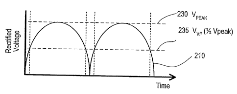
[00051 The ballast 100 includes an electromagnetic interference (EMI) filter
115 and a
rectifier 120 both capable of being connected to an AC power supply such as a
typical 120V, 60 Hz
AC main. The EMI filter 115 isolates high-frequency noise generated by the
ballast circuitry from
the AC power supply. The rectifier 120 converts the AC input voltage to a
rectified pulsating DC
voltage 210, which has a maximum value of UPEAK (shown as 230 in Fig. 2a). For
example, if the
AC input voltage has an RMS (root mean square) value of 277V, the value of
VPEAK will be
approximately 392V. The rectifier 120 is connected to a valley-fill circuit
130 through a diode 140.
A high-frequency filter capacitor 150 is connected across the inputs to the
valley-fill circuit 130.
The valley-fill circuit 130 selectively charges and discharges an energy-
storage device, such as one
or more capacitors, so as to fill the "valleys" between successive rectified
voltage peaks to produce a
substantially DC bus voltage 220. The DC bus voltage is the greater of either
the rectified voltage,
or the voltage across the energy storage device in the valley-fill circuit
130.
[00061 The outputs of the valley-fill circuit 130 are in turn connected to the
inputs to an
inverter 160. The inverter 160 converts the rectified DC voltage to a high-
frequency AC voltage.
The outputs of the inverter 160 are connected to an output circuit 170, which
typically includes a
resonant tank, and may also include a coupling transformer. The output circuit
filters the inverter
160 output to supply essentially sinusoidal voltage, as well as provide
voltage gain and increased
output impedance. The output circuit 170 is capable of being connected to
drive a load 180 such as a
gas discharge lamp; for example, a fluorescent lamp.
[00071 An output current sense circuit 185 coupled to the load 180 provides
load current
feedback to a control circuit 190. The control circuit 190 generates control
signals to control the
operation of the valley-fill circuit 130 and the inverter 160 so as to provide
a desired load current to
the load 180. A power supply 110 is connected across the outputs of the
rectifier 120 to provide the
necessary power for proper operation of the control circuit 190.
[00081 A schematic representation of a prior art valley-fill circuit 330 that
may be used with
ballast 100 is shown in Fig. 3a. The rectified pulsating DC voltage 210 (in
Fig. 2a) is provided to
the valley-fill circuit 330 through diode 140. Two energy-storage capacitors
280, 282 are provided
in the valley-fill circuit 330. These energy-storage capacitors 280, 282
charge in series with a
charging current flowing through capacitor 280, diode 284, capacitor 282, and
a resistor 286, which
limits the magnitude of the charging current. The energy-storage capacitors
280, 282 are sized such
CA 02607554 2007-11-01
WO 2006/118976 PCT/US2006/016113
-3-
that the same voltage, the valley-fill voltage VvF (shown as 235 in Fig. 2a),
is produced across each
capacitor. The magnitude of the valley-fill voltage VvF is approximately one-
half of the peak,
VPEAK, of the rectified pulsating DC voltage 210, which is about 200V when
VPEAK is 392V.
However, the energy-storage capacitors 280, 282 discharge in parallel, with
current flowing through
diode 288 to allow capacitor 280 to discharge, and through diodes 290 and 292
to allow capacitor
282 to discharge. Thus, a.DC bus voltage 220 is formed across the valley-fill
circuit 330 as shown
in Fig. 2b.
[0009) When the rectified voltage 210 is greater than the valley-fill voltage
VvF, i.e. one-half
of the peak of the AC mains line voltage, the inverter 160 draws current
directly from the AC power
supply, through the EMI filter 115 and the rectifier 120, to drive the lamp.
When the rectified
voltage 210 is less than the valley-fill voltage VvF, then the inverter 160
draws current from the
energy-storage capacitors in parallel. This results in the ballast drawing an
input current 240 from
the AC mains only during a relatively large duration of each line half-cycle
centered about the peak
of the line voltage, which allows for unwanted harmonics and undesirable total
harmonic distortion
(THD).
[00101 In order to lower the THD, the input current of the ballast should be
as sinusoidal as
possible (as shown by 250 in Fig. 2c). One approach to making the input
current more sinusoidal is
to implement power supply 110 as a cat-ear power supply, which ideally draws
an input current 260
(shown in Fig. 2d) near the zero crossing of the AC mains input voltage
waveform at either the
leading edge of each half-cycle, or the trailing edge of each half-cycle, or
both. When the current
drawn by the cat-ear power supply is added to the inverter current 240, the
input current waveform is
shaped to be more nearly sinusoidal, such that the input current THD is
substantially reduced, and
the power factor of the ballast is increased. The cat-ear power supply derives
its name from the
shape of its input current waveform that "fills in" the current waveform drawn
by the ballast from
the AC mains around the zero crossings (the shape resembling the ears of a
cat). That is, the input
current waveform typically rises from zero sinusoidally to a value
substantially below peak, then
falls sharply to zero, or rises from zero sharply to a value substantially
below peak, then falls
sinusoidally to zero. The cat-ear power supply typically "steals" power from
the line when the back
end is not drawing current directly from the line. The cat-ear power supply
may be provided with
circuitry that "cuts in" and "cuts out" the power supply in response to fixed
input voltage levels.
CA 02607554 2007-11-01
WO 2006/118976 PCT/US2006/016113
-4-
Along with helping to reduce THD and improve power factor, the cat-ear power
supply also supplies
the power necessary to operate the control circuit 190.
[00111 A prior art cat-ear power supply 310 is shown in Fig. 3b. The cat-ear
power supply
310 is designed with fixed voltage cut-in and cut-out points and will only
draw current from the AC
mains when the rectified voltage 210 is below a predetermined value. This
condition will occur
from a predetermined time before a line voltage zero crossing to a
predetermined time after the line
voltage zero crossing. The cut-out and cut-in voltage points can be adjusted
so that the cat-ear
power supply 310 draws current during a first interval from a time just after
the line voltage zero
crossing to a time when the energy storage capacitor in the valley-fill
circuit 130 begins drawing
charging current from the line, and during a second interval from a time when
the valley-fill energy
storage capacitor stops drawing charging current from the line until the next
line voltage zero
crossing.
[00121 When the rectified voltage 210 is lower than a predetermined voltage, a
charging field
effect transistor (FET) 312 conducts to allow charging of energy-storage
capacitor 314, which
charges toward a voltage Vcc. Alternatively, when the rectified line voltage
is equal to or greater
than the predetermined voltage, then cut-out transistor 318 begins conducting.
The collector of the
cut-out transistor 318 pulls the cathode of a Zener diode 320 toward Vcc,
which effectively turns off
the charging FET 312. The predetenmined cut-in and cut-out voltages are
determined by the
resistive voltage divider network including resistors 322 and 324, to which
the base of the cut-out
transistor 318 is connected.
[00131 The rate of charge of the capacitor 314 is determined by aresistor 316
in series with
the drain of the MOSFET transistor 312. To allow for a substantially piece-
wise continuous ballast
input current, the value of the current drawn by cat-ear power supply 310
should be substantially the
same as the current that will be drawn by the back end of the ballast 100 at
the predetermined cut-out
and cut-in times. In conjunction with the value of the capacitor 314, resistor
316 can be chosen so
that the current drawn will have a desired maximum current that is
substantially the same as the
current that will be drawn by the back end at the predetermined cut-out and
cut-in times and such
that the current drawn will substantially match the shape of the AC mains
voltage.
CA 02607554 2007-11-01
WO 2006/118976 PCT/US2006/016113
-5-
[00141 However, the current drawn from Vcc by the control circuit 190 of
ballast 100 is not
constant throughout the operation of the ballast. Consequently, the current
required to charge
capacitor 314 is sometimes smaller, thus the time required to charge capacitor
314 is shorter.
Therefore, the current drawn by cat-ear supply 310 sometimes does not reach
the desired maximum
current at the predetermined cut-out and cut-in times as shown by 360 in Fig.
3c. When the cat-ear
supply input current 360 is-added to the current 240 drawn by the back end,
the resulting ballast
input current 370 (shown in Fig. 3d) is not completely sinusoidal, thus
contributing to the THD of
the ballast.
[00151 Additionally, in order to obtain the appropriate shape of the input
current waveform,
the power dissipated by the resistor may be very large. For example, the power
into the cat-ear
power supply with the input current 260 (in Fig. 2d) may be approximately four
watts each half-
cycle. If the maximum power consumption of the control circuit 190 is
approximately 0.5 watts,
then 3.5 watts must be dissipated in the resistor 316 during each half-cycle.
This means that the
resistor 316 must be physically large in order to handle the required power
dissipation.
[00161 Thus, there exists a need for a cat-ear power supply for an electronic
ballast that is
more efficient and draws the appropriate amount of current when the back end
is not drawing current
directly from the line in order to reduce the THD of the ballast. Further,
there exists a need for an
electronic dimming ballast that has the reduced THD of a ballast having an
active boost converter,
but does not require the large, expensive components of such boost converters.
SUMMARY OF THE INVENTION
[00171 In accordance with a first feature of the invention, a novel electronic
ballast for
driving a gas discharge lamp includes a rectifier to convert an AC mains input
voltage to a rectified
voltage, a valley-fill circuit to fill the valleys between successive
rectified voltage peaks to produce a
substantially DC bus voltage, a DC-to-AC voltage inverter having series-
connected switching
devices to convert the substantially DC bus voltage to a high-frequency AC
voltage signal for
driving the gas discharge lamp, a resonant tank for coupling the high
frequency AC voltage signal to
the gas discharge lamp, a control circuit for controlling the switching action
of the switching devices
to deliver a desired current to the gas discharge lamp, and a cat-ear circuit
for drawing input current
near the zero crossings of the AC mains input voltage waveform so that the
input current THD is
CA 02607554 2007-11-01
WO 2006/118976 PCT/US2006/016113
-6-
substantially reduced, and the power factor of the ballast is increased, and
for supplying current to
the inverter when the rectified voltage is less than a predetermined level.
[00181 In a preferred embodiment of the ballast, the cat-ear circuit is a
flyback cat-ear power
supply that also provides a power supply that is necessary to operate the
control circuit and an
isolated power supply for powering a device external to the ballast. The cat-
ear power supply draws
current from the AC mains near the zero crossings of the AC mains voltage at
either the leading edge
of each half-cycle, or the trailing edge of each half-cycle, or both. The cat-
ear power supply derives
its name from the shape of its input current waveform, which "fills in" the
current waveform drawn
by the ballast from the AC mains around the zero crossings. The cat-ear power
supply may be
provided with circuitry that "cuts in" and "cuts out" the power supply in
response to fixed input
voltage levels. Alternatively, the cat-ear power supply may be provided with
circuitry that "cuts in"
and "cuts out" the power supply in response to the amount of current drawn
from the AC mains by
the ballast back end.
BRIEF DESCRIPTION OF THE DRAWINGS
[00191 Fig. 1 is a simplified block diagram of a prior art electronic ballast;
[00201 Fig. 2a is a simplified waveform diagram illustrating the rectified
voltage of the
ballast of Fig. 1;
[00211 Fig. 2b is a simplified waveform diagram illustrating the DC bus
voltage of the
ballast of Fig. l;
[00221 Fig. 2c is a simplified waveform diagram illustrating the input current
of the ballast of
Fig. 1;
[00231 Fig. 2d is a simplified waveform diagram illustrating the ideal input
current of a cat-
ear power supply of the ballast of Fig. 1;
[00241 Fig. 3a is a simplified schematic of a prior art valley-fill circuit
that may be used with
the ballast of Fig. 1;
CA 02607554 2010-11-15
-7-
[00251 Fig. 3b is a simplified schematic of a prior art cat-ear power supply
that may be used
with the ballast of Fig. 1;
[00261 Fig. 3c is a simplified waveform diagram illustrating the input current
of the prior art
cat-ear power supply of Fig. 3b;
(00271 Fig. 3d is a simplified waveform diagram illustrating the input current
of the ballast
of Fig. I including the cat-ear power supply of Fig. 3b;
[00281 Fig. 4 is a simplified block diagram of the electronic ballast of the
present invention;
and
[0029] Fig. 5 is a simplified schematic of the flyback cat-ear power supply of
the present
invention.
DETAILED DESCRIPTION OF THE INVENTION
[00301 The foregoing summary, as well as the following detailed description of
the preferred
embodiments, is better understood when read in conjunction with the appended
drawings. For the
purposes of illustrating the invention, there is shown in the drawings an
embodiment that is presently
preferred, in which like numerals represent similar parts throughout the
several views of the
drawings, it being understood, however, that the invention is not limited to
the specific methods and
instrumentalities disclosed.
[0031] Referring to Fig. 4, there is shown a simplified schematic diagram of
an electronic
ballast 400 constructed in accordance with the invention. A flyback cat-ear
power supply 410 is
coupled to the output of the rectifier 120. A flyback converter can be defined
as a buck-boost
switch-mode power supply topology in which, during the first period of a
switching cycle, the
energy is stored in an inductance, and during the second period, this energy
is transferred to a
different winding of the same inductor and into the load. Flyback converters
are well known in the
art and are defined further in "Principles of Power Electronics" by John G.
Kassakian et al.,
Addison-Wesley Publishing Company, 1991, chapter 7, pp. 139-165.
The flyback cat-ear power supply 410 includes a first output 412
coupled to the input of the valley-fill circuit 130, a second output 414
providing a 15 VDC supply
CA 02607554 2007-11-01
WO 2006/118976 PCT/US2006/016113
-8-
voltage for powering a control circuit 490, and a third output 416 providing
an isolated 15 V0
supply voltage. Ballast 400 further comprises a sensor interface circuit 492
that receives the isolated
15 VDC supply from the flyback cat-ear power supply 410 and provides the
supply to a device
external to the ballast (not shown), such as an occupancy sensor or a
photosensor. The sensor
interface circuit 492 also receives control signals from the external devices
and relays these control
signals to the control circuit 490.
(00321 The flyback cat-ear power supply 410 of the current invention is shown
in greater
detail in Fig. 5. The rectified voltage at the output of the rectifier 120 is
provided to one side of the
primary winding 512 of a flyback transformer 5 10. A FET 520 is provided in
series with the
primary winding 512 of the flyback transformer 510 and a current sense
resistor 530. The
transformer 510 also includes a secondary winding 514 that is coupled to two
diodes 522, 524. Note
that current does not flow simultaneously in the primary and secondary
windings of a flyback
transformer.
100331 A flyback control circuit 540, comprising a timing circuit 542, an
oscillator 544, and
a peak current limit circuit 546, controls the conduction state of the FET
520. Oscillator 544
produces a square wave having a constant frequency and a constant duty cycle
for driving the FET
520. Preferably, the frequency and duty cycle of the square wave produced by
the oscillator 544 are
140 kHz and 50%, respectively. The duty cycle is selected to provide the
minimal THD for the
ballast 400. The square wave is provided to a control input of FET 520.
(0034] The timing circuit 542 determines when the flyback cat-ear power supply
410 should
be drawing current from the AC mains and controls the oscillator 544
accordingly. Since the
flyback cat-ear power supply 410 should draw current when the output of the
rectifier 120 is below
the DC bus voltage, the timing circuit 542 detects when the voltage at the
output of the rectifier 120
is below the valley-fill voltage VVF (i.e. approximately 200V) and drives the
oscillator 544 to begin
oscillating. When the output of the rectifier 120 is above the valley-fill
voltage, the timing circuit
542 causes the oscillator 544 to stop oscillating.
100351 Peak current limit circuit 546 monitors the voltage across current
sense resistor 530
and thus the current through FET 520. If peak current limit circuit 546
detects an over-current
condition in FET 520, i.e. when the current exceeds a limit that ensures
normal operation of the FET,
CA 02607554 2007-11-01
WO 2006/118976 PCT/US2006/016113
-9-
the peak current limit circuit causes oscillator 544 to interrupt the present
oscillation cycle, thus
causing the FET to stop conducting.
[00361 As oscillator 544 drives the FET 520 with the square wave, the FET
switches
between conductive and non-conductive states. When the FET 520 is conducting,
current flows
through the magnetizing inductance of the primary side 512 of transformer 510.
At this time, current
does not flow in the secondary winding 516 because of the orientation of
diodes 522, 524. When the
FET 520 is non-conducting, the energy that is stored in the magnetizing
inductance is transferred to
the secondary winding 516 and a voltage is produced across the secondary
winding. The flyback
cat-ear power supply 410 operates in a discontinuous mode, which means that
all energy that is
stored in the primary winding 512 is transferred to the secondary winding 514
and there is a time
that the currents through the transformer reach a value of zero each cycle.
The voltage produced on
the secondary winding 514 is dependent on the turns ratio o f trans former
510, the frequency o f the
current through the FET 520, and the duty cycle of the current through FET
520. Because the
frequency and duty cycle of the square wave are fixed, no feedback from the
secondary side 514 of
transformer 510 back to flyback control circuit 540 is needed.
[00371 When the voltage at the output of the rectifier 120 is below the DC bus
voltage, the
oscillator 544 is actively switching the FET 520 and a voltage having a
magnitude approximately
equal to the valley-fill voltage VvF is produced across the secondary winding
514 of transformer
510. This voltage is provided through diode 522 to the first output 412, which
is coupled to the
input of the valley-fill circuit 130. In this way, when the voltage at the
output of the rectifier 120 is
.not great enough to supply current to the inverter 170, the flyback cat-ear
power supply is capable of
supplying current to the inverter through the first output 412. Since the
first output 412 is coupled to
the valley-fill circuit 130, the voltage at first output 412 is limited to the
DC bus voltage 220.
[00381 The secondary winding 514 of the transformer 510 includes a tap that is
provided to
the anode of the diode 524. When the FET 520 is switching, a voltage of
approximately 20V is
produced from the tap to circuit common. This voltage is provided to a first
15V regulated linear
power supply 550, having an input energy storage capacitor 552 and an output
energy storage
capacitor 554. The linear power supply 550 provides a regulated DC output of
15 volts to second
output 414 of the flyback cat-ear power supply 410 for powering the control
circuit 490 of the ballast
CA 02607554 2007-11-01
WO 2006/118976 PCT/US2006/016113
-10-
400. The 15V linear power supply 550 tightly controls the regulated DC output
voltage to remain
within specified limits despite variations in the input voltage or the load
current.
[00391 Additionally, the transformer 510 includes an auxiliary winding 516
that is provided
to a second 15V regulated linear power supply 560 through a diode 566. The 15V
linear power
supply 560 has an input energy storage capacitor 562 and an output energy
storage capacitor 564.
The linear power supply 560 provides an isolated DC output of 15 volts at
third output points 416A
and 416B. The auxiliary winding 516 is not electrically connected to the rest
of the ballast circuit
and thus the isolated DC output of the 15V regulated linear power supply 560
is electrically isolated
from any high voltage points in the rest of the ballast circuitry. This is
desirable for safety concerns
when powering external low-voltage devices, such as occupancy sensors and
photosensors, from the
ballast.
[00401 To minimize the THD of the ballast, the input current of the ballast
should be as
sinusoidal and continuous as possible. The input current of the ballast is the
combination of the
current drawn directly from the AC line by the inverter, and the input current
drawn from the AC
line by the power supply. The current drawn from the AC line by the inverter
160 is determinable
(shown as 240 in Fig. 2C). The desired input current 260 for the flyback cat-
ear power supply is one
that will cause the total ballast input current 250 to be as sinusoidal as
possible. The desired peak
value 262 of the flyback cat-ear power supply input current 260 can therefore
be determined from
the ballast input current 240 due to the inverter with the ballast at high-
end. Since the AC input
voltage, VAC(t), and the shape and peak value of the desired current draw,
ip5(t), of the flyback cat-
ear power supply are known, a desired average power for the flyback cat-ear
power supply, PDESJRED,
can be calculated using the equation
PDESIRED = J VAC(t) * firs(t) dt. (Equation 1)
For example, for a ballast with an AC input voltage of 277 VRm5, driving three
T8 lamps (32 watts
each), and a ballast factor of 0.85, the desired average power consumption of
the power supply is
4W in order to obtain the optimal THD of the ballast at high-end.
[00411 The flyback cat-ear power supply 410 provides outputs to the input of
the inverter
160 (through the first output 412), the ballast control circuit 490 (through
the second output 414),
and, optionally, external sensors (through the third output 416). The average
power consumption of
each of the outputs of the flyback cat-ear power supply 410, plus any power
that is dissipated in the
CA 02607554 2007-11-01
WO 2006/118976 PCT/US2006/016113
-11-
power supply during the conversion process, must total up to the desired
average power
consumption, PDESIRED. Since the ballast control circuit 490, and any external
sensors, will not
typically require enough power to total up to PDCSIRED, the power dissipated
in the power supply and
the power supplied to the inverter 160 must account for the rest of the
desired power consumption.
100421 Because the flyback cat-ear power supply 410 has a path through the
first output 412
to supply power to the inverter 160, the excess of the desired average power
consumption, PDESIRED,
does not need to be wastefully dissipated in the power supply. For example,
consider the following
power requirements of the ballast 400:
= Power into the flyback cat-ear power supply 410 is 4 watts.
= Power consumption of the ballast control circuit 490 is 0.5 watts.
= Power consumption of an external occupancy sensor is 0.5 watts.
= Power unavoidably lost during the conversion process is 0.5 watts.
The difference between the power into the power supply and the total power
consumed (i.e., the
excess power) is 2.5 watts, which is provided through the first output 412 to
the inverter 160. Prior
art cat-ear power supplies, such as power supply 310 shown in Fig. 3b, did not
provide a path to
supply power to the inverter 160, so the excess power was dissipated in the
large resistor 316.
Considering the example from above, the resistor would be required to
dissipate 2.5 watts.
[00431 The power that is consumed by the ballast control circuit 490, and any
external
sensors, is not constant. Even though the average power consumption of these
components may be
determinable, the instantaneous power may vary greatly, which can also produce
variations in the
input current of the flyback cat-ear power supply 410. However, the flyback
cat-ear power supply of
the present invention is capable of supplying to the inverter 160 any excess
power that is not
consumed by the ballast control circuit 490 and any external sensors.
Considering the example from
the previous paragraph, if the power consumption of the ballast control
circuit 490 drops to zero,
then three watts of excess power will be supplied to the inverter 160. Note
that when driving a lamp
at any intensity, the back end of the ballast will always consume at least the
excess amount of power
that is drawn by the flyback cat-ear power supply 410.
[00441 Thus, no excess power is lost in the flyback cat-ear power supply 410
of the present
invention, but instead the excess power is provided to the inverter 160 to
drive the lamp. Thus, the
flyback cat-ear power supply 410 is more efficient, and is operable to draw
current until the moment
CA 02607554 2007-11-01
WO 2006/118976 PCT/US2006/016113
-12-
that the inverter 160 begins drawing current from the AC power supply,
independent of the power
consumption of the ballast control circuit 490 or any external sensors. The
result is an input current
to the ballast that is more continuous, resulting in a lower THD.
[00451 As mentioned above, to minimize the THD of the ballast, the input
current must be as
sinusoidal as possible (i.e. ideally, the shape of the input current follows
the shape of the AC mains
line voltage). Therefore, the ballast should ideally appear to the AC power
supply as a resistive load
having a constant resistance. Certain parameters of the flyback cat-ear power
supply 410 can be set
such that the ballast appears as a substantially resistive load to the AC
power supply when the cat-
ear power supply is drawing current. The value of the inductance of the
primary side 412 of
transformer 410 and the values of the frequency and the duty cycle of the
square wave driving FET
520, determine the shape and peak value of the current drawn by the flyback
cat-ear power supply
410-
100461 The impedance, RM, looking into the ballast when the flyback cat-ear
power supply
410 is drawing current is essentially the value of the AC mains line voltage
divided by the input
current of the ballast or:
RrN = vAC/itiv. (Equation 2)
Since the period of the switching of the FET 520 is very small in comparison
to the period of the line
cycle, the AC mains line voltage VAC is substantially constant throughout the
period of the switching
cycle of the FET. When the FET 520 is conducting, the voltage VL across the
inductance L of the
primary winding 412 is essentially equal to the AC mains line voltage, i.e.,
vL = vAC. The voltage VL
is equal to the inductance L multiplied by diL/dt, i.e., the change in the
current through the primary
winding as a function of time, as shown by:
VL = L * (diL/dt). (Equation 3)
Since the flyback cat-ear power supply is operating in discontinuous mode, the
change in current,
diL, each period is from zero to a peak value, IL.PK, resulting in diL =
IL_PK. The change in time, dt, is
the duty cycle D of the switching of FET 520 times the period, i.e., dt = D*T.
The period T is the
inverse of the frequency f, i.e., T = 1/f. Thus, equation 3 simplifies to:
VAC = L * (f * IL_PK/D). (Equation 4)
Since the EMI filter 115 isolates high-frequency signals from the AC power
supply, the input current
to the ballast, iN, is equal to the average value of the inductor current, as
shown by:
CA 02607554 2007-11-01
WO 2006/118976 PCT/US2006/016113
-13-
iiN = 1L-AV = (1/T) 11L(t) dt. (Equation 5)
The integral of the current through the primary winding can be easily solved
for by noting that the
area under the curve of a triangle is simply one half of the base times the
height, and thus:
iIN = (1/T) * (1/2) * (D*T) * IL_PK = (1/2) * D * IL_PK. (Equation 6)
Therefore, substituting VAC from equation 4 and i1N equation 6 into equation
2, the impedance R11 of
the ballast can be calculated as:
RIN = vAC/i{N = 2 * L * f/D2. (Equation 7)
Since the inductance of the primary winding, the frequency and the duty cycle
of the switching of
FET 520 are constant, the impedance RIN is also constant. Thus, the flyback
cat-ear power supply
draws a current that is proportional to the AC mains voltage, and hence
follows the shape of the AC
mains voltage. The inductance of the primary winding, the frequency and the
duty cycle of the
switching of FET 520 can be determined such that the input current to the
flyback cat-ear power
supply is the same value as the input current that the inverter will draw at
the moment that the
flyback cat-ear power supply stops drawing current and the inverter begins
drawing current. Thus,
the current drawn from the AC mains can be made more nearly continuous.
[00471 Since the flyback cat-ear power supply 410 provides power to the
inverter 160 during
the time period when the valley-fill capacitors 280, 282 provide power to the
inverter, the ballast of
the present invention has further advantages over the ballasts of the prior
art. First, because less
current is drawn from the valley-fill capacitors 280, 282 to drive the
inverter 160, the DC bus
voltage 220 drops less during the valleys between successive rectified voltage
peaks. The valley-fill
capacitors 280, 282 can thus have a smaller capacitance, which means that the
physical size of the
capacitors will also be smaller. Finally, since less energy is needed to
recharge the valley-fill
capacitors 280, 282, the charging currents of the capacitors when the inverter
160 stops drawing
current from the flyback cat-ear power supply 410 and begins drawing current
directly from the AC
line will be of smaller magnitude. This results in improved ballast input
current wave shape during
the time when the inverter 160 is drawing current directly from the AC mains.
[00481 Although the present invention has been described in relation to
particular
embodiments thereof, many other variations and modifications and other uses
will become apparent
to those skilled in the art. It is preferred, therefore, that the present
invention be limited not by the
specific disclosure herein, but only by the appended claims.