Note: Descriptions are shown in the official language in which they were submitted.
CA 02607885 2007-11-07
WO 2006/123298 PCT/IB2006/051566
1
Description
THROUGH-WAFER INTERCONNECTION
[1] This application claims priority from United States Provisional
Application Serial
No. 60/682,619, filed May 18, 2005, which application is incorporated herein
by
reference in its entirety.
[2] This application further incorporates herein by reference in entirety the
following:
[3] International Application (PCT), entitled METHODS FOR FABRICATING
MICRO-ELECTRO-MECHANICAL DEVICES (Attorney Docket No. 03004.02),
filed on even date with the present application by the common applicant;
[4] International Application (PCT), entitled MICRO-ELECTRO-MECHANICAL
TRANSDUCERS (Attorney Docket No. 03004.03), filed on even date with the
present
application by the common applicant; and
[5] International Application (PCT), entitled MICRO-ELECTRO-MECHANICAL
TRANSDUCERS (Attorney Docket No. 03004.04), filed on even date with the
present
application by the common applicant.
Technical Field
[6] The present invention relates to microelectronics fabrication, and more
particularly
to through-wafer interconnection in microelectronics fabrication.
Background Art
[7] Through-wafer interconnection is a structure that electrically connects
devices (e.g.
integrate circuits and microelectronic devices such as sensors, imagers and
transducers) on the front side to the backside of the wafer. Unlike a
conventional bond
pad interconnection structure that requires out-of-wafer wiring to connect the
devices
on the front side to the backside, through-wafer interconnection makes the
electric
connection using a conductor that runs directly through the wafer.
[8] Through-wafer interconnection is highly desired for the high density array
of the
devices to save the space on the wafer surface. There is a great need for
miniaturization
of electronic components such as ICs, microelectronic devices used in sensor
arrays,
transducer arrays, and photo imager arrays, and modules that are used in
portable
devices like cellular phones and PDAs. Miniaturization not only results in a
reduced
foot print of the components on the printed board, it can also have a positive
effect on
the device performance. The ultimate miniaturization is reached when the
component
is packaged into a chip size package. Conventional methods to enable chip size
packaging include routing the bonding pads of ICs into, for example a ball
grid array
configuration. For some devices, such as those that have vertical discrete
components
and stacked planar dies, rerouting alone is not sufficient. A different method
is needed
to enable addressing the backside such that these devices can be packaged into
CSP. In
CA 02607885 2007-11-07
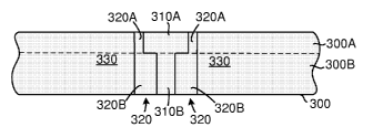
WO 2006/123298 PCT/IB2006/051566
2
this regard, through-wafer interconnection has been proven to be a powerful
technique.
In addition, through-wafer interconnection allows wafer-level processing that
results in
simultaneous fabrication of large number of packages. This advantage limits
the
additional packaging cost that might have incurred due to the high complexity
of the
technology. It also avoids of the long wires running in or across the wafer
surface and
thus reduces the undesired parasitic capacitance and high interconnection
resistance.
[9] Most through-wafer connections are done with through-wafer vias or holes,
which
are filled with a connective material. A prior art through-wafer interconnect
is shown
in FIG. 1. The through-wafer interconnect is built in a via through a
substrate 10 by
first making a hole 12, then forming a seed layer 14 on surfaces of the hole
12 and sub-
sequently forming a metal layer 16 (e.g., using electroplating methods) on the
seed
layer 14. The metal layer 16 serves as a through-wafer conductor to
electrically
connect devices or connectors (not shown) on one side of the substrate 10 to
devices or
connectors on the other side. In a typical application, devices are on the top
side of the
substrate 10. The through-wafer conductor (metal layer 16) connects the
devices to a
connector (such as a connection pad or connection ball) on the backside.
[10] The fabrication process of the above-shown through-wafer interconnections
is
usually complex and requires rather sophisticated technologies. The
fabrication process
also lacks freedom for design optimizations. For example, the thickness of the
metal
layer 16 as shown in FIG. 1 is inherently limited by the existing
electroplating
techniques. The resultant through-wafer interconnects also lacks physical
flexibility. It
is therefore desirable to introduce new designs of through-wafer
interconnection to
improve the fabrication process and the performance of through-wafer
interconnects.
Summary of the Invention
[11] This application discloses a through-wafer interconnect and a method for
fabricating the same. Unlike existing methods which make through-wafer in-
terconnects by forming a via in a wafer and introducing a conductive material
into the
via (e.g., by electroplating, thin film deposition, etc.), the invention
method takes a
reversed approach by starting with a conductive wafer, for example a highly
doped
silicon wafer, to form a through-wafer conductor from the native material of
the
conductive wafer.
[12] One aspect of the present invention is a method for fabricating through-
wafer in-
terconnects in a microelectronic structure. The method comprises the steps of
(1)
providing a conductive wafer having a front side and a backside; (2) forming a
patterned trench by removing material of the conductive wafer, wherein the
patterned
trench has an annular circumferential opening generally dividing the
conductive wafer
along the opening into an inner portion and an outer portion whereby the inner
portion
of the conductive wafer is insulated from the outer portion and serves as a
through-
CA 02607885 2007-11-07
WO 2006/123298 PCT/IB2006/051566
3
wafer conductor. A dielectric material may be added into or formed in the
patterned
trench to mechanically connect the conductors and the surrounding structures
together.
[13] Various shapes are suitable for the patterned trench. For example, the
patterned
trench may have different cross-sectional sizes (such as a diameter) at two
portions at
different depths of the wafer. In one embodiment, the through-wafer conductor
has a
bottom portion surrounded and defined by a bottom portion of the patterned
trench and
a top portion surrounded and defined by a top portion of the patterned trench.
The
bottom portion of the through-wafer conductor has a smaller cross-sectional
size than
the top portion of the through-wafer conductor.
[14] The through-wafer conductor may be formed in a conductive layer that has
two
contiguous sections or a conductive wafer that has a top layer and a bottom
layer
which are two separate layers bonded together. In another embodiment, the
conductive
wafer is a doped silicon wafer that has a top section and a bottom section
having
different doping levels. In a preferred embodiment, the bottom portion of the
patterned
trench has trench openings broader than that of the top portion, whereby a
bottom
portion of the through-wafer conductor surrounded and defined by the bottom
portion
of the patterned trench has a smaller cross-sectional size than a top portion
of the
through-wafer conductor surrounded and defined by the top portion of the
patterned
trench.
[15] In one embodiment, the method has additional steps of forming a first
portion of the
patterned trench from one of the front side or the backside and forming a
second
portion of the patterned trench from the other side. The first portion of the
patterned
trench may be oxidized to form a stop layer thereon to define a stop position
for the
forming of the second portion of the patterned trench stops. A dielectric
material may
be added into or formed in at least one of the first and the second portions
of the
patterned trench.
[16] In another embodiment, at least a portion of the patterned trench is
further fine-
patterned within the trench openings with open passages interlined with lines
of
unremoved conductive wafer material. The lines of unremoved conductive wafer
material may be oxidized to achieve the effect of adding a dielectric
material. Al-
ternatively or additionally, a filler material may be added between the
oxidized lines of
unremoved conductive wafer material. In another embodiment, a first dielectric
material is added into a top portion of the patterned trench and a second
dielectric
material is added into a bottom portion of the patterned trench.
[17] The lines of unremoved conductive wafer material may be patterned to form
a
framework between the inner portion and the outer portion of the conductive
wafer to
connect and support the two portions. In one embodiment, at least part of the
lines of
unremoved conductive wafer material is completely oxidized such that the
framework
CA 02607885 2007-11-07
WO 2006/123298 PCT/IB2006/051566
4
is electrically insulative between the inner portion and the outer portion of
the
conductive wafer. In another embodiment, a filler material is added into the
trench, and
at least part of the lines of unremoved conductive wafer material is then
etched away
such that the framework is electrically insulative between the inner portion
and the
outer portion of the conductive wafer.
[18] The method may be used to form a plurality of patterned trenches
similarly char-
acterized. The plurality of patterned trenches may be arranged side-by-side in
an array
with neighboring patterned trenches sharing a common trench side, or with
neighboring patterned trenches separated by an intervening spacing. The
intervening
spacing may be occupied by a conductive material for decoupling neighboring
conductors. The conductive material in the intervening spacing may be an
unremoved
native conductive material of the conductive wafer.
[19] In one embodiment of the fabrication method, the conductive wafer is a
conductive
silicon wafer, and the patterned trench may be formed using semiconductor
fabrication
methods. An exemplary fabrication method includes the steps of (1) forming a
top
portion of the patterned trench by etching from the front side of the
conductive silicon
wafer; (2) forming an oxide layer over surfaces of the top portion of the
patterned
trench; (3) removing at least part of the oxide layer on a bottom of the top
portion of
the patterned trench; (4) forming an enlarged cavity at the bottom of the top
portion of
the patterned trench by isotropic silicon etching; forming a stop layer for
backside
silicon etching by oxidizing a bottom surface of the enlarged cavity; and (5)
forming a
bottom portion of the patterned trench by etching from the backside of the
conductive
silicon wafer to the stop layer.
[20] Another aspect of the invention is a method for fabricating through-wafer
in-
terconnects in a microelectronic structure by bonding two conductive wafers
together.
The method comprising the steps of: (1) bonding a first conductive wafer and a
second
conductive wafer such that a bottom side of the first conductive wafer
contacting a top
side of the second conductive wafer; (2) forming a top portion of a patterned
trench
through a top side of the second conductive wafer by removing material of the
first
conductive wafer; (3) forming a bottom portion of the patterned trench through
the
backside of the first conductive wafer to connect with the top portion. The
first portion
and the second portion of the patterned trench each have an annular
circumferential
opening generally dividing the respective conductive wafer into an inner
portion and
an outer portion. The inner portion of the respective conductive wafer is
insulated from
the outer portion of the respective conductive wafer, and the inner portion of
the first
conductive wafer and the inner portion of the second conductive wafer are
electrically
connected to serves as a through-wafer conductor.
[21] In one embodiment, before bonding the second conductive wafer, a cavity
is formed
CA 02607885 2007-11-07
WO 2006/123298 PCT/IB2006/051566
on the top side of the first conductive wafer, and at least a bottom surface
of the cavity
is oxidized to form an etch stop layer thereon. A bottom portion of the
patterned trench
is then formed by etching through the backside of the first conductive wafer
to the etch
stop layer.
[22] The second conductive wafer may be either pre-fabricated to contain at
least part of
a microelectronic device or allows fabricating a microelectronic device after
bonding
to the first conductive wafer. For the latter, after bonding the second
conductive wafer,
at least a part of a microelectronic device may be fabricated on the second
conductive
wafer. A metal layer may be then deposited on top of the second conductive
wafer and
patterned.
[23] In a preferred embodiment to minimize parasitic capacitance, the bottom
portion of
the patterned trench has trench openings broader than that of the top portion
of the
patterned trench, whereby a bottom portion of the through-wafer conductor
surrounded
and defined by the bottom portion of the patterned trench has a smaller cross-
sectional
size than a top portion of the through-wafer conductor surrounded and defined
by the
top portion of the patterned trench.
[24] In another preferred embodiment, the bottom portion of the patterned
trench is
further fine-patterned within the trench openings with open passages
interlined with
lines of unremoved conductive wafer material. The lines of unremoved
conductive
wafer material may be patterned to form a framework between the inner portion
and
the outer portion of the conductive wafer to connect and support the two
portions. At
least a part of the lines of unmoved conductive wafer material may be totally
oxidized
or etched away after adding another dielectrical material into the trench.
[25] Another aspect of the invention is a through-wafer interconnect which
provides
electrically conductive interconnection between electric contacts on a front
side and a
backside of a wafer in a microelectronic structure. The through-wafer
interconnect
comprises: (1) a through-wafer conductor passing through the front side of the
wafer to
the backside of the wafer; (2) an insulator surrounding at least a main body
portion of
the conductor; and (3) a frame surrounding the through-wafer conductor and the
insulator. At least a portion of the through-wafer conductor and a respective
surrounding portion of the frame each have a native material of the wafer. In
one
embodiment, at least a portion of the conductor and a respective surrounding
portion of
the frame have a common native material of the wafer. The wafer is preferably
a
conductive wafer.
[26] The insulator may be a dielectric material added to an annular trench
formed in the
wafer by removing native material of the wafer. For example, an oxide may be
formed
on lines of unremoved native material of the wafer patterned in the annular
trench. Al-
ternatively or additionally, a filler material may be filled between lines of
unremoved
CA 02607885 2007-11-07
WO 2006/123298 PCT/IB2006/051566
6
native material of the wafer patterned in the annular trench.
[27] In one embodiment of the through-wafer interconnect, the frame has a
zigzag
shaped wall which is flexible through stretching or compressing.
[28] Another aspect of the present invention is a through-wafer interconnect
component
that has: (1) a plurality of conductors arranged in an array, each conductor
passing
through a front side of a conductive wafer to a backside of the conductive
wafer; (2) an
insulator surrounding each conductor; and (3) a frame supporting the plurality
of
conductors and the insulator. At least a portion of each conductor and a
portion of the
frame each have a native material of the conductive wafer. In one embodiment,
the
insulator is disposed in a plurality of annular trenches each surrounding a
respective
conductor. The annular trenches are formed by removing native material of the
conductive wafer. In one embodiment, the frame has an outer peripheral wall
and a
plurality of inter-conductor walls; the outer peripheral wall device defines a
general
area where the plurality of conductors and the insulator are disposed; and a
plurality of
inter-conductor walls divide the general area into a plurality of sub-areas
each
containing a conductor and a respective portion of the insulator surrounding
the
conductor. The inter-conductor walls of the frame may comprise a conductive
material
to function as a decoupling conductor between the plurality of conductors.
[29] The unique design of the present invention allows for a flexible through-
wafer in-
terconnect with a frame having a zigzag shaped wall which is flexible through
stretching or compressing.
[30] The present invention avoids the conventional procedure of introducing a
conductor
to the wafer to make a through-wafer interconnect. Instead, the present
invention
allows using the native conductive material of a conductive wafer to form a
through-
wafer conductor. The conductor is insulated from the rest of the wafer using
insulators
that can be formed using standard semiconductor fabrication processes. The
method
introduces greater engineering freedom for designing the shape of the
conductor to
minimize parasitic capacitance, the shape and properties of the insulator, and
the shape
and mechanical properties of the overall through-wafer interconnect. When used
on a
silicon wafer, for example, the method can take advantage of semiconductor
fabrication and micromachining for creating various shapes and structures. In
contrast,
the conventional methods are limited by the dimensions and shapes of via holes
and
the thickness thin films formed by processes such as thin-film deposition,
oxidation, or
electroplating.
[31] The method and the through-wafer interconnects in accordance with the
present
invention have applications in a broader range of technologies. It is
particularly useful
for assembling and packaging microelectronic devices such as microelectronic
imagers
used in digital cameras and wireless devices with picture capabilities,
micromachined
CA 02607885 2007-11-07
WO 2006/123298 PCT/IB2006/051566
7
ultrasonic transducers, micromirror arrays for optical communication, optical
displays,
etc.
[32] The foregoing and other features and advantages will become more apparent
from
the following detailed description of several embodiments, which proceeds with
reference to the accompanying figures.
Description of Drawings
[33] FIG. 1. shows a prior art through-wafer interconnect.
[34] FIG. 2 shows a schematic cross-sectional view of a through-wafer
interconnect in
accordance with the present invention.
[35] FIG. 3 shows a schematic cross-sectional view of another through-wafer in-
terconnect in accordance with the present invention.
[36] FIGS. 4A-4C show schematics of a through-wafer interconnection design
having
multiple conductors.
[37] FIG. 4D is a variation of FIG. 4C.
[38] FIGS. 5A-5C show schematics of another through-wafer interconnection
design
having multiple conductors.
[39] FIG. 5D shows a cross-sectional view of a variation of the through-wafer
inter-
connection structure in FIGS. 5A-5C.
[40] FIG. 6 shows a bottom review of a flexible through-wafer interconnection
structure
in accordance with the present invention. FIG. 7 shows an example of the
insulator
surrounding the through-wafer interconnection conductor in accordance with the
present invention.
[41] FIG. 8 shows an example of a modified conductor in accordance with the
present
invention.
[42] FIG. 9 shows an example of a modified decoupling conductor in accordance
with
the present invention.
[43] FIGS. 10.1-10.5 show a process flow of a first exemplary fabrication
method.
[44] FIG. 10.4A shows an alternative step in the process of the first
exemplary
fabrication method.
[45] FIG. 10.3B shows a bottom view of an exemplary trench pattern design in
the
through-wafer interconnect structure at the step shown in FIG. 10.3.
[46] FIG. 10.3C shows a bottom view of another exemplary trench pattern design
in the
through-wafer interconnect structure at the step shown in FIG. 10.3.
[47] FIGS. 11.1-11.2 show an exemplary thin silicon line having segments that
are
completely oxidized.
[48] FIGS. 12.1-12.7 show a process flow of a second exemplary fabrication
method.
[49] FIGS. 13.1-13.8 show a process flow of a third exemplary fabrication
method.
[50] FIGS. 14.1-14.6 show a process flow of a fourth exemplary fabrication
method.
CA 02607885 2007-11-07
WO 2006/123298 PCT/IB2006/051566
8
[51] FIG. 14.2A shows an alternative step in the process of the first
exemplary
fabrication method.
[52] FIG. 14.4B shows a bottom view of the through-wafer interconnect
structure at the
step shown in FIG. 14.4.
[53] FIGS. 15.1A-15.8 show a process flow of a fifth exemplary fabrication
method.
[54] FIGS. 15.1B, 15.2B and 15.3B show top views of the through-wafer inter-
connection at steps shown in FIG. 15.1A, FIG. 15.2A, and FIG. 15.3A,
respectively.
DETAILED DESCRIPTION
[55] The through-wafer interconnection in accordance with the present
invention for will
be described in detail along with the figures, in which like parts are denoted
with like
reference numerals or letters.
[56] In this document, the words 'circular' and 'annular' only suggest in the
broadest
sense that a shape has a looped form, a curved shape that is nearly looped, or
an ar-
rangement that is generally shaped like a ring, and do not suggest a rounded
shape or
any other shape in particular, nor does it suggest that the loop or ring is
entirely
complete or unbroken.
[57] FIG. 2 is a schematic cross-sectional view of a through-wafer
interconnect in
accordance with the present invention. The through-wafer interconnect is built
in a
wafer 200. The through-wafer interconnect includes a conductor 210 passing
through
the front side (top) of the wafer 200 to the backside (bottom) of the wafer.
The
conductor 210 is surrounded by an insulator 220, and both the conductor 210
and the
insulator 220 are surrounded by a frame 230. The through-wafer interconnect in
accordance with the present invention is characterized in that at least a
portion of the
conductor 210 and a respective surrounding portion of the frame 230 each
comprise a
native material of the wafer 200. As will be shown more clearly in the context
of
fabrication methods described herein, this means that the conductor 210 may be
fabricated directly out of the wafer 200 if the wafer 200 is made of a
conductive
material.
[58] In this document, a conductive material is defined as one having a
resistivity less
than 1 x 10⁴ Q-cm. As will be shown in the description of the fabrication
methods, one
particularly useful conductive material for fabricating a through-wafer
interconnect of
the present invention is doped silicon wafers.
[59] Because the conductor 210 is conductively accessible from both the front
side (top)
and the backside (bottom) of the wafer 200, with proper connectors (not shown)
the
through-wafer interconnect in accordance with the present invention provides
electrically conductive interconnection between electric contacts on the front
side and
the backside of the wafer 200. This has many applications in a broader range
of
technologies. It is particularly useful for assembling and packaging
microelectronic
CA 02607885 2007-11-07
WO 2006/123298 PCT/IB2006/051566
9
devices such as microelectronic imagers used in digital cameras and wireless
devices
with picture capabilities, micromachined ultrasonic transducers, micromirror
arrays for
optical communication, optical displays, etc.
[60] For example, a microelectronic device (not shown) may be placed or
fabricated
directly on the front side (top) of the wafer 200 and connected to an
integrated circuit
(not shown) which is located on the front side of the wafer 200. The
integrated circuit
is then connected to the conductor 210 through an electric contact (not
shown). The
conductor 210 itself may be connected to another electric contact (not shown)
on the
backside of the wafer 200. In principle, any device that requires, or may be
benefited
by, a through-wafer interconnect may use the through-wafer interconnect in
accordance with the present invention.
[61] Opposite to the prior art concept of through-wafer interconnection, the
conductor
210 in the through-wafer interconnect of the present invention may be made of
a native
material of the conductive wafer 200, instead of being made of an external
conductive
material introduced to a hole or a via in the wafer. The insulator 220 may be
made of
one or more insulating materials (such as a dielectric material) added to a
void space
formed from the wafer 200. Because of its unique design, the invention confers
a great
level of freedom in designing and fabricating the shape, size, electrical and
mechanical
properties of the conductor 210, the insulator 220 and the frame 230. For
example, the
dimensions of the conductor 210 are no longer limited by thin-film deposition
or elec-
troplating techniques as in the prior art through-wafer interconnection
designs. If the
overall conductivity of the conductor 210 needs to be higher, for instance,
the re-
quirement may be satisfied by increasing the cross-sectional size (thickness)
of the
conductor 210.
[62] As will be shown further below, the above described basic concept of the
present
invention may be applied in the great number of variations.
[63] FIG. 3 shows a schematic cross-sectional view of another through-wafer in-
terconnect in accordance with the present invention. This is a more specific
embodiment of the general concept illustrated in FIG. 2. The conductor 310 now
has a
top portion 310A and a bottom portion 310B. The bottom portion 310B has a
smaller
cross-sectional size than the top portion 310A, resulting in a smaller
electric contact
area on the backside and thus reducing parasitic capacitance. The insulator
320 has a
first portion 320A surrounding the top portion 310A of the conductor 310 and a
second
portion 320B surrounding the bottom portion 310B of the conductor 310.
Similarly,
the through-wafer interconnect has a frame 330 surrounding the conductor 310
(310A
and 310B) and the insulator (320A and 320B).
[64] It is appreciated that either the top portion 310A of the conductor or
the bottom
portion 3 10B of the conductor, or both the top portion 3 10A and the bottom
portion
CA 02607885 2007-11-07
WO 2006/123298 PCT/IB2006/051566
310B may have a native conductive material of the wafer 300. Correspondingly,
a
respective surrounding portion of the frame 330 may also have the same native
conductive material of the wafer 300. It is further appreciated that the wafer
300 may
either be a monolithic wafer or include a top section 300A corresponding in
depth to
the top portion 310A of the conductor and a bottom section 300B corresponding
to the
bottom portion 310B of the conductor. The top section 300A and the bottom
section
300B may be just two different sections of a single contiguous wafer (wafer
300). For
example, the wafer 300 may be a doped conductive silicon wafer, with the top
section
300A and the bottom section 300B having different doping levels.
Alternatively, the
top section 300A and the bottom section 300B may be two separate layers bonded
together to form a composite wafer 300. The two separate layers (300A and
300B) of
the wafer 300 may be either directly bonded together without an intervening
layer or
indirectly bonded with an intervening layer. In a configuration in which the
two
separate layers 300A and 300B are indirectly bonded together with an
intervening
layer sandwiched there between, it is essential that the conductivity from the
top
portion 310A of the conductor to the bottom portion 300B is not interrupted.
[65] The basic design of through-wafer interconnection in accordance with the
present
invention may be used for fabricating through-wafer interconnect structures
that are
more complicated.
[66] FIGS. 4A-4C show schematics of a through-wafer interconnection design
having
multiple conductors. FIG. 4A shows a top view of the design, FIG. 4B shows a
bottom
view of the design, and FIG. 4C shows a cross-section view of the design
through the
dashed line in FIG. 4A and FIG. 4B.
[67] The through-wafer interconnection structure is built in a conductive
wafer 400 and
has an array of four conductors 410, 412, 414 and 416 each passing through the
front
side (top) of a conductive wafer 400 to a backside (bottom) of the conductive
wafer
400. The through-wafer interconnection structure further has a patterned
insulator
having a top portion 420A and the bottom portion 420B. The insulator (420A and
420B) passes through a front side of the conductive wafer 400 to the backside
of the
conductive wafer 400. The insulator surrounds each conductor 410, 412, 414 and
416.
A frame 430 supports the conductors 410, 412, 414 and 416 and the insulator
(420A
and 420B). Similar to the through-wafer interconnect shown in FIGS. 2-3, the
through-
wafer interconnection structure in FIGS. 4A-4C is characterized in that at
least part of
each conductor 410, 412, 414 and 416 and at least a portion of the frame 430
each
comprise a native material of the conductive wafer 400, allowing the
conductors 410,
412, 414 and 416, and at least a part of the frame 430 to be fabricated
directly from the
conductive wafer 400.
[68] The conductors 410, 412, 414 and 416 are used to access the devices (not
shown)
CA 02607885 2007-11-07
WO 2006/123298 PCT/IB2006/051566
11
on the front surface (top) of the wafer 400 from the backside (bottom) of the
wafer
400.
[69] Still referring to FIGS. 4A-4C, it is shown that conductors 410, 412, 414
and 416
each have a top portion (410A, 412A, 414A and 416A, respectively) and a bottom
portion (410B, 412B, 414B and 416B, respectively). The bottom portions 410B,
412B,
414B and 416B each have a smaller cross-sectional size than the respective top
portion
410A, 412A, 414A and 416A. The top portions (410A, 412A, 414A and 416A) of the
conductors 410, 412, 414 and 416 correspond to the top portion 420A of the
insulator
in a top section 400A of the conductive wafer 400. The bottom portions (410B,
412B,
414B and 416B) of the conductors 410, 412, 414 and 416 correspond to the
bottom
portion 420B of the insulator in a bottom section 400B of the conductive wafer
400.
Accordingly, the bottom portion 420B has a greater cross-sectional size than
the
respective top portion 420A.
[70] In FIG. 4C, it is shown that the two sections 400A and 400B belong to the
same
contiguous monolithic single wafer 400. The two sections 400A and 400B may be
of
an identical material, but may also be of the same wafer material having
different
doping levels.
[71] An alternative configuration is shown in FIG. 4D, where top portions
410A, 412A,
414A and 416A and the bottom portions 410B, 412B, 414B and 416B belong to two
separate layers, namely a top layer 401A and a bottom layer 401B, that are
bonded
together to form a composite wafer 400. It is appreciated the two separate
layers 401A
and 401B may either the bonded together directly as shown in FIG. 4D or bonded
indirectly through an intervening material (not shown).
[72] Where the wafer 400 is made of the top layer 401A and the bottom layer
401B, the
top portions of the conductor and the top portion of the insulator may be
formed in the
top layer 401A, while the bottom portions of the conductor and the bottom
portion of
the insulator may be formed in the bottom layer 401B. In addition to the
difference in
the cross-sectional sizes, the top portion of the conductor and the bottom
portion of the
conductor may also be made of different materials. Likewise the top portion of
the
insulator and the bottom portion of the insulator may also be made of
different
materials. It is appreciated that many variations or modifications can be made
based on
the basic design illustrated herein. The only requirement is that the
conductivity path
along the conductors 410, 412, 414 and 416 between the top side and the bottom
side
of the wafer 400 is maintained.
[73] In FIGS. 4A-4D and other figures below, an array of four identical
conductors is
used to demonstrate the interconnection design. However, it is appreciated
that the
through-wafer interconnection design can be used of for any number of devices,
any
array of devices, any array of through-wafer conductors, or multiple arrays
with
CA 02607885 2007-11-07
WO 2006/123298 PCT/IB2006/051566
12
different number of devices and conductors, and any other configurations that
may
require or may benefit from through-wafer interconnection. In addition,
although the
cross sections of the conductors, the insulator and the frame have a square
shape in the
examples shown, it is appreciated that these parts can be of any geometric
shapes as
long as the arrangement thereof provides the desired through-wafer
interconnection in
accordance with the present invention.
[74] FIGS. 5A-5C show schematics of another through-wafer interconnection
design
having multiple conductors. FIG. 5A shows a top view of the design, FIG. 5B
shows a
bottom view of the design, and FIG. 5C shows a cross-section view of the
design
through the dashed line in FIG. 5A and FIG. 5B.
[75] The through-wafer interconnection structure in FIGS. 5A-5C is similar to
that in
FIGS. 4A-4C. The through-wafer interconnection structure is built in a
conductive
wafer 500 and has an array of four conductors 510, 512, 514 and 516 each
passing
through the front side (top) of a conductive wafer 500 to a backside (bottom)
of the
conductive wafer 500. The through-wafer interconnection structure further has
a
patterned insulator assembly that has insulators 520, 522, 524 and 526 each
surrounding a corresponding conductor 510, 512, 514 and 516, and a frame 530
me-
chanically supporting the conductors 510, 512, 514 and 516 and the insulator
assembly
(insulators 520, 522, 524 and 526). Similar to the through-wafer interconnect
shown in
FIGS. 2-3 and FIGS. 4A-4C, the through-wafer interconnection structure in
FIGS.
5A-5C is characterized in that at least part of each conductor 510, 512, 514
and 516
and at least a portion of the frame 530 each comprise a native material of the
conductive wafer 500, allowing the conductors 510, 512, 514 and 516, and at
least a
part of the frame 530 to be fabricated directly from the conductive wafer 500.
[76] It is also shown in FIGS. 5A-5C that conductors 510, 512, 514 and 516
each have a
top portion (510A, 512A, 514A and 516A, respectively) and a bottom portion
(510B,
512B, 514B and 516B, respectively). The bottom portions 510B, 512B, 514B and
516B each have a smaller cross-sectional size than the respective top portion
510A,
512A, 514A and 516A. This allows a large interconnection contact area through
the
top portions 510A, 512A, 514A and 516A of the through-wafer conductors without
having to result in an overly large through-wafer conductor to causes
undesired effects
such as high parasitic capacitance.
[77] It is appreciated that top portions 510A, 512A, 514A and 516A and the
bottom
portions 510B, 512B, 514B and 516B may either belong to different sections of
the
same contiguous single wafer 500 or belong to two separate layers that are
bonded
together to form a composite wafer 500. The two separate layers may either the
bonded
together directly or bonded indirectly through an intervening material (not
shown).
[78] Unlike the through-wafer interconnection structure in FIGS. 4A-4C, the
through-
CA 02607885 2007-11-07
WO 2006/123298 PCT/IB2006/051566
13
wafer interconnect of FIGS. 5A-5C has a slightly more sophisticated frame 530.
The
frame 530 has an outer peripheral wa11530a and a plurality of inter-conductor
walls
530b. The outer peripheral walls 530a define a general area where the
conductors 510,
512, 514 and 516 and the insulator assembly of insulators 520, 522, 524 and
526 are
disposed, while the plurality of inter-conductor walls 530b further divide the
general
area into a plurality of sub-areas each containing one of the conductors 510,
512, 514
and 516 and a respective surrounding portion of the insulator assembly
(insulators 520,
522, 524 and 526, respectively, in the example) surrounding the conductor.
[79] The inter-conductor walls 530b of the frame 530 may also have a
conductive
material to function as a decoupling conductor between the plurality of
conductors
510, 512, 514 and 516. The conductive material may also be a native material
of the
conductive wafer 500, thus allowing the decoupling conductor (the inter-
conductor
walls 530b of the frame 530) to be fabricated, together with the through-wafer
conductors 510, 512, 514 and 516, from the conductive wafer 500. The
decoupling
conductor may be connected to a certain voltage source (DC or AC). The
decoupling
design is useful in the through-wafer interconnection designs shown herein
because
electrical AC signals may couple between conductors through insulation
material.
Placing a conductive layer or wall such as the decoupling conductor 530b
between the
conductors 510, 512, 514 and 516 helps to shield the electric coupling between
these
conductors.
[80] FIG. 5D shows a cross-sectional view of a variation of the through-wafer
inter-
connection structure in FIGS. 5A-5C. In FIG. 5D, the inter-conductor walls
531b are
lower than the outer peripheral wa11530a and only extend across the lower
portion of
the wafer 500.
[81] For some special applications, the transducers may need to connect to a
flexible
through-wafer connection. The flexible through-wafer connection can be
realized by
thinning the thickness of the connection. However, with the unique design of
the
through-wafer interconnection of the present invention, the parts along the
through-
wafer connection (conductors, insulators and the frame) may be designed as a
flexible
structure by virtue of its shape instead of its thinness alone.
[82] FIG. 6 shows a bottom review of a flexible through-wafer interconnection
structure
in accordance with the present invention. The through-wafer interconnection
structure
in FIG. 6 is similar to that in FIGS. 5A-5C. If the cross-sectional view is
taken from
the dashed line indicated, it would look like the cross-sectional view showing
in FIG.
5C. The frame 630 has outer peripheral walls 630-1, 630-2, 630-3 and 630-4
that
define a general area where the conductors 610, 612, 614 and 616 (shown bottom
portions 610B, 612B, 614B and 616B) and the insulator assembly of insulators
620,
622, 624 and 626 are disposed. The frame 630 also has inter-conductor walls
630-5
CA 02607885 2007-11-07
WO 2006/123298 PCT/IB2006/051566
14
and 630-6 that further divide the general area into sub-areas each containing
one of the
conductors 610, 612, 614 and 616 and a respective portion of the insulator
assembly
(insulators 620, 622, 624 and 626, respectively, in the example) surrounding
the
conductor.
[83] Unlike the through-wafer interconnection structure in FIGS. 5A-5C, walls
630-2,
630-4 and 630-6 of the frame 630 are made of thin segments and have a zigzag
shaped.
These thin and zigzag shaped walls provide a degree of flexibility through
stretching or
compressing. Such flexibility can be particularly helpful when the through-
wafer inter-
connection structure is used for fabricating and packaging microelectronic
devices that
have a movable part, or have a part that is subject to bending.
[84] As will be more clearly illustrated in the descriptions of fabrication
methods, the
insulator or insulators in the through-wafer interconnects shown above in
FIGS.
4A-4C, FIGS. 5A-5D and FIG. 6 are disposed in annular trenches each
surrounding a
respective conductor. The annular trenches are formed by removing the native
material
of the conductive wafer. The insulators may include a dielectric material
added to the
annular trench.
[85] FIG. 7 shows an example of the insulator surrounding the through-wafer
inter-
connection conductor in accordance with the present invention. The insulator
720 is
disposed in an annular trench formed on the wafer (not shown) and constitutes
lines
740 of unremoved native material of the wafer interlined with spaces 745. The
lines
740 of unremoved native material are formed when the annular trench is formed
using
a patterned material removal method such as patterned etching method (details
shown
in the description of fabrication methods herein below). The lines 740 of
unremoved
native material may form a supporting framework between conductors (e.g.
conductors
410 and 412 in FIGS. 4A-4C) and their surrounding frame (e.g., the frame 430
in
FIGS. 4A-4C). To ensure electrical insulation by the insulator 720, the lines
740 of
unremoved native material of the wafer may be oxidized. To further ensure
electrical
insulation, at least part of the lines 740 of unremoved native material may be
completely oxidized such that the supporting framework formed by the lines 740
is
sufficiently insulative between the conductor and the frame (which may also be
a part
of a conductive wafer and therefore conductive). Alternatively or
additionally, a
dielectric filler material may be added to fill the spaces 745 between lines
740 of
unremoved native material.
[86] FIG. 8 shows an example of a modified conductor in accordance with the
present
invention. Although initially made from the native material of the wafer, the
conductor
may be further modified to be partially different from the original native
material of
the wafer. As shown in FIG. 8, conductor 810 has a top portion 810A and a
bottom
portion 8 10B. Part of the native material of the original wafer in the bottom
portion
CA 02607885 2007-11-07
WO 2006/123298 PCT/IB2006/051566
810B is removed from a bottom end 810C to form spaces 845 between lines 840 of
unremoved native material. A new material may be then introduced to this
partially
hallowed structure to modify the physical properties of the conductor 810. For
example, the lines 840 may be oxidized to form oxidation, or covered by a new
material. Additionally or alternatively, spacings 850 may be filled with
another
material.
[87] Modification similar to that shown in FIG. 8 with respect to the through-
wafer
conductor may also be made to a decoupling conductor (e.g., 530b in FIGS. 5A-
5C).
FIG. 9 shows an example of a modified decoupling conductor in accordance with
the
present invention. An exemplary decoupling conductor 930 has a top portion
930A and
a bottom portion 930B. Part of the native material of the original wafer in
the bottom
portion 930B is removed from a bottom end 930C to form spaces 945 between
lines
940 of unremoved native material. A new material may be then introduced to
this
partially hallowed structure to modify the physical properties of the
decoupling
conductor 930. For example, the lines 940 may be oxidized to form oxidation,
or
covered by a new material. Alternatively, spaces 945 may be filled with
another
material.
[88] The conductors described herein can be made of the any conductive
material. One
good choice is to form the conductors using semiconductor wafers (e.g.
silicon, GaAs,
etc). Heavily doped semiconductor wafer may be used to improve the
conductivity. As
discussed in FIGS. 4A-4D, FIGS. 5A-5D, and FIG. 6-9, the through-wafer
conductors
may be made of the two portions. A top portion is used to connect the devices
on the
front surface of the wafer. The shape of the top portion of each conductor is
usually
determined by the dimensions and shapes of the devices which connect to the
through-
wafer interconnections. For example, the top portion of the conductor can
serve as one
of the electrodes of capacitance micromachined ultrasonic transducers (cMUTs).
The
bottom portion of the conductor is designed with a trade-off between the
capacitance
and resistance of the interconnection. The capacitance increases with the
perimeter
length of the conductor. A through-wafer conductor of a greater cross-
sectional size
(i.e., thicker) this means greater parasitic capacitance. On the other hand,
the resistance
decreases with the cross-sectional size of the conductor. A balance is struck
to
optimize the performance.
[89] The top portion of the insulator and the bottom portion of the insulator
may be
made of either the same material or different materials, and both can be made
of any
kind of medium or material, including but not limited to vacuum, air, silicon,
oxide,
nitride, SOG, TEOS, polyimide, polymer, rubber, PDMS, PMMA, epoxy, gel, and
any
filling material for ultrasonic transducers, or a combination thereof. In
order to ensure
good insulation, however, a useful combination should result in an insulator
that is
CA 02607885 2007-11-07
WO 2006/123298 PCT/IB2006/051566
16
non-conductive as a whole. When a combination of different materials is used
in a
portion (top portion or bottom portion) of the insulator, preferably at least
one material
is an insulation material. In addition, a configuration of the insulator
should desirably
provide the mechanical strength to the wafer so that the wafer or the devices
can
survive during the device fabrication process and device assembly and
packaging.
[90] As will be shown in the fabrication methods described herein, the through-
wafer
connection can be controlled to a desired thickness using grinding and
polishing of the
processed wafer in a certain fabrication step. Usually, a thicker through-
wafer
connection is preferred for easier and more reliable fabrication process and
packaging
handling, but a thinner through-wafer connection is usually desired to improve
the
device performance. A balance often needs to be struck. However, the conflict
may be
at least partially avoided by a carefully designed fabrication process. For
example, the
wafer thinning can be done before, after or during the fabrications of the
through-wafer
connection. If the thickness of the wafer is too thin to be handled during the
process,
the thin wafer with through-wafer connections may be bonded or stuck to
another
wafer using a proper wafer bonding technique or a proper stiction layer. Using
this
technique, the resultant bonded wafer as a whole may be robust enough to be
processed.
[91] Besides the electric properties, other parameters in the design of the
through-wafer
connection may also be considered to meet the special needs of the particular
device
which connects to the through-wafer connection. For example, for the IR
sensors, the
thermal conductive and a thermal capacitance are important parameters. For an
inertial
sensor, the through-wafer interconnection may be designed to be insensitive to
the
vibration coupling from the environment. For an ultrasonic transducer,
materials
selections and the structure configurations of the through-wafer
interconnection should
be used to achieve certain acoustic properties. For example, the
interconnection should
provide acoustic decoupling between the cMUT elements and absorb the acoustic
energy leaked into the substrate from the transducers. The through-wafer inter-
connection in the present invention provides the flexibility to select many
different
materials and to design the conductors, insulators and decouple conductors
with
different shapes and configurations to achieve the desired performance.
[92] Fabrication Methods of the Through-wafer Interconnection
[93] A variety of fabrication methods may be used to make the through-wafer
inter-
connections in accordance with the present invention. The fabrication of the
through-
wafer interconnections may be done before or after the device fabrication
process.
Furthermore, the fabrication of the through-wafer interconnections may be
integrated
with the device fabrications.
[94] The choice of the fabrication methods is dependent on the material
compatibility
CA 02607885 2007-11-07
WO 2006/123298 PCT/IB2006/051566
17
and process compatibility (e.g., the process thermal budget, the etch
selectivity, wafer
surface topography and the wafer rigidity, etc.) of both the device
fabrication and the
through-wafer interconnection fabrication. The process method and the
materials used
should be carefully evaluated at each fabrication step, with consideration to
factors
such as process temperature, to ensure compatibility. This is especially
important when
the fabrications of the device and the interconnection are integrated.
[95] Described below are some exemplary fabrication methods for the through-
wafer in-
terconnection of the present invention. Silicon wafer is used in these
examples for the
purpose of illustration. However, the methods of fabrication, including
material and p
rocess selections, are not limited by the illustrative examples.
[96] Individual steps taken should be interpreted broadly in the context of
its intended
purpose. For example, the phrase 'adding a material' does not mean that the
material
added must be an external material. It is appreciated that the material may be
either al-
ternatively or additionally added by a process of forming a new material, such
as
oxidation. Furthermore, the thinning process is not shown in the examples of
the
process flows below. It is appreciated that in the wafer thinning process can
be
performed before and/or during the fabrication process.
[97] Some fabrication methods described below show a degree of integration of
the
device fabrication and the through-wafer interconnection fabrication. However,
it is
appreciated that the interconnection fabrication methods may or may not be
integrated
with the device fabrications.
[98] Moreover, the through-wafer interconnection may be fabricated by
combining some
steps or changing the step orders of different fabrication methods described
herein.
[99] (1) Fabrication method I:
[100] FIGS. 10.1-10.5 show a process flow of a first exemplary fabrication
method. FIG.
10.4A shows an alternative step in the process. FIG. 10.3B shows a bottom view
of the
through-wafer interconnect structure after the step shown in FIG. 10.3. The
process
flow is outlined in the following steps.
[1011 In step one (FIG. 10.1), patterned top trenches 1010 are formed on
silicon wafer
1000 by silicon etching to define the top portions 1020 of the through-wafer
conductors and the top portion of inter-conductor frame 1025. An example of
the inter-
conductor frame 1025 is illustrated as inter-conductor wa11530b in FIGS. 5A-
5D. It is
however appreciated that a similar process may be used to fabricate a through-
wafer
interconnection without inter-conductor frame 1025 (such as that shown in
FIGS.
4A-4D).
[102] Viewed from the top of the silicon wafer 1000, patterned top trenches
1010 would
show an annular circumferential opening similar to that illustrated in the top
views
FIG. 4A and FIG. 5A. In this document, the term 'annular' means the opening is
CA 02607885 2007-11-07
WO 2006/123298 PCT/IB2006/051566
18
generally shaped like a ring, but does not suggest any particular shape of the
ring, nor
does it suggest that the ring is entirely complete or unbroken.
[103] As shown in exemplary top views such as FIG. 4A and FIG. 5A, the annular
top
trenches 1010 generally divide the silicon wafer 1000 along the trench opening
into an
inner portion and an outer portion whereby the inner portion of the silicon
wafer will
serve as a through-wafer conductor of the through-wafer interconnect being
made.
[104] In step two (FIG. 10.2), a thermal oxidation 1030 (or LTO, nitride,
etc.) is grown
over top trenches 1010 to form an etch stop layer 1040 for backside silicon
etch in the
next step. Additionally or alternatively, a filler material (not shown) may be
added into
trench 1010 if needed. The filler material may be an external material or
formed by
oxidation of unremoved native material in the trench 1010. The backside
silicon etch
will define the shape of the bottom portions of the conductors.
[105] In step three (FIG. 10.3), backside silicon etch is performed to form
bottom
trenches 1060. The overall pattern of bottom trenches 1060 defines the bottom
portions
of the through-wafer conductors 1050. In the particular example illustrated,
bottom
trenches 1060 are not entirely devoid of the wafer material. Instead, each
bottom
trench 1060 is fine-patterned within the trench openings with open passages
(gaps or
spaces) 1045 interlined with thin silicon lines 1065 of unremoved conductive
wafer
material. The shape, size and spacing of the fine pattern within the bottom
trenches
1060 is not limited to any particular model, as long as it does a meaningful
mod-
ification of the properties of an empty trench or a proper preparation for the
next step.
[106] In step four (FIG. 10.4), the fine-pattern of the thin silicon lines
1065 are oxidized.
Optionally (FIG. 10.4A), open passages 1045 between the thing silicon lines
1065 may
be filled with a filler material 1055 without oxidizing the silicon lines
1065. The filler
material 1055 may be an oxide, PDMS, SOG or another material for achieving a
desired electric or mechanical property.
[107] In step five (FIG. 10.5), if the thing silicon lines 1065 are oxidized
in the above step
four, optionally the open passages 1045 between the thing silicon lines 1065
can still
be filled with a filler material 1055, which may be an oxide, PDMS, SOG or
another
material for achieving a desired electric or mechanical property.
[108] Preferably the thin silicon lines 1065 are designed so that the thin
lines 1065 can be
oxidized, the spaces (open passages 1045) can be filled, and the stress
induced by the
oxidation minimized.
[109] Two exemplary designs of the patterned thin silicon lines 1065 are
illustrated in
FIG. 10.3B and 10.3C which show the bottom view of the silicon wafer 1000 at
the
end of step 3 (FIG. 10.3). The pattern shown in FIG. 10.3 B will continue with
the st
eps shown in FIG. 10.4 and 10.5. The pattern shown in FIG. 10.3C will continue
with
the step shown in FIG. 10.4A. Many other possible patterns and a variety of
different
CA 02607885 2007-11-07
WO 2006/123298 PCT/IB2006/051566
19
thicknesses of the silicon lines may be used. The patterns should desirably
provide
enough mechanical strength for the wafer during the fabrication and packaging
processes. For example, the lines of unremoved conductive wafer material may
form a
framework between the inner portion (conductor 1050) and the outer portion
(frame
1005) of the conductive wafer to connect and support the two portions.
[110] Preferably, at least a part of the thin silicon lines 1065 or a segment
of some of the
thin silicon lines 1065 in the fine-pattern are thin enough so that it can be
completely
oxidized to form insulation between conductors. FIGS. 11.1-11.2 show an
exemplary
thin silicon line having segments that can be completely oxidized. FIG. 11.1
shows
thin silicon line 1100 before oxidation. FIG. 11.2 shows the thin silicon line
1100 after
oxidation where segments 1110 and 1120 are completely oxidized.
[1111 Moreover, the pattern may be designed to minimize the stress built
during the
oxidation process and, if needed, to be easily filled by selected material
(e.g. LTO,
SOG, TEOS, nitride, polyimide, polymer, rubber, PDMS, PMMA, epoxy, gel, etc)
with desired properties. Finally, the pattern itself may be designed to have
desired
properties particularly pertinent to the device supported by the through-wafer
inter-
connection. For example, the pattern may be designed to achieve a certain
acoustic
impedance is the through-wafer interconnection is used for supporting a mi-
cromachined ultrasound transducer. In addition, if needed, the patterned
structure can
be design to be flexible in the desired direction.
[112] The device fabrication (e.g., cMUT fabrication) may be started after the
oxidation
step (the step three). The through-wafer connections shown in this example can
be
carried out either before or during the device fabrication.
[113] Furthermore, after step two (FIG. 10.2), a filler material (preferably
insulative) may
be added into the top trench 1010. With this procedure, it is possible that
the insulative
material within the top trench 1010 itself can provide enough strength to hold
the
conductors (or wafers) sturdy enough during the process. In this case, the
shape and the
inner pattern of the trench 1060 may not need to be designed to form a
framework to
support and to connect the conductors. An example is shown in FIG. 10.3C. Ac-
cordingly, electrical insulation between the conductors may be achieved by
simply
adding an insulative filler material into trenches, instead of using oxidation
of the fine
patterns in the patterned trenches.
[114] Furthermore, through-wafer interconnection fabrication method in this
example can
be done with a reversed sequence by forming the bottom trench 1060 first, then
ending
with the top trench formation 1010 and a dielectric material filling (no
shown).
[115] (2) Fabrication Method II:
[116] FIGS. 12.1-12.7 show a process flow of a second exemplary fabrication
method.
The process flow is outlined in the following steps.
CA 02607885 2007-11-07
WO 2006/123298 PCT/IB2006/051566
[117] In step one (FIG. 12.1), top trenches 1210 are etched on silicon wafer
1200. Oxide
1220 is grown over the cavities 1210. Oxide 1220 is patterned so that only the
oxide in
top trenches 1210 is kept as etch stop 1225 of the backside silicon etch in a
subsequent
step.
[118] In step two (FIG. 12.2), a second wafer 1230 is bonded to silicon wafer
1200 over
the top of top trenches 1210. Wafer 1230 is ground to a desired thickness for
forming
the top portion of a conductor. The layer 1230 may also be taken from a
silicon layer in
a SOI wafer.
[119] In step three (FIG. 12.3), a device 1235 (e.g., a cMUT) is fabricated on
or above the
second wafer 1230 to a stage that the fabricated device still allows high
temperature
process if the oxidation is needed later. The device 1235 is represented by a
simple box
without showing details or the exact location. The fabrication of the device
1235 may
be finished at this step if there is no more subsequent high temperature
process steps.
Second wafer 1230 may serve as an electric contact, such as a bottom
electrode, of the
device 1235.
[120] In step four (FIG. 12.4), patterned bottom trenches 1240 are formed
using backside
etch to define the bottom portions 1250 of the conductors. Patterned bottom
trenches
1240 have patterned lines 1265 of the unremoved native material of silicon
wafer 1200
interlined or spaced from each other by gaps or spaces 1245. It is appreciated
that any
pattern of lines 1265 and spaces 1245, such as that shown in FIG. 10.3B or
10.3C, may
be designed and used, depending on the desired process and properties.
[1211 In step five (FIG. 12.5), patterned bottom trenches 1240 are oxidized to
make
insulation between the conductors 1250. Preferably, at least the part of the
silicon lines
1265 defined in previous silicon etch step (step four) is completely oxidized.
More
preferably, all of the silicon lines 1265 are completely oxidized. The
oxidation also
forms in oxide layer 1270 over the bottom portions 1250 of the through-wafer
conductor, as well as bottom portions of the outer frame 1205 and inter-
conductor
frame 1255.
[122] At step four (FIG. 12.4), if the layer 1230 and the device 1235 can
provide enough
strength to hold the conductors (or wafers) to survive the process, the shape
and the
pattern of the trench 1240 may not need to be designed to serve such a
purpose. For
example, the trench 1240 may be designed to cut through the wafer to achieve
the
electric insulation between the conductors and the frames directly (such as
the pattern
shown in FIG. 10.3C). Therefore, the oxidation step (step five, FIG. 12.5) may
not be
necessary to form insulation between conductors. Nevertheless, a fill material
may still
be added into the void within the trench if needed to finish the process.
[123] In step six (FIG. 12.6), gaps or spaces 1245 in the patterned bottom
trenches 1240
are filled using a material 1260 with desired properties. Vias are opened on
the oxide
CA 02607885 2007-11-07
WO 2006/123298 PCT/IB2006/051566
21
1270 on the bottom surface of the bottom portions 1250 of the through-wafer
conductors to access the conductors. After that, a metal layer 1280 with
desired
properties is deposited and patterned. A hard mask may be used to form the
metal
pattern on the backside of the through-wafer interconnection if the voids
between the
conductors are not going to be refilled after that.
[124] In step seven (FIG. 12.7), fabrication of the device 1235 on the front
surface is
completed, and top portions 1252 of the conductors are further defined by
silicon etch.
[125] It is appreciated that in this method, as well as other methods
described herein,
some steps (such as oxidation and adding a filling material) are optional.
This is not
limited to just those specifically indicated as being optional in the
description.
[126] (3) Fabrication method III:
[127] FIGS. 13.1-13.8 show a process flow of a third exemplary fabrication
method. This
method is similar to the above second method except for using a different
technique to
define the etch stop for the backside silicon etch which defines the bottom
part of the
conductors. The process flow is outlined in the following steps.
[128] In step one (FIG. 13.1), top trenches 1310 are etched on silicon wafer
1300. Oxide
1320 is grown over the top trenches 1310. The oxide at the bottom 1322 of the
top
trenches 1310 is then removed.
[129] In step two (FIG. 13.2), isotropic silicon etch is performed to form
cavities 1324.
The surface of the cavities 1324 created by the isotropic silicon etch is
oxidized to
form a stop layer 1325 for backside silicon etch. If desired, the trench 1310
may be
field with a filler material (not shown) in this step.
[130] In step three (FIG. 13.3), the device 1330 (e.g., a cMUT) is fabricated
on or above
the wafer 1300 to a stage that the fabricated device still allows high
temperature
process if the oxidation is needed later. The fabrication of device 1330 may
be finished
at this step if there is no more subsequent high temperature process step.
[131] The process from step four to step eight (FIGS.13.4-13.8) is similar to
the process
described from step four (FIG.12.4) to step seven (FIG.12.7) in the
fabrication method
II. In these figures, the patterned bottom trenches 1340, patterned lines 1365
of the
unremoved native material of the silicon wafer 1300, spaces 1345, bottom
portions
1350 of the through-wafer conductor, inter-conductor frame 1355, filler
material 1360,
oxide layer 1370, metal layer 1380, and the top portions 1352 of the
conductors, are
similar to their equivalents in the fabrication method II.
[132] It is again appreciated that in this method, as well as other methods
described
herein, some steps are optional.
[133] (4) Fabrication Method IV:
[134] FIGS. 14.1-14.7 show a process flow of a fourth exemplary fabrication
method. The
process flow is outlined in the following steps.
CA 02607885 2007-11-07
WO 2006/123298 PCT/IB2006/051566
22
[135] In step one (FIG. 14.1), the same processes as described in the first
three steps of
the above fabrication method II shown in FIG. 12.1, FIG. 12.2 and FIG. 12.3
are first
performed on silicon wafer 1400. Top trenches 1420 and backside etch stop
layer 1425
are formed in these steps. The fabrication process of the device 1490 may also
be
completed at this stage.
[136] In step two (FIG. 14.2), patterned bottom trenches 1440 are formed using
backside
etch to define the bottom portions 1450 of the through-wafer conductors.
Patterned
bottom trenches 1440 has patterned lines 1465 of the unremoved native material
of
silicon wafer 1400 interlined or spaced from each other by gaps or spaces
1445. It is
appreciated that any pattern of lines 1465 and spaces 1445 may be designed and
used,
depending on the desired process and properties. In this step, inter-conductor
frame
1455, which may serve as a decoupling conductor, may also be formed if
desired.
[137] In addition, in step two backside etching may also be performed on the
frame 1405,
the inter-conductor frame 1455, and the bottom portions 1450 of the through-
wafer
conductors to further modify the structure and properties of the conductors.
This
technique may be used to achieve some desired effects for the particular type
of device
that is being fabricated and packaged using the through-wafer interconnection
technique. For example, special patterns may be etched, materials may be
added, and
oxidation performed in the etched patterns in order to achieve special
acoustic
properties if the device is a micromachined ultrasonic transducer (MUT).
[138] An example of this extra backside etching shown and wafer modification
is il-
lustrated in FIG. 14.2A, which is an alternative of the cross-sectional view
FIG. 14.2 in
step two but with additional etching. It is appreciated that this extra
fabrication steps
can be incorporated into other fabrication methods in similar ways.
[139] In step three (FIG. 14.3), gaps or spaces 1445 in the patterned bottom
trenches 1440
are filled using a material 1460 with desired properties.
[140] In step four (FIG. 14.4), the whole or part of silicon pattern in the
bottom trenches
1440 is etched to make isolation between conductors 1450 and the conductive
frame
(1405 and 1455). For example, at least a part of the previously unremoved
silicon lines
1465 may be now removed to form avoids (spaces) 1466. As discussed in step
two, the
bottom portions 1450 of the through-wafer conductors and the conductive frames
(outer frame 1405 and inter-conductor frame 1455) can also be etched into a
desired
pattern in this step, if such etching has not been performed already in a
previous step
(e.g., step two).
[1411 FIG. 14.4B is a bottom view after the step four.
[142] In step five (FIG. 14.5), avoids 1466 created from the silicon etch at
step four is
filled using a material or materials 1467 with desired properties. This step
is optional.
A metal layer 1480 is then deposited and patterned on the bottom surface of
the
CA 02607885 2007-11-07
WO 2006/123298 PCT/IB2006/051566
23
through-wafer conductors and the conductive frames.
[143] In step six (FIG. 14.6), the device fabrication is completed on the
wafer surface, and
the top portions 1452 of the through-wafer conductors are further defined by
etching
from the top side of the wafer.
[144] Compared with the fabrication methods 1-3, the fabrication methods 4
does not use
high temperature process of thermal oxidation to make insulation between the
conductors and the conductive frame. Instead, the whole or part of the silicon
pattern
between the conductors is etched to achieve the insulation between them (see
step
four). For this reason, at least one material with desired properties should
be used to
fill the gaps or spaces within silicon pattern created by the backside silicon
etching
which also defines the bottom portions of the through-wafer conductors. In
contrast, in
the fabrication methods 1-3 the step to fill the gaps within the oxide pattern
is entirely
optional.
[145] The above fabrication method IV may also be combined with the
fabrication
methods I-III such that the resultant method is substantially similar to the
fabrication
method IV except that top trenches 1420 and backside etch stop layer 1425 are
formed
differently.
[146] As in other fabrication methods described herein, wafer thinning can be
performed
if needed. A hard mask may be used to form the metal pattern on the backside
of the
through-wafer interconnection if the voids between the conductors are not to
be filled.
[147] (5) Fabrication Method V:
[148] FIGS. 15.1-15.8 show a process flow of a fifth exemplary fabrication
method.
FIGS. 15.1B, 15.2B and 15.3B show top views of the through-wafer
interconnection at
a respective step. The process flow is outlined in the following steps.
[149] In step one (FIG. 15.1A and FIG. 15.1B), deep silicon etching is
performed from
the front side of the wafer 1500 to a desired thickness to form deep trenches
1511 with
silicon patterns 1512, which can be oxidized to form insulation between the
conductors. If desired, etch may go through the entire wafer 1500. Recesses
1513 on
silicon surface can be etched first if needed. FIG. 15.1A is a cross-sectional
view of
this formation, while FIG. 15.1B is the top view of the same. The exemplary
silicon
pattern shown here is designed to minimize the oxide volume and the thermal
stress
effects in the structure. Other patterns may be used as long as they can be
oxidized and
form insulation between the conductors after finishing the fabrication.
[150] In step two (FIG. 15.2A and FIG. 15.2B), the silicon patterns 1512
formed in the
previous step is oxidized to form an oxide formation 1514. FIG. 15.2A is a
cross-
sectional view of this formation, while FIG. 15.2B is the top view of the
same.
[151] In step three (FIG. 15.3A and FIG. 15.3B), patterned annular deep
trenches 1541
are formed. FIG. 15.3A is a cross-sectional view of this formation, while FIG.
15.3B is
CA 02607885 2007-11-07
WO 2006/123298 PCT/IB2006/051566
24
the top view of the same. The annular deep trenches 1541 have unremoved
silicon
lines 1543 and empty spaces (voids) 1542, together forming a framework between
the
frame 1505 and conductors 1550. The annular deep trenches 1541 will insulate
the
conductors and define the bottom portions of the conductors. A thin oxide may
be
grown to form a stop layer for late process.
[152] In step four (FIG. 15.4), a prime wafer 1551 is bonded to the patterned
wafer 1500
over recesses 1513 and is ground and polished to a desired thickness. The
layer 1551
may also obtained by bonding with an SOI wafer.
[153] In step five (FIG. 15.5), the prime wafer 1551 is patterned and etched
to form the
top portions 1552 of the conductors. Step five is optional.
[154] In step six (FIG. 15.6), devices 1535 are fabricated. A etch process may
be
performed to define the top part of the conductors.
[155] In step seven (FIG. 15.7), the wafer 1500 is ground (and polished if
needed), or
etched, to reach the bottom of the annular deep trenches 1541 from the
backside of the
wafer. If an etch stop layer was formed at the bottom of the annular deep
trenches 1541
in a previous step, the backside etching stops at the etch stop layer.
[156] In step eight (FIG. 15.8), voids 1545 in the silicon pattern are filled
with a desired
material 1560 if needed. A metal layer 1580 is then deposited and patterned on
the
backside of the wafer.
[157] If the through-wafer interconnection is used for a cMUT, the top
portions 1552 of
the through-wafer conductors may serve as the substrate, as well as the bottom
electrode, of the cMUT. A hard mask may be used to form the metal pattern on
the
backside of the through-wafer interconnection if the voids between the
conductors are
not to be refilled.
[158] There is a broader range of applications of the through-wafer
interconnection of the
present invention. In general, it can be used for miniaturization of
electronic
components such as ICs, microelectronic devices used in sensor arrays,
transducer
arrays, and photo imager arrays, and modules that are used in portable devices
like
cellular phones and PDAs. The application of the present invention helps to
avoid long
wires running in or across the wafer surface and thus reduces the undesired
parasitic
capacitance and high interconnection resistance. The invention thus
facilitates the re-
alization of ultimate miniaturization in reaching chip size packaging (CSP) of
the
components. This could potentially result in a more efficient fabrication
process,
reduced foot print of the components on the printed board, greater fill
factor, and can
also improve the device performance. In particular, the design of the present
invention
can be used for devices that have vertical discrete components and stacked
planar dies
where the conventional rerouting methods are insufficient. The fabrication
methods of
through-wafer interconnection of the present invention allow wafer-level
processing
CA 02607885 2007-11-07
WO 2006/123298 PCT/IB2006/051566
that results in simultaneous fabrication of large number of packages.
[159] One exemplary envisioned application of the through-wafer
interconnection is in
micromechanical smart sensor and actuator systems, including but not limited
to photo
imagers used in digital cameras and cell phones, micromachined ultrasonic
transducers
(MUTs such as cMUTs, pMUTs and mMUTs), and micromirror array. Such systems
are often realized as a multi-wafer device in which the mechanical functions
are
distributed over different wafers and one of the wafers is dedicated to
contain the
readout circuits. The individually processed wafers can be assembled using
wafer-
to-wafer bonding and can be combined to one single functional
electromechanical unit
using the through-wafer interconnect of the present invention, provided that
the
processes involved comply with the constraints imposed by the proper operation
of the
active electrical and the micromechanical systems.
[160] In particular, the through-wafer interconnection technology according to
the present
invention may be used in fabricating and packaging the novel MUTs (especially
cMUTs) disclosed in international patent applications (PCT) 'METHODS FOR
FABRICATING MICRO-ELECTRO-MECHANICAL DEVICES', attorney Docket
No. 03004.02; 'MICRO-ELECTRO-MECHANICAL TRANSDUCERS', attorney
Docket No. 03004.03; and 'MICRO-ELECTRO-MECHANICAL TRANSDUCERS',
attorney Docket No. 03004.04, all filed on even date with the present patent
ap-
plication by the common applicant. These patent applications are hereby
incorporated
herein by reference in their entirety.
[161] In the foregoing specification, the present disclosure is described with
reference to
specific embodiments thereof, but those skilled in the art will recognize that
the present
disclosure is not limited thereto. Various features and aspects of the above-
described
disclosure may be used individually or jointly. Further, the present
disclosure can be
utilized in any number of environments and applications beyond those described
herein
without departing from the broader spirit and scope of the specification. We
claim all
such modifications and variations that fall within the scope and spirit of the
claims
below. The specification and drawings are, accordingly, to be regarded as
illustrative
rather than restrictive. It will be recognized that the terms 'comprising,'
'including,' and
'having,' as used herein, are specifically intended to be read as open-ended
terms of art.