Note: Descriptions are shown in the official language in which they were submitted.
CA 02607916 2007-11-07
WO 2006/123300 PCT/IB2006/051568
Description
MICRO-ELECTRO-MECHANICAL TRANSDUCERS
[1] This application claims priority from United States Provisional
Applications Serial
No. 60/682,619, filed May 18, 2005; Serial No. 60/692,038, filed June 17,
2005; Serial
No. 60/705,606, filed August 3, 2005; and Serial No. 60/744242, filed Apri14,
2006,
which applications are incorporated herein by reference in their entirety.
[2] This application further incorporates herein by reference in entirety the
following:
[3] International Application (PCT), entitled THROUGH-WAFER INTER-
CONNECTION (Attorney Docket No. 03004.01), filed on even date with the present
application by the common applicant;
[4] International Application (PCT), entitled METHODS FOR FABRICATING
MICRO-ELECTRO-MECHANICAL DEVICES (Attorney Docket No. 03004.02),
filed on even date with the present application by the common applicant; and
[5] International Application (PCT), entitled MICRO-ELECTRO-MECHANICAL
TRANSDUCERS (Attorney Docket No. 03004.04), filed on even date with the
present
application by the common applicant.
Technical Field
[6] The present invention relates to micro-electro-mechanical devices that
have a
movable mechanical part for energy transformation, particularly to
micromachined
ultrasonic transducers (MUT) such as capacitance micromachined ultrasonic
transducers (cMUT).
Background Art
[7] Micro-electro-mechanical transducers usually share a common feature which
includes a movable mechanical part used for energy transformation. One example
of
such micro-electro-mechanical transducers is micromachined ultrasonic
transducers
(MUT). An ultrasound transducer performs a chain of energy transformation to
realize
its function of a transducer. In its receiving mode, the acoustic energy of
ultrasound
waves propagating in a medium where the transducer is placed is transformed to
mechanical energy of a movable part (conventionally a vibrating membrane) in
the
transducer. The motion of the movable part is then transformed to a detectable
elec-
tromagnetic (usually electrical) signal. In its transmitter mode, the reverse
chain of
energy transformation takes place.
[8] Various types of ultrasonic transducers have been developed for
transmitting and
receiving ultrasound waves. Ultrasonic transducers can operate in a variety of
media
including liquids, solids and gas. These transducers are commonly used for
medical
imaging for diagnostics and therapy, biochemical imaging, non-destructive
evaluation
of materials, sonar, communication, proximity sensors, gas flow measurements,
in-situ
CA 02607916 2007-11-07
WO 2006/123300 PCT/IB2006/051568
process monitoring, acoustic microscopy, underwater sensing and imaging, and
many
others. In addition to discrete ultrasound transducers, ultrasound transducer
arrays
containing multiple transducers have been also developed. For example, two-
dimensional arrays of ultrasound transducers are developed for imaging
applications.
[9] Compared to the widely used piezoelectric (PZT) ultrasound transducer, the
MUT
has advantages in device fabrication method, bandwidth and operation
temperature.
For example, making arrays of conventional PZT transducers involves dicing and
connecting individual piezoelectric elements. This process is fraught with
difficulties
and high expenses, not to mention the large input impedance mismatch problem
presented by such elements to transmit/receiving electronics. In comparison,
the micro-
machining techniques used in fabricating MUTs are much more capable in making
such arrays. In terms of performance, the MUT demonstrates a dynamic
performance
comparable to that of PZT transducers. For these reasons, the MUT is becoming
an
attractive alternative to the piezoelectric (PZT) ultrasound transducers.
[10] Among the several types of MUTs, the capacitive micromachined ultrasonic
transducer (cMUT), which uses electrostatic transducers, is widely used. Other
MUTs
using piezoelectric (pMUT) and magnetic (mMUT) transducers are also adopted.
Examples of prior art cMUT structure are shown in FIGS. lA-1C, FIGS. 2-3, and
FIGS. 4A-4B.
[11] FIG. 1A shows a cross-sectional view of a basic structure of a prior art
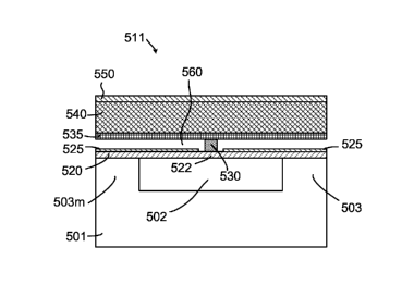
cMUT
having multiple cells. FIG. 1B shows an enlarged view of a single cMUT cell
10. FIG.
1C shows a corresponding schematic top view of the same prior art multi-cell
cMUT
structure. In practice, a functional cMUT may have at least one independently
ad-
dressable cMUT element. Based on the conventional design, each cMUT element
consists of many cMUT cells which are connected in parallel. Four cells are
shown in
FIG. 1A, a single cell is shown in FIG. 1B, and ten cells are shown in FIG.
1C, but all
cells belong to a single cMUT element in FIGS. lA-1C.
[12] The cMUT of FIGS. 1A-1C is built on a substrate 11. As shown in a
selected
cMUT cell 10, each cMUT cell has a parallel plate capacitor consisting of a
rigid
bottom electrode 12 and a top electrode 14 residing on or within a flexible
membrane
16 that is used to transmit or receive an acoustic wave in the adjacent
medium. The
flexible membrane 16 in each cell is supported by the insulation wall or posts
18. The
membrane 16 is spaced from the substrate 11 and the top electrode 12 to define
a
transducing space 19 therebetween. A DC bias voltage is applied between the
electrodes 12 and 14 to deflect the membrane 16 to an optimal position for
cMUT
operation, usually with the goal of maximizing sensitivity and bandwidth.
During
transmission an AC signal is applied to the transducer. The alternating
electrostatic
force between the top electrode and the bottom electrode actuates the membrane
16 in
CA 02607916 2007-11-07
WO 2006/123300 PCT/IB2006/051568
order to deliver acoustic energy into the medium (not shown) surrounding the
cMUT.
During reception the impinging acoustic wave vibrates the membrane 16, thus
altering
the capacitance between the two electrodes. An electronic circuit detects this
ca-
pacitance change.
[13] Alternatively the membrane can be actuated and the displacement of the
membranes
detected using a piezoelectric transducer (pMUT) and a magnetic transducer
(mMUT).
FIG. 2 shows a pMUT ce1120 which has a similar structure to the cMUT cell 10
except
that the capacitor (electrodes 12 and 14) are replaced by a piezoelectric
member 24 on
the membrane 26. FIG. 3 shows a mMUT ce1130 which has a similar structure to
the
cMUT cell 10 except that the capacitor (electrodes 12 and 14) are replaced by
a
magnetic member 34 on the membrane 36.
[14] Methods of fabrication for making a cMUT shown in FIGS. 1 A-1 C have been
developed. Exemplary methods are disclosed in U.S. Patent Nos. 6,632,178 and
6, 958,
255.
[15] There are drawbacks in the cMUTs of the prior art structures and methods.
Many of
these drawbacks relate to the fact that each addressable cMUT element is made
of
many individual cells and each cell has its cMUT membrane clamped or fixed on
edges shared by the adjacent cells. Examples of the drawbacks are listed
below.
[16] (1) The average displacement of the membranes is small because of the
clamped
edges. As a result both the device transmission and reception performance are
poor.
[17] (2) Surface areas occupied by the clamped areas (e.g., edges) and the
walls or posts
are non-active, thus reducing the device fill factor and the overall
efficiency.
[18] (3) Anchor areas introduce a parasitic capacitance which decreases the
device
sensitivity.
[19] (4) The anchor pattern within the surface of the cMUT element may cause
ultrasonic wave interference which limits the device bandwidth.
[20] (5) The non-uniform displacement of the membrane may disturb the
ultrasonic
wave pattern. For example, the non-uniform displacement may affect the
ultrasonic
beam pattern emitted from the transducer surface and also cause acoustic cross
coupling through the transducer surface.
[21] (6) The resonant frequencies of individual cells in the same cMUT element
may be
different between each other because of the process variation. This causes
phase
differences of the membrane motion among different cells in the same cMUT
element
during operation. As a result, the sum of the average displacement of the cMUT
element may degrade dramatically. This problem degrades the device performance
especially when the cMUT works in a high quality factor (Q-factor) condition,
for
example in air.
[22] (7) The acoustic energy can couple into the transducer substrate through
supporting
CA 02607916 2007-11-07
WO 2006/123300 PCT/IB2006/051568
walls and cause undesired effects such as acoustic cross coupling between the
cMUT
elements. An effort to reduce the cross-coupling through the substrate by
introducing
materials with desired acoustic properties may require occupation of extra
space
between elements.
[23] The above problems also exist in the pMUT and mMUT of the prior art since
they
have a similar structure as the cMUT as shown in FIG. 1.
[24] Another cMUT device having a compliant support structure built on the
substrate to
support the membrane is disclosed in the U.S. Patent No. 7,030,536. A cMUT
according to that design is shown in FIGS. 4A-4B. FIG. 4A shows cross-
sectional view
of a single cMUT ce1140 as disclosed in that patent. FIG. 4B shows the
schematic top
view of multiple cMUT cells as disclosed in that patent. Compared to the
conventional
cMUT structure shown in FIGS. lA-1C, the cMUT structure disclosed in U.S.
Patent
No. 7,030,536 uses a compliant support structure 48 in place of the
conventional
insulation wall 18 to define the perimeter ends of the membrane 46 of each
cMUT cell
40, such that the top electrode 44 and the membrane 46 may move in a piston-
like
manner. This has potential advantages but the design according to the patent
also
introduces its own problems, as will be discussed in view of the present
invention in
the detailed description.
[25] Due to the importance of these MUT devices, it is desirable to improve
the
technology in terms of performance, functionality, and manufacturability.
SUMMARY OF THE INVENTION
[26] This application discloses a micro-electro-mechanical transducer (such as
a cMUT)
that has a movable mechanical part to transform energy. The transducer has a
substrate, a top plate, and a resilient structure therebetween. The resilient
structure has
multiple connectors distributed over the device element area to vertically
transport the
top player with distributed support not limited to edges. The resilient
structure may be
cantilevers, or cantilever-containing structures such as bridges or crossbars,
formed
using a middle spring layer covering cavities on the substrate. Connectors
define a
transducing space below the top plate. The resilient structure such as
cantilevers enable
a vertical displacement of the connectors, which transports the top plate in a
piston-like
motion to change the transducing space and to effectuate energy
transformation. No
separate cells are necessary for each addressable transducer element. Multiple
device
elements can be made on the same substrate.
[27] According to one aspect of the invention, a micro-electro-mechanical
transducer is
characterized in that:
[28] (a) the resilient structure has a lower portion connecting to the
substrate and an
upper portion connecting to the top plate layer;
[29] (b) the upper portion of the resilient structure has a plurality of
connectors
CA 02607916 2007-11-07
WO 2006/123300 PCT/IB2006/051568
connecting to the top plate layer;
[30] (c) the plurality of connectors are distributed over the device element
area and have
at least one connector located substantially away from the device element
periphery
toward an inner region of the device element area;
[31] (d) a transducing space is defined below the top plate layer;
[32] (e) the addressable device element has at least one transducing member to
induce
energy transformation; and
[33] (f) the resilient structure enables a vertical displacement of the
plurality of
connectors to transport the top plate layer in a substantially vertical
direction, thus
changing the transducing space and activating the transducing member.
[34] In one embodiment, the resilient structure has a middle spring layer
placed over the
substrate. The middle spring layer and the substrate define at least one
cavity inside the
device element area. The cavity divides the device element area into at least
two
opposing sides, at least one side having an anchor anchoring the middle spring
layer.
The plurality of connectors are each horizontally distanced from the anchor by
a
sufficient length to define a cantilever or a bridge between the connector and
the
anchor. In this embodiment, each connector may have a desired height and stand
from
the top of the middle spring layer to separate the top plate from the middle
spring layer
to define the transducing space below the top plate layer.
[35] In one preferred embodiment, the substrate and the middle spring layer
define a
plurality of cavities dividing the device element area into segments each
substantially
smaller than the device element area. Multiple cantilevers or bridges may be
defined
over the plurality of cavities to provide a distributed support to the top
plate layer.
[36] In one embodiment, the cavities and the corresponding anchors together
occupy at
least half the device element area. Within the device element area the middle
spring
layer may be a contiguous layer covering the top surface of the anchor. In one
embodiment, the contiguous middle spring layer covers at least half of the
device
element area, and preferably the contiguous middle spring layer covers
substantially
the entire device element area.
[37] In one embodiment, the cavity has an annular shape dividing the substrate
wafer
into an inner island and an outer region, and the inner island constitutes the
anchor.
The anchor may include a first anchor comprising the inner island and an
opposing
second anchor comprising the outer region.
[38] In one embodiment the cavity comprises a first plurality of extended
cavities
forming a pattern of cavities and anchors on the substrate wafer. Various
patterns may
be formed.
[39] The cantilevers may be of a variety of formations. For example, the
cavity may be
defined by at least two anchors opposing each other, and the middle spring
layer within
CA 02607916 2007-11-07
WO 2006/123300 PCT/IB2006/051568
the device element area may connect to both opposing anchors. The connector
may be
located between the two opposing anchors and horizontally distanced from each
of the
two opposing anchors by a sufficient length to define two cantilevers
connected head-
to-head at a location where the connector is positioned. For another example,
the
anchor may define a circular sidewall surrounding the cavity, the middle
spring layer
may cover the entire cavity, and the connector may be at a position directly
above a
middle area of the cavity to define a two-dimensional plane cantilever.
[40] One aspect of the invention is a micro-electro-mechanical transducer
wherein the
middle spring layer has a plurality of connectors connecting to the top plate
layer. The
plurality of connectors is distributed across the device element area to
define a
connector density profile having an average connector density per area
location. Each
cantilever thus formed has a spring strength, which when combined with the
respective
average connector density defines an effective spring intensity profile in
which the
effective spring intensity is the spring strength per area location. The
effective spring
intensity may either be substantially uniform over the device element area or
have a
nonuniform distribution profile. For example, the effective spring intensity
may be sig-
nificantly higher at area locations near a center of the device element area
than
locations near a perimeter of the device element area.
[41] In one embodiment having multiple connectors, the device element area
comprises
two regions having different thicknesses of the top plate layer and different
spring in-
tensities. For example, a first region may have a greater thickness of the top
plate layer
and great effective spring intensity than the second region, or vice versa. In
another
embodiment the device element area comprises a perimeter surrounding a middle
region, wherein the top plate layer is flexible near the parameter but rigid
in the middle
region, clamped at a perimeter sidewall and supported by at least one
cantilever in the
middle region.
[42] The micro-electro-mechanical transducer may have additional
characteristics. For
example, the addressable device element the top plate layer may have a
thickness
profile having at least two different thicknesses across the device element
area. The
two different thicknesses may comprise a first thickness corresponding to a
normal
thickness of the top plate layer and a second thickness corresponding to a
bottom
thickness of a cavity formed on the top plate layer, the first thickness and
the second
thickness regularly alternating across the device element area. For another
example,
the addressable device element the top plate layer may comprise a first
material and a
second material different from the first material. In one embodiment, the
first material
has a plurality of segments divided by separation trenches and the second
material
spans over the segments to connect the segments of the first material. The
second
material may also at least partially fill the separation trenches.
CA 02607916 2007-11-07
WO 2006/123300 PCT/IB2006/051568
[43] In one embodiment, the micro-electro-mechanical transducer is a
capacitance mi-
cromachined ultrasonic transducer (cMUT), wherein each addressable device
element
has a top electrode on the top plate layer and a bottom electrode on either
the middle
spring layer or the substrate wafer. Example, the middle spring layer may
comprise a
conductive material to effectuate as the bottom electrode. Alternatively, the
top
electrode may be a separate conductive layer deposited on the top plate layer.
[44] In another embodiment, the micro-electro-mechanical transducer has a
plurality of
addressable device elements, which may be separated by a separation trench
formed
through at least part of the top plate layer. The substrate wafer may be a
conductive
wafer, and the addressable device element is insulated by an embedded
insulator
formed on the substrate wafer. The embedded insulator comprises an insulation
cavity
having a desired overall thickness and being filled with a dielectric
material. Al-
ternatively, the addressable device element is insulated by an embedded
insulator
formed on the substrate wafer, the embedded insulator comprising a patterned
cavity
containing solid lines of oxidized native material of the substrate wafer. The
embedded
insulator may also be formed on the top plate layer.
[45] In one embodiment, the addressable device element is addressed from the
back side
of the substrate wafer via a through-wafer interconnect formed through the
substrate
wafer. For example, a conductive substrate wafer may be used, and the through-
wafer
interconnect may include an annular trench surrounding a through-wafer
conductor
made of a native material of the conductive wafer. A dielectric material may
be used to
fill the annular trench to insulate the through-wafer conductor from the rest
of the
substrate wafer. In one particular configuration, the through-wafer conductor
is
positioned directly underneath the addressable device element.
[46] The micro-electro-mechanical transducer may also be a pMUT, wherein the
transducing member comprises a piezoelectric member disposed on the middle
spring
layer or the top plate layer. The micro-electro-mechanical transducer may also
be a
mMUT, wherein the transducing member comprises a magnetic member disposed on
the middle spring layer or the top plate layer.
[47] The performance of the micro-electro-mechanical transducer may be
enhanced by
careful selection of the top plate material or configuration. For example, the
top plate
layer may have holes formed therethrough. The holes may have a size and
location
profile that optimizes a rigidity/mass ratio of the top plate layer.
Furthermore, in order
to avoid electric shorting problem, the maximum vertical displacement of the
connector may be limited to be no greater than, preferably less than, the
height of the
transducing space between the top plate layer and the top surface of the
anchor
including any intervening layer. In one embodiment, the maximum vertical dis-
placement of the connector is limited by a motion stopper disposed in the
cavity.
CA 02607916 2007-11-07
WO 2006/123300 PCT/IB2006/051568
[48] According to another aspect of the invention, a micromachined ultrasonic
transducer (MUT) structure has a substrate wafer, a middle spring layer and
the top
plate layer arranged in that order such that a bottom side of the top plate
layer faces a
top side of the middle spring layer and a bottom side of the middle spring
layer faces a
front side of the substrate wafer. The MUT structure comprises a plurality of
ad-
dressable MUT elements each defined by a MUT element area of the substrate
wafer
and a corresponding MUT element area of the top plate layer. Each of the
plurality of
addressable MUT element has a transducing member and is further characterized
in
that:
[49] (a) the device element area has at least one cavity between the substrate
and the
middle spring layer, each cavity being sidewalled by at least one anchor
anchoring the
middle spring layer;
[50] (b) the middle spring layer covers at least a part of each cavity;
[51] (c) at least one connector of a desired height disposed above each
cavity, the
connector standing from the top of the middle spring layer;
[52] (d) the top plate is placed over the connector(s) to define a transducing
space below
the top plate layer;
[53] (e) each connector is horizontally distanced from one of the at least one
anchor by
a sufficient length to define a cantilever between the connector and the
anchor, wherein
the cantilever and the cavity enable a vertical displacement of the connector
to
transport the top plate layer substantially vertically with a piston-like
motion, thus
changing the transducing space and activating the transducing member; and
[54] (f) the at least one cavity and the corresponding anchor(s) occupy at
least half of
the MUT element area.
[55] The MUT structure may have additional features as summarized in above.
[56] The foregoing and other features and advantages will become more apparent
from
the following detailed description of several embodiments, which proceeds with
reference to the accompanying figures.
Description of Drawings
[57] FIG. 1A shows a cross-sectional view of a basic structure of a prior art
cMUT
having multiple cells.
[58] FIG. 1B shows an enlarged view of a single cMUT cell of FIG. 1A.
[59] FIG. 1C shows a corresponding schematic top view of the same prior art
multi-cell
cMUT structure.
[60] FIG. 2 shows a prior art pMUT cell.
[61] FIG. 3 shows a prior art mMUT cell.
[62] FIG. 4A shows cross-sectional view of another broiled single cMUT cell.
[63] FIG. 4B shows a corresponding schematic top view of multiple cMUT cells
of FIG.
CA 02607916 2007-11-07
WO 2006/123300 PCT/IB2006/051568
4A.
[64] FIG. 5A shows a cross-section view of a cMUT structure in accordance with
the
present invention showing a complete cMUT element and parts of neighboring
cMUT
elements.
[65] FIG. 5B shows a schematic top view of the cMUT element shown in FIG. 5A
without showing the top plate.
[66] FIG. 5C shows an enlarged view of a selected cMUT portion of the cMUT
structure
of FIG. 5A.
[67] FIG. 5D shows an enlarged view of a different selected cMUT portion,
which is
another part of the complete cMUT element in FIG. 5A.
[68] FIG. 6 shows a schematic of the surface pattern of the cavities, anchors
and
connectors under the top plate layer in a first example of an addressable cMUT
element in accordance with the present invention.
[69] FIG. 7 shows a schematic of the surface pattern of the cavities, anchors
and
connectors under the top plate layer in a second example of an addressable
cMUT
element in accordance with the present invention.
[70] FIG. 8 shows a schematic of the surface pattern of the cavities, anchors
and
connectors under the top plate layer in a third example of an addressable cMUT
element in accordance with the present invention.
[71] FIG. 9 shows a schematic of the surface pattern of the cavities, anchors
and
connectors under the top plate layer in a fourth example of an addressable
cMUT
element in accordance with the present invention.
[72] FIG. 10 shows a schematic of the surface pattern of the cavities, anchors
and
connectors under the top plate layer in a fifth example of an addressable cMUT
element in accordance with the present invention.
[73] FIG. 11 shows a cross-section view of another cMUT structure of the
present
invention showing a complete cMUT element and parts of neighboring cMUT
elements.
[74] FIGS. 12A-12J show examples of spring (cantilever) distribution profiles.
[75] FIG. 13 shows an example of doping profile of a silicon middle spring
layer.
[76] FIG. 14 shows an enlarged view of a selected portion of a cMUT element of
the
present invention having a motion stopper to limit the maximum vertical
displacement
of the top plate.
[77] FIGS. 15A-15C show three exemplary configurations of the top plate layer.
[78] FIG. 15D shows a graph of the corresponding ratio of 1st resonant
frequency over
the total mass of the top plate as the function of the diameter of the etched
holes shown
in the three configurations.
[79] FIG. 15E shows another example of the top plate having holes built
therein.
CA 02607916 2007-11-07
WO 2006/123300 PCT/IB2006/051568
[80] FIG. 16 shows the cross-section view of a section of a pMUT element
according to
an exemplary embodiment of the present invention.
[81] FIG. 17 shows the cross-section view of a section of a mMUT element
according to
an exemplary embodiment of the present invention.
[82] FIG. 18 shows a cross-section view of a cMUT integrated with an IC in
accordance
with the present invention.
DETAILED DESCRIPTION
[83] The micro-electro-mechanical transducer such as a capacitance
micromachined
ultrasonic transducer (cMUT) of the present invention will be described in
detail along
with the figures, in which like parts are denoted with like reference numerals
or letters.
The micro-electro-mechanical transducer may be fabricated using any suitable
methods, particularly using the methods disclosed in several other patent
applications
identified herein, which are filed by a common applicant on even date.
[84] The invention has been described below with reference to specific
embodiments. In
most cases, a cMUT structure is used to illustrate the invention. It is
appreciated,
however, that the present invention is not limited to cMUTs. It will be
apparent to
those skilled in the art that various modifications may be made and other
embodiments
can be used without departing from the broader scope of the inventions.
Therefore,
these and other variations upon the specific embodiments are intended to be
covered
by the present inventions. Those skilled in the art will recognize that
various features
disclosed in connection with the embodiments may be used either individually
or
jointly.
[85] It is noted that the terms 'transducer' and 'transducing member' are used
in a broad
sense in this document to not only include devices that perform both actuation
and
sensing functions but also include devices that perform either an actuation
function or
an sensing function. It is also noted that the term 'cantilever' is used in
this description
in a broad sense to describe a structure that has an anchored end, a resilient
portion
extending from the anchored, and to an exerting end to activate or move the
resilient
portion. A cantilever thus does not necessarily suggest a literal one-
dimensional bema-
like cantilever, but also includes similar structures have multibeams
extending in
different directions such as a bridge, or a crossbar, and most definitely also
includes
area or plane springs (two-dimensional 'cantilevers') in which the anchored
end is an
extended line which may be a closed perimeter of an area or a portion thereof,
the
resilient portion is an extended area, and the exerting end may be a single
point, a
small area, or an extended line (close ended, open-ended, or segmented). In
addition,
the words 'circular' and 'annular' only suggest in the broadest sense that a
shape has a
looped form, a curved shape that is nearly looped, or an arrangement that is
generally
shaped like a ring, and do not suggest a rounded shape or any other shape in
particular,
CA 02607916 2007-11-07
WO 2006/123300 PCT/IB2006/051568
nor does it suggest that the loop or ring is entirely complete or unbroken.
[86] In order to illustrate the present invention, certain aspects of the
designs according
to the prior art are first discussed in light of the present invention. It is
noted that the
discussion herein casts a hindsight on the prior art designs in light of the
present
invention for the purpose of clearer illustration.
[87] Referring to FIGS. 4A and 4B, a prior art cMUT design is shown to use a
compliant
support structure 48 in place of the conventional insulation wall 18 to define
the
perimeter ends of the membrane 46 for each cMUT ce1140, such that the top
electrode
44 and the membrane 46 may move in a piston-like manner through the space 45
between the bottom electrode 42 and the top electrode 44. The top electrode 44
is
attached to bottom of the membrane 46. The bottom electrode 42 sits on top of
a
pedesta143. In each cMUT cell, the membrane 46 is fixed to the compliant
support
structure 48 which is essentially a sealed sidewall to constitute the
perimeter 48 (FIG.
4B) of each cMUT ce1140 the same way as the fixed membrane-based cMUT design
showing in FIGS. 1A-1C. This is better seen in the context of the multi-cell
structure
shown in FIG. 4B.
[88] The above design has potential advantages but also introduces its own
problems.
First, it should be noted that the concept of the prior art cMUT design shown
in FIGS.
4A-4B is to replace the conventional rigid cell sidewall 18 using a compliant
cell
sidewa1148 made of compliant support structures. Because a relatively complex
compliant cell sidewa1148 takes the place of the simple and narrow insulation
wall 18
in FIG. 1, there would be a heightened challenge to minimize the impact of the
inactive
areas occupied by these peripheral compliant cell sidewalls 48 according to
that
design. It has been suggested that supplemental electrodes be made on the
compliant
support structures in the compliant cell sidewa1148 to reduce the inactive
areas
occupied by the compliant support structures. There is however no indication
that such
a design would solve the problem, and further no indication whether the design
is
practical from a fabrication point of view.
[89] Second, the compliant cell sidewa1148 defines the boundary in the overall
cMUT
structure, as shown in FIG. 4B. The vast majority area of the cMUT ce1140 is
therefore
occupied by a rigid and nonmovable pedesta143, which is surrounded by (but
separated from) the peripheral compliant cell sidewa1148. The compliant cell
sidewall
48 on the edge is the sole structure to support the entire membrane 46 in the
ce1140.
This retains the same cell limitation that exists in the design of the cMUT
showing in
FIGS. lA-1C. For example, it limits the overall size of each single cMUT
ce1140. A
large cMUT cell would require a large membrane 46, which would have to be very
rigid and thick in order to maintain the required resonant frequency. This is
one of the
most important limitations of the conventional cMUT structure, because of
which each
CA 02607916 2007-11-07
WO 2006/123300 PCT/IB2006/051568
addressable cMUT element must be made of multi-cells. For example, in a cMUT
structure used in medical phase array, the cMUT element size is the half
wavelength of
the acoustic wave (e.g., 75um for a 10MHz device, 150um for a 5MHz device and
750um for a 1MHz device). In order to achieve the required device operation
frequency, the size of the conventional cMUT cells must be made much smaller
than
the element or device size without having to use an unreasonably thick
membrane. Due
to its inherent design concept, the cMUT shown in FIGS. 4A and 4B is likely to
behave quite similar to the other cMUT structures in this respect and
therefore does not
promise solve the related problems. In fact, it was envisioned that multiple
small cells
similar to what is found in the cMUT structures shown in FIGS. lA-1C are used
for
the cMUT structures in FIGS. 4A and 4B.
[90] The present invention is envisioned to do away with the cMUT cell
requirement. As
will be shown next, although the present invention may still be used to
fabricate cMUT
elements each having multiple cells, it does not have to be. In fact, due to
the inherent
characteristics of the cMUT design in accordance with the present invention,
it may be
preferable from a fabrication point of view to make each addressable cMUT
element
without any internal cell boundaries. In addition, even when an addressable
cMUT
element in accordance with the present invention is made of multiple smaller
segments
(such as areas each having its own top plate layer segment and middle spring
layer
segment separated from that of others), these smaller segments do not need to
have a
clamped perimeter or a peripheral support wall, and further do not need to be
identical
to each other in size or shape.
[91] FIG. 5A is a cross-section view of a cMUT structure showing a complete
cMUT
element 500 and parts of neighboring cMUT elements 500A and 500B, one on each
side. The cMUT structure is built on a substrate wafer 501 and also has a
middle spring
layer 520 and a top plate 540. The substrate wafer 501, the middle spring
layer 520 and
the top plate layer 540 are arranged from bottom to top in that order such
that the
bottom side of the top plate layer 540 faces the top side of the middle spring
layer 520,
and the bottom side of the middle spring layer 520 faces the front side of the
substrate
wafer 501. The cMUT elements 500, 500A and 500B are separated by separation
trenches 515 formed through the top plate 540 and the middle spring layer 520.
[92] In this description, a cMUT element or a micro-electro-mechanical element
refers
to a device unit that is capable of performing an energy transformation
through the
control of an external or built-in control circuit and is individually
addressable through
the external or built-in control circuit. Each addressable cMUT element
defines a
device element area of the substrate wafer and a corresponding device element
area of
the top plate layer. Because the three layers (the substrate wafer 501, the
middle spring
layer 520 and the top plate layer 540) are arranged substantially parallel to
each other
CA 02607916 2007-11-07
WO 2006/123300 PCT/IB2006/051568
and stacked directly on top of each other, the device element area of the
substrate
wafer and the corresponding device element area of the top plate layer overlie
each
other vertically and coincide with each other longitudinally (over the surface
dimension of the layers).
[93] In one aspect of the present invention, a resilient structure (such as
the middle
spring layer 520 in the example shown in FIG. 5A) having multiple connectors
distributed over the device element area is provided to vertically transport
the top
player. The multiple connectors facilitate distributed support not limited to
edges
(peripheral areas) only. In the exemplary structure shown in FIG. 5A, for
example, the
top plate 540 is connected to the middle spring layer 520 through multiple
plate-spring
connectors 530, 530a and 530b. Although connectors 530b are located near the
device
element peripheral defined by separation trenches 515, other connectors 530
and 530a
are substantially away from the device element peripheral toward the center of
the
device element area to provide a more flexible, more efficient, and more
distributed
support to the top plate layer 540. This distributed support may help build a
cMUT
element of a larger size.
[94] For a cMUT that has a very high operating frequency CMUT, however, a
basic unit
shown in FIGS. 5C-5D may be used as a full CMUT device or element.
[95] FIG. 5B is a schematic top view of the cMUT element 500 without showing
the top
plate 540. In cross-sectional view of the cMUT element 500 taken along broken
line
indicated in FIG. 5B is shown in FIG. 5A. In this exemplary configuration, the
cMUT
element 500 is patterned with concentric squares. In the center is a simple
discrete
connector 530 positioned on top of the cavity 502 of a simple shape (as shown
in the
cross-sectional view in FIG. 5A the connector 530 is placed on the middle
layer 520
which covers the cavity 502), which is surrounded by a circular sidewall
anchor 503,
which in turn is surrounded by a circular cavity 502a. Another larger circular
connector
530a is positioned on top of the circular cavity 502a, which is surrounded by
a circular
sidewall anchor 503a of the next level. As will be shown in FIGS. 6-10,
however, a
variety of different configurations are possible with the present invention.
[96] FIG. 5C is an enlarged view of a selected cMUT portion 510, which is a
part of the
complete cMUT element 500. The selected cMUT portion 510 is a basic unit, of
the
complete cMUT element 500 (and other cMUT elements 500A and 500B). The
structure of the selected cMUT portion 510 provides a basis to understand the
complete cMUT element 500.
[97] As shown in FIG. 5C, the selected cMUT portion 510 includes two halves
centered
on an imaginary vertical line (not shown) going through the structure from the
top to
the bottom. As mentioned, for certain application such as a CMUT with a high
operation frequency, a full CMUT element or device may use only one cMUT
portion
CA 02607916 2007-11-07
WO 2006/123300 PCT/IB2006/051568
510. For other applications, it may be preferred to use a combination of
multiple basic
unit is shown in FIG. 5C and FIG. 5D.
[98] The basic structure unit of the cMUT element is built on a substrate
wafer 501 on
top of which there is a standing feature (referred to as 'sidewall anchor'
hereinafter)
503 having two sidewalls on two opposing sides bordering cavities 502 and
502a, re-
spectively. The standing feature (sidewall anchor) 503 may be an integrated
part of the
substrate 501 formed as a result of forming the cavities 502 and 502a, but may
also be
an additional structure added onto a separate substrate. In one embodiment,
for
example, the sidewall anchor 503 is part of the middle spring layer 520. The
substrate
of 501 may either be made of a nonconductive material or a conductive material
such
as silicon or polysilicon. In a configuration where the sidewall anchor 503 is
a separate
structure, conductivity of the sidewall anchor 503 may be the same as or
different from
that of the substrate 501. For example, the substrate 501 may be made of a non-
conductive material while the sidewall anchor 503 a conductive material such
as
silicon or polysilicon.
[99] The cMUT structure shown also has the second cavity 502a long the other
side of
sidewall anchor 503. Depending on how and where the cMUT portion 510 is taken
from the cMUT element 500, the second cavity 502a may either belong to a
different
and separate cavity, or just another portion of a same circular or extended
cavity as the
cavity 502. The selected cMUT portion 510 also has a second connector 530a in
the
other half. Again, depending on how and where the cMUT portion 510 is taken
from
the cMUT element 500, the second connector 530a may either be a part of a
different
and separate connector, or just another portion of a same circular or extended
connector as the connector 530.
[100] The cMUT structure portion 510 further has these components: a middle
spring
layer 520 which is preferably an elastic membrane, a bottom electrode 525
placed on
the middle spring layer 520, a connector 530 which stands on top of the middle
spring
layer 520, an insulation layer 535 sitting over the connector 530, a top plate
540
connected to the connector 530 through an intervening insulation layer 535,
and a top
electrode 550.
[101] The connector 530 stands out from the middle spring layer 520 to define
a
transducing space 560 below the top plate 540. The transducing space 560 is
generally
defined between the top plate layer 540 and the top surface of the middle
spring layer
520 or the top surface of the sidewall anchor 503, whichever is higher. Where
there is
an intervening layer between the top plate layer 540 and the top surface of
the middle
spring layer 520 or the top surface of the sidewall anchor 503, the available
transducing space may be reduced. For example, if another layer is deposited
over the
sidewall anchor 503, and yet another layer is deposited on the bottom of the
top plate
CA 02607916 2007-11-07
WO 2006/123300 PCT/IB2006/051568
540, the transducing space would be defined between these two intervening
layers. In
the exemplary configuration shown in FIG. 5C, the actual height of the
available
transducing space 560 may be reduced by the thicknesses of the insulation
layer 535,
the bottom electrode 525 and the middle spring layer 520. It should be noted
that in
some embodiments it is possible to have the entire height between the top
plate layer
540 and the top surface of the sidewall anchor 503 available for the
transducing space
560. For example, a conductive substrate wafer may itself be used to
effectuate a
bottom electrode on the substrate (e.g., on the sidewall anchor 503) without
requiring a
separate electrode layer; and cantilevers may be made with segments of middle
spring
layers connected to the sidewall anchor 503 at sides flush with or lower than
the top
surface of the sidewall anchor 503, instead of using a continuous middle
spring layer
placed on top of the sidewall anchor 503.
[102] In some embodiments, both substrate 501 including the sidewall anchor
503 and the
middle spring layer 520 are conductive. In this case, the substrate 501 may
serve as a
conductor to access the conductive middle spring layer 520, while the middle
spring
layer 520 may serve as the bottom electrode.
[103] The connector 530 is horizontally distanced from the sidewall anchor 503
by a
sufficient length to define a cantilever anchored at the sidewall anchor 503
with an
exerting end 522 on the connector 530. The cantilever and the cavity 502
enable a
vertical displacement of the connector 530, which transports the top plate 540
sub-
stantially vertically with a piston-like motion, thus changing the transducing
space 560.
When the both halves of the cMUT structure 510 move in the same phase, the
vertical
piston-like motion is further assured.
[104] In this particular example shown, top surface of the sidewall anchor 503
is covered
by the middle spring layer 520, which in turn is covered by the bottom
electrode 525.
Furthermore, the top plate 540 and the connector 530 do not connect with each
other
directly but are intervened by the insulation layer 535 therebetween. The
transducing
space 560 between the top plate 540 and the top surface of the sidewall anchor
503 is
therefore partially occupied by the middle spring layer 520, the bottom
electrode 525
and the insulation layer 535. It is noted that the part of the middle spring
layer 520
covering the top surface of the sidewall anchor 503, the bottom electrode 525
and the
insulation layer 535 are optional. In any event, in order to achieve the
intended energy
transformation, the transducing space 560 should not be entirely occupied by
these
extra layers if they are included in the structure.
[105] FIG. 5D is an enlarged view of a different selected cMUT portion 511,
which is
another part of the complete cMUT element 500. Compared to the selected cMUT
portion 510 shown in FIG. 5C, the selected cMUT portion 511 is taken from a
shifted
location. The selected cMUT portion 511 is built on a substrate 501, which has
a cavity
CA 02607916 2007-11-07
WO 2006/123300 PCT/IB2006/051568
502 bordered by two sidewall anchors 503 and 503a on two opposite sides. The
cMUT
structure portion 511 further has these components: middle spring layer 520,
bottom
electrode 525 placed on middle spring layer 520, connector 530 which stands on
top of
the middle spring layer 520, insulation layer 535 sitting over the connector
530, top
plate 540 connected to the connector 530 through an intervening insulation
layer 535,
and top electrode 550.
[106] The connector 530 (which is also shown in FIG. 5C) stands on the middle
spring
layer, and is horizontally distanced from the sidewalls of both the sidewall
anchor 503
and the sidewall anchor 503a. The middle spring layer 520 between the sidewall
anchor 503 and the sidewall anchor 503a defines a double-cantilever anchored
at the
sidewall anchor 503 and the sidewall anchor 503a. The double- cantilever is
connected
head-to-head at location 522 where the connector 530 is located to form a
bridge.
[107] The top plate 540 is placed over the connector 530, which separates the
top plate
540 from the middle spring layer 520 to define a transducing space below the
top plate.
The double-cantilever and the cavity 502 enable a vertical displacement of the
connector 530, which transports the top plate 540 substantially vertically,
thus
changing the transducing space and activating a transducing member in the
transducer
for energy transformation.
[108] The above novel cMUT design has essentially done away with the
conventional
concept of the cell insulation wall which divides a cMUT element into cells
and is
required to support and clamp the membrane at the perimeter of each cMUT cell.
The
conventional cMUT designs shown in FIG. 1, including the cMUT design as
disclosed
in the U.S. Patent No. 7,030,536, all require a cell insulation wall (e.g.,
cell insulation
wall 18 in FIGS. lA-1C, or the compliant cell insulation wa1148 in FIGS. 4A-
4B) at
the perimeter of each cMUT cell to support and clamp the perimeter of the
membrane.
The cell insulation wall defines the prior art cMUT cells. Within the
perimeter defined
by the insulation wall, the bottom electrode in the prior art cMUT structure
is either
directly deposited on the substrate 11 (FIG. 1) or deposited on the top of a
pedesta143
(FIG. 4A), which is separated from the cell insulation wall. Because the
majority of the
membrane (16 in FIG. 1 or 46 in FIG. 4A) is unsupported, the size of each cell
and the
selection of the materials for the membrane is limited.
[109] In contrast, with the cMUT design as shown in FIG. 5A and FIG. 5B, the
cMUT
element is no longer required to be divided into cells and thus has no need of
an
insulation wall to define cell perimeters. The top plate layer 540 and the top
electrode
550 are supported by a resilient structure (multiple cantilevers in the
embodiment
shown) through multiple connectors that can be freely positioned and
distributed based
on need, thus effectively distributing the entire load of the top plate layer
540 over
multiple springs (cantilevers). This solves the problem of the cell limitation
inherent to
CA 02607916 2007-11-07
WO 2006/123300 PCT/IB2006/051568
the prior art designs. The middle spring layer 520 and a bottom electrode 525
are
supported by multiple sidewall anchors 503 which can also be distributed
across the
entire substrate wafer 501 based on need, rather than being limited to
peripheral areas.
There is no central pedestal and a separate peripheral compliant support
structure. Only
multiple sidewall anchors 503 distributed across the entire device element
area are
required to support the middle spring layer 520 and the bottom electrode 525.
Each
anchor 503 serves both as a support to the bottom electrode and as an anchor
to a cor-
responding cantilever (or two cantilevers in the configuration shown in FIG.
5A and
FIG. 5B, one on each side of the sidewall anchor 503).
[110] With this design, a cMUT element with a very large active area may be
formed. The
operating frequency or frequency response of the cMUT element may be adjusted
not
only by selection of the materials for the top plate 540 but also by the
configuration of
the multiple cantilevers, including the spring strength of individual
cantilevers and the
cantilever distribution density profile across the area of the cMUT element.
[ 111 ] In principle, a cMUT element of the present invention may have an
active area sig-
nificantly larger than what would be possible with the conventional cMUT
structures.
The active area of a cMUT may be defined as the total movable area. For cMUT
elements of a comparable overall size (cMUT element area), the active area of
the
cMUT element of the present invention may still be much greater than the total
active
area of the multiple cMUT cells in a conventional cMUT element. For example,
the
active area of the inventive cMUT is close to 100% of the element (device)
area, while
the total active area of multiple cMUT cells in a conventional cMUT element
may
cover about 60-90% of the element (device) area. Usually, the higher the
operation
frequency is, the lower the active area percentage is for a conventional cMUT.
In
addition, even for a given movable area, the cMUT of the present invention
potential
yields a greater effective active area, which may be defined as the area of
the effective
electric field activating the capacitors.
[112] The entire top plate 540 formed above the substrate wafer 501 may be
movable
without any clamped or fastened area. If desired, multiple cMUT elements can
be
formed by forming separation trenches 515 through the top plate 540 and the
middle
spring layer 520. In principle, however, the entire cMUT structure with a very
large
active area may be used as a single cMUT element.
[113] Furthermore, with the cMUT structure design in FIG. 5A and FIG. 5B, the
top plate
540 may be separated into a plurality of smaller top plates of identical or
different sizes
and shapes. Each smaller top plate may be addressed as a single cMUT element;
al-
ternatively multiple smaller top plates may be combined together and addressed
as a
single cMUT element.
[114] Furthermore, unlike the flexible membrane clamped on its edges (or
posts) in the
CA 02607916 2007-11-07
WO 2006/123300 PCT/IB2006/051568
conventional cMUTs, the top plate 540 shown in FIG. 5A and FIG. 5B can be
designed
to be either flexible or rigid. With a rigid top plate, the whole surface of
the cMUT,
which may include any number of separate smaller top plates 540, may be
movable
with a very uniform displacement profile.
[115] The location of the top electrode 550 may be at any position above the
transducing
space 560. The bottom electrode 525 can reside on the substrate wafer 501
and/or on a
part of the middle spring layer 520. The top plate 540 is actuated by the
applied
electrode field between two electrodes 550 and 525 to transmit the ultrasound
into the
medium, and the ultrasound can be detected if it impinges on the top plate 540
cause
the capacitance between two electrodes 550 and 525 to change.
[116] In the exemplary cMUT structure 500 shown in FIGS. 5A-5B, the middle
spring
layer 520 is a continuous layer placed over the top of the multiple sidewall
anchors 503
and a multiple cavities 502. The middle spring layer 520 thus occupies the
entire
device element area longitudinally (i.e., in the lateral or surface
dimension). This con-
figuration allows the entire top plate 540 to be supported by cantilevers
through
connectors 530 that can be placed or distributed all over the entire device
element area
without being limited to places near the edge of the element. It is
appreciated,
however, that the middle spring layer 520 may comprise multiple small segments
that
are either connected to each other at certain points or completely separated
from each
other. Particularly, segments of middle spring layer 520 may be used in a way
where
each segment is connected or anchored to a respective sidewall anchor 503 and
covers
at least part of a respective cavity 502 to allow cantilevers to be formed,
but leaves part
of the top surface of the sidewall anchors 503 uncovered. Such a configuration
may
allow the flexibility of using different materials and different thicknesses
for the
middle spring layer 520, but may complicate the fabrication process.
[117] Regardless of the configurations of the middle spring layer, it is
envisioned that in
some preferred embodiments, the cantilever-forming anchor surface(s) (the top
surface
of the sidewall anchors 503) and the associated cantilever areas of cMUT
element 500
together cover at least half of the device element area in order to achieve an
effectively
distributed cantilever-support of the top plate 540 and greater effective
active areas.
The cantilever areas may be defined as the total area of the cavities, or
alternatively as
the total area of the middle spring layer 520 covering the cavities.
Preferably the
cantilever-forming anchor areas and the cantilever areas are at least 80% of
the device
element area, and further preferably near 100% of the device element area, as
is the
case showing in FIG. 5A. Pedestals that do not serve to anchor a cantilever is
not
required, and preferably not formed at all within the device element area of
the
substrate wafer 501 in order to maximize the cantilever-forming anchor areas
as
described above. In some embodiment, the cantilever areas and the associated
CA 02607916 2007-11-07
WO 2006/123300 PCT/IB2006/051568
connector areas are minimized while the cantilever-forming anchor areas are
maximized for higher effective electrical field area for energy
transformation. For a
given number of the cantilevers, the cantilever area may be minimized by using
a
thinner middle spring layer with shorter cantilever dimensions while still
achieving
desired spring strength. These configurations provide a potential advantage
over the
prior art designs that have peripheral support for clamped membranes.
[118] Within the general principle of the present invention, there is a great
room of design
freedom in terms of the overall size of each addressable device element, the
size, shape
and arrangement of the cavities, the size, shape and arrangement of the
anchors for
cantilevers, the size, shape and arrangement of the connectors, and the
thickness,
shape, segment (separation) pattern and material selection of each layers (the
substrate
wafer, the middle spring layer and the top plate layer).
[119] A cMUT element in accordance with the present invention is no longer
necessarily
made of multiple cells each having a flexible membrane. Instead, the cMUT
element
may have a single (rigid or flexible) top plate. Even if multiple top plates
are used,
these top plates do not need to be clamped at some cell boundaries like the
membranes
for each cell in the prior art. The multiple top plates further do not need to
be identical
to each other. Generally, even with multiple top plates, only a small number
of the top
plates would be necessary for each addressable device element, much fewer than
the
number of individually clamped cells that would have been required in
conventional
cMUT designs.
[120] The cantilevers formed from the spring middle layer function as embedded
springs
that can be of a variety of spring strength, size and density variations.
These embedded
springs may be made of a single contiguous flexible membrane or multiple
flexible
membranes of identical or different size and shape. The locations of the plate-
spring
connectors (e.g., connectors 530) may be designed to obtain the optimal
displacement
for the top plate or the desired frequency response for the cMUT during the
cMUT
operation. The configuration of the top plate 540, such as using smaller top
plate
segments, may also be adjusted to achieve desired frequency response for a
CMUT
element with a relative large size.
[1211 In summary, unlike the cMUTs in the prior art, there may be no clamped
(or fixed)
area on the transducer surface of this invention, and the top surface of the
cMUT may
be made of a single top plate or multiple top plates which are supported by
springs
(cantilevers) deployed at strategic locations. As a result the cMUT in
accordance with
the present invention has the potential to solve many problems of the prior
cMUTs
mentioned in the background section. The potential advantages may include:
[122] (1) Since the entire top surface of the transducer is movable with a
much more
uniform displacement, both the average displacement and the average electrical
field
CA 02607916 2007-11-07
WO 2006/123300 PCT/IB2006/051568
between two electrodes of the cMUT element may be improved. This may lead to
better transmission and reception performances.
[123] (2) With the design of the present invention, it is possible to make a
transducer with
no or very little inactive surface area so that the device fill factor can be
near perfect.
This is especially important for a high frequency cMUT because the transducer
dimension is small.
[124] (3) The parasitic capacitance of the transducer can be dramatically
decreased by
selecting proper properties of the middle spring layer. For example, non-
conductive
materials may be used for the middle spring layer. This improves the
transducer
sensitivity.
[125] (4) The transducer breakdown voltage can be improved by using a proper
material
for the middle spring layer so that a high electrical field may be obtained
between two
electrodes to improve the device performance.
[126] (5) The uniformity of the cMUT surface displacement can be further
improved by
increasing the stiffness of the top plate. With a properly chosen thickness of
the top
plate, the cMUT surface displacement may have minimum impact or no impact on
ultrasonic beam pattern emitted from the transducer surface.
[127] (6) Because the cMUT cell boundary pattern within the cMUT element
surfaces can
be eliminated with the new design, there is no high frequency limitation
caused by
such cell boundary patterns. This may improve the bandwidth of the cMUT.
[128] (7) Without having to use a great number of individual cells in each
cMUT element,
the phase difference of the motion at the different locations (different
cells) on the
cMUT surface is minimized. This is true especially if a rigid top plate is
used. This can
improve the device performance, especially when the cMUT works in a high
quality
factor (Q-factor) condition, e.g., in air or low pressure environment.
[129] (8) The anchors (sidewall anchors 503 for anchoring the middle spring
layer 520) of
the cMUT may be made slightly smaller than the top plate so that there is more
room
at the cMUT element edge for adding decoupling structures between the cMUT
elements to reduce the cross coupling.
[130] (9) The present invention provides more design flexibility for the MUTs
than those
of the prior arts. For example, the top plate 540 may be designed to be of
different
shapes and configurations; the embedded springs (e.g. cantilevers made from
the
middle spring layer as shown in FIGS. 5A and 5B) may have different shapes and
different spring constants by selecting the proper membrane dimensions.
Moreover, the
embedded springs can attach to the different locations on the top plate 540.
[1311 FIGS. 6-11 show five exemplary designs of the spring (cantilever)
distribution in
accordance with the present invention. FIG. 6 shows a schematic of the surface
pattern
of the cavities, anchors and connectors under the top plate layer in a first
example of an
CA 02607916 2007-11-07
WO 2006/123300 PCT/IB2006/051568
addressable cMUT element in accordance with the present invention. The
addressable
cMUT element 600 has an overall square shape, and includes:
[132] (1) a peripheral cavity 602a with an annular shape defming the outer rim
of the
cMUT element 600;
[133] (2) a circular connector 630a placed over the peripheral cavity 602a;
[134] (3) an outer anchor 603a surrounded by the peripheral cavity 602a, the
outer anchor
603a being contiguous throughout the general device element area of the
substrate
wafer except for the inner cut-out areas as shown;
[135] (4) four identical inner cavities 602b each having an annular shape,
each cavity
602b dividing the substrate wafer into an inner island (respective anchor
603b) and an
outer region (the common outer anchor 603a in this particular example);
[136] (5) four identical inner circular connectors 630b each placed over a
respective inner
cavity 602b; and
[137] (6) four identical inner anchors 603b surrounded by a respective inner
cavity 602b.
[1381 In this example, the outfit anchor 603a is connected to the circular
connector 630a
through a middle spring layer (not shown). The middle spring layer may be a
single
continuous layer covering the entire device element area, or separate areas
connected
to the anchors at selected positions. Although the middle spring layer is thin
in its
vertical dimension, it may be of any desired span or size on its surface
(longitudinal or
lateral dimension) up to covering the entire device element area. Preferably,
the middle
spring layer is contiguous over large areas to make plane cantilevers instead
of
separate narrow strip cantilevers. In the example shown in FIG. 6, because the
circular
connector 630a is a contiguous closed circle, a single plane cantilever may be
formed
over the peripheral cavity 602a, anchored on the circular rim of the outer
anchor 603a.
However, it is appreciated that the connector 630a (and other connectors
herein) may
be of any pattern, including separate segments. Similar formation
possibilities apply to
the four connectors 630b and the cantilevers formed over the four cavities
602b. It is
appreciated that the shapes and relative sizes of the cavities 602b,
connectors 630b and
the anchors 603b can be varied rather freely without departing from the
general
concept of the present invention. In particular, the term 'circular' used in
this de-
scription refers to a formation that has a substantially close-ended
configuration, and
does not suggest in any way the item or formation preferred to is round-shaped
or in
any other particular shape.
[139] Furthermore, the cantilevers formed over cavities 602b may be anchored
either on
the outer anchor 603a or on the inner anchor 603b, or both (to form a bridge-
like
double cantilever connected head to head).
[140] FIG. 7 shows a schematic of the surface pattern of the cavities, anchors
and
connectors under the top plate layer in a second example of an addressable
cMUT
CA 02607916 2007-11-07
WO 2006/123300 PCT/IB2006/051568
element in accordance with the present invention. The addressable cMUT element
700
has an overall square shape, and includes:
[1411 (1) a plurality of circular cavities 702a, 702b, 702c, and 702d of
decreasing sizes
each containing the trenches of smaller sizes (if there is any);
[142] (2) a plurality of circular connectors 730a, 730b, 730c and 730d placed
over the
cavities 702a, 702b, 702c, and 702d, respectively; and
[143] (3) a plurality of anchors 703a, 703b, 703c and 703d surrounded by the
cavities
702a, 702b, 702c, and 702d, respectively.
[144] With these cavities, connectors and anchors, various formations of
cantilevers are
possible, in similar ways discussed above.
[145] FIG. 8 shows a schematic of the surface pattern of the cavities, anchors
and
connectors under the top plate layer in a third example of an addressable cMUT
element in accordance with the present invention. The addressable cMUT element
800
has an overall square shape, and includes:
[146] (1) an outer circular cavity 802a surrounding an outer circular
connector 830a;
[147] (2) a plurality of extended straight cavities 802b substantially
parallel to each other;
[148] (3) a plurality of extended straight connectors 830b substantially
parallel to each
other and placed over the respective cavity 802b; and
[149] (4) a plurality of extended straight anchors 803b parallel to each other
and al-
ternating with cavities 802b therebetween.
[150] FIG. 9 shows a schematic of the surface pattern of the cavities, anchors
and
connectors under the top plate layer in a fourth example of an addressable
cMUT
element in accordance with the present invention. The addressable cMUT element
900
has an overall square shape, and includes:
[1511 (1) an outer circular cavity 902a surrounding an outer circular
connector 930a;
[152] (2) a first plurality of extended straight cavities 902b substantially
parallel to each
other;
[153] (3) a first plurality of extended straight connectors 930b substantially
parallel to
each other and placed over the respective cavity 902b;
[154] (4) a second plurality of extended straight cavities 902c substantially
parallel to
each other; and
[155] (3) a second plurality of extended straight connectors 930c
substantially parallel to
each other and placed over the respective cavity 902c;
[156] The second plurality of extended straight cavities 902c intersects with
the first
plurality of extended straight cavities 902b to form a grid of cavities
defining an array
of discrete islands (anchors) 903. The resultant cavity formation is a
multiple small
square-shaped circular cavities.
[157] FIG. 10 shows a schematic of the surface pattern of the cavities,
anchors and
CA 02607916 2007-11-07
WO 2006/123300 PCT/IB2006/051568
connectors under the top plate layer in a fifth example of an addressable cMUT
element in accordance with the present invention. The addressable cMUT element
1000 has an overall square shape, and includes:
[158] (1) an outer circular cavity 1002a surrounding an outer circular
connector 1030a
and a contiguous anchor 1003;
[159] (2) a plurality of simple cavities 1002b separated from each other and
arranged
side-by-side; and
[160] (3) a plurality of discrete connectors 1030b placed over a respective
simple cavity
1002.
[161] In this configuration, plurality of simple and discrete cavities 1002b
and plurality of
discrete connectors 1030b share a common contiguous anchor 1003.
[162] It should be noted that although the exemplary formations in FIGS. 6-10
all have an
outer circular cavity defining the boundary or perimeter of the addressable
cMUT
element, such an outer circular cavity is not required. This may be
illustrated using the
next example with reference to FIG. 11.
[163] FIG. 11 is a cross-section view of a cMUT structure showing a complete
cMUT
element 1100 and parts of neighboring cMUT elements 1100A and 1100B, one on
each side. The cMUT element 1100 is very similar to the cMUT element 500 in
FIGS.
5A and 5B, except that the separations that form the cMUT elements (1100,
1100A
and 1 100B) are at different locations on the substrate than that in FIGS. 5A
and 5B.
Like the cMUT structure in FIGS. 5A and 5B, the cMUT structure in FIG. 11 is
built
on a substrate wafer 1101 and also has a middle spring layer 1120 and a top
plate 1140.
The cMUT elements 1100, 1102 and 1104 are separated by separation trenches
1115
formed through the top plate 1140 and the middle spring layer 1120. Because
the
separation trenches 1115 are cut through transducing spaces 1160 instead of
connectors 1130 (as is the case in FIGS. 5A and 5B), the boundary of the cMUT
element 1100 at the substrate wafer level is half of the anchors 1103 instead
of the
cavities as in the cMUT element structure 500.
[164] Furthermore, the exemplary formations in FIGS. 6-10 all have an
inclusive circular
connector surrounding the bulk of the cMUT element. Such a circular connector
at an
outer peripheral of the cMUT element may be used to seal the cMUT element
during
fabrication. Sealing may be necessary for applications in a liquid medium but
may not
be necessary for applications in air or vacuum. In any event, an inclusive
circular
connector at an outer peripheral is not required.
[165] As shown in the above examples, wide varieties of formations are
available within
the spirit of the present invention. Islands may be formed on the substrate
wafer by
forming cavities. Although in principle not all islands must serve as an
anchor to form
a cantilever, it is preferred that as many as islands are effectively utilized
as anchors to
CA 02607916 2007-11-07
WO 2006/123300 PCT/IB2006/051568
optimize the performance and design freedom.
[166] As shown in the above examples, multiple cantilevers may be formed in
the
cantilever-forming area. The middle spring layer may have a plurality of
connectors
connecting to the top plate layer. The plurality of connectors may be
distributed across
the device element area to define a connector density profile indicating an
average
connector density per area at each location on the middle spring layer. Each
connector
and its corresponding cantilever may be considered as a spring having a spring
strength, which when combined with the respective average connector density at
the
location can define an effective spring intensity profile. For example, the
effective
spring intensity may be defined as spring strength per unit area at a
location, which
would be determined by combining the spring strength of individual cantilevers
and
the number of cantilevers in a unit area (spring density).
[167] As shown in the examples described herein, the anchors (e.g., sidewall
anchors 503)
and their corresponding connectors may be distributed across the substrate
wafer in
any pattern to achieve desired support characteristics such as device
frequency
responses and mode shapes.
[168] FIGS. 12A-12J show examples of spring (cantilever) distribution
profiles. These
examples also combine spring distribution profiles with special shapes and
patterns of
the top plate layer.
[169] FIG. 12A shows a cMUT element 1200A having a plurality of identical
cantilevers
each represented by a spring symbol 1270 evenly distributed over the device
element
area. The resultant effective spring intensity is substantially uniform over
the device
element area.
[170] FIG. 12B shows another cMUT element 1200B having two types of
cantilevers
represented by springs 1270a and springs 1270b. Springs 1270b use thicker
spring
symbols to represent stronger spring strength. In this example, the effective
spring
intensity is significantly higher at area locations near a center of the
device element
area than locations near a perimeter of the device element area.
[171] FIG. 12C shows another cMUT element 1200C having two types of
cantilevers
represented by springs 1270a and stronger springs 1270b. In this example, the
effective
spring intensity is lower at area locations near a center of the device
element area than
locations near a perimeter of the device element area. In addition, the
springs 1270a
bar non-uniformly distributed in the device element area.
[172] FIG. 12D shows another cMUT element 1200D having two types of
cantilevers
represented by springs 1270a and stronger springs 1270b. In this example, the
device
element area comprises a first region 1210a and a second region 1210b. The
thickness
of the top plate layer 1240D is greater in the first region 1210a than in the
second
region 12 10b. The thickness in the first region 1210a may correspond to a
normal
CA 02607916 2007-11-07
WO 2006/123300 PCT/IB2006/051568
thickness of the top plate layer 1240D and the smaller thickness in the second
region
1210b may correspond to a bottom thickness of a cavity formed on the top plate
layer
1240D.
[173] FIG. 12E shows another cMUT element 1200E having a plurality of
cantilevers
represented by springs 1270. In this example, the top plate layer 1240E has a
thickness
profile having two different thicknesses 1212a and 1212b alternating across
the device
element area. The greater thickness may correspond to a normal thickness of
the top
plate layer 1240E while the smaller thickness may correspond to a bottom
thickness of
a cavity formed on the top plate layer 1240E. The two thicknesses 1212a and
1212b
may regularly alternate across the device element area. This configuration may
help to
improve the rigid/mass ratio of the top plate.
[174] FIG. 12F shows another cMUT element 1200F having a plurality of
cantilevers
represented by springs 1270. In this example, the top plate layer 1240F is
made of two
different materials. The first material may make up a plurality of segments
1241
divided by separation trenches 1245. The first material may make up a
plurality of
segments 641 divided by separation trenches 645. The second material may be
provided as connectors which connect the segments 641 by spanning over the
trenches
645. The second materia1642 may fill or partially fill the trenches 645.
[175] FIG. 12G shows another cMUT element 1200G having a plurality of
cantilevers
represented by springs 1270 which are uniformly distributed across the cMUT
area. In
this example, the top plate layer 1240G has a thickness profile in which the
top plate
layer 1240G is thicker in a central region than in a region close to the
perimeter of the
cMUT element 1200G.
[176] FIG. 12H shows another cMUT element 1200H which is similar to the cMUT
element 1200G except that the cMUT element 1200H has two types of cantilevers
represented by springs 1270a and stronger springs 1270b. The stronger springs
1270b
are deployed at edges (perimeter) of the cMUT element 1200H.
[177] FIG. 121 shows another cMUT element 12001 having a plurality of
cantilevers
represented by springs 1270 which are uniformly distributed in a middle region
of the
cMUT area. In this example, the top plate layer 12401 has a thickness profile
in which
the top plate layer 1240G is significantly thinner in the perimeter of the
cMUT element
then in the middle region. In one embodiment, the top plate layer 12401 is
very thin
and flexible near the parameter but rigid in the middle region. The top plate
layer
12401 may even be clamped (or fixed) or nearly clamped at perimeter sidewalls
1281
without the support of a cantilever (spring). Even in this special case,
however, there
are no clamped (or fixed) areas within the surface of cMUT elements except for
the
edges, and the cMUT element 12001 still has at least a central portion of the
top plate
12491 supported by the embedded springs located underneath to move in the
piston-
CA 02607916 2007-11-07
WO 2006/123300 PCT/IB2006/051568
like motion. Therefore, the cMUT in such special configurations would still
benefit
from the potential advantages of the present invention over the conventional
cMUTs.
[178] FIG. 12J shows another cMUT element 1200J which is similar to the cMUT
element 12001 except that the springs supporting the middle region of the top
plate
layer 1240J has two types of different springs strengths and distributed with
a desired
distribution pattern.
[179] Many other possible cMUT designs for the top plate and embedded springs
may be
made with the present invention.
[180] Taking advantage of the design flexibility in the present invention, the
transducer
can be made to have a desired frequency response and optimal transmission and
reception performances. In addition to the variations of cantilever
distribution profiles
and the material selection, mass and thickness profiles of the top plate layer
as shown
above, other features or variations of embodiments may be incorporated into
the
micro-electro-mechanical transducer in accordance with the present invention.
[181] There are many possible combinations of material properties and size,
shape and
locations of the components in the micro-electro-mechanical transducer in
accordance
with the present invention. Electrically, any combination of the material and
complement selections desirably should prevent the electrical shorting between
two
cMUT electrodes. The combination desirably should also enhance the electrical
field
between the two electrodes for a given input voltage and reduce the parasitic
ca-
pacitance of the cMUT. It is also important to select materials with better
reliability.
For example, the mechanical reliability of the middle spring layer is
important since
this layer bears the maximum mechanical stress of the device. For this
consideration,
single crystal silicon is a good selection. In addition, the conductivity of
the middle
spring layer may be designed to be very low to reduce the parasitic
capacitance.
Therefore, a dielectric material (e.g., silicon nitride) is suitable. If
single crystal silicon
is selected as the material for the middle spring layer, low-doping level or
intrinsic
silicon may be used as a starting material for the middle spring layer, which
may be
subsequently selectively and highly doped in areas designed to be the bottom
electrode.
[182] FIG. 13 shows an example of doping profile of a silicon middle spring
layer.
Similar to other MUT structures shown herein, the MUT structure in FIG. 13 has
cavity 1302 (which can be vacuum sealed in immersion application), sidewall
anchor
1303, plate-spring connectors 1330, and top plate layer 1340. The MUT in FIG.
13,
however, has a silicon middle spring layer that has two different types of
regions,
which are intrinsic or very light doped silicon regions 1320a and highly doped
silicon
region 1320b. The highly doped silicon region 1320b may be effectuated as a
bottom
electrode to substitute a separate conductive layer deposited on the middle
spring layer
CA 02607916 2007-11-07
WO 2006/123300 PCT/IB2006/051568
as the bottom electrode as shown in other embodiments. Alternatively or
additionally,
the bottom electrode may be effectuated by using a conductive substrate wafer
1301.
[183] Moreover, regardless of how the bottom electrode is fabricated or
effectuated, the
doping types can be made different between regions 1320a and 1320b in the
middle
spring layer of FIG. 13 to form a PN junction between the two regions. This
may
further increase the breakdown voltage of the transducer and reduce the
parasitic ca-
pacitance by selecting a proper bias voltage on the PN junction.
[184] In the cMUT structure of the present invention, the top electrode can be
located in
the any position as long as it moves with the top plate. But the top electrode
desirably
should be designed to maximize the electric field between two electrodes
without
electric shorting. For example, if the top plate is conductive (e.g. highly
doped silicon),
the top electrode (usually a metal layer) may be place on the top of the top
plate. If the
top plate is not conductive (e.g., using silicon nitride, LTO, or PMMA), the
top
electrode may be placed at the bottom side of the top plate layer, and
preferably on the
top of an insulation layer (e.g., insulation layer 535 in FIG. 5B) which is
placed over
the plate-spring connectors. This helps to obtain a stronger electrical field
between two
electrodes.
[185] One highly effective method for forming or introducing top plate in a
cMUT
structure of the present invention is to use wafer-bonding technology in which
a prime
silicon wafer or an SOI wafer having a desired silicon layer on an insulation
layer is
bonded to the substrate and the middle spring layer. In that case, the
resultant top plate
would include a silicon layer or polysilicon layer. Such a layer is relatively
conductive
for the purpose of the applications envisioned in the present invention. Corre-
spondingly, measures to reduce the chance for shorting between the top
electrode and
the bottom electrode may be used.
[186] An insulation layer such as the insulation layer 535 in FIG. 5B is used
to prevent
shorting between two electrodes in case the two electrodes contact each other
during
the operation. The insulation layer can be located on either the top or the
bottom side
of the transducing space defined between two electrodes. The insulation layer
535 in
FIG. 5B is an example of the former configuration. Usually it is preferable to
have the
insulation layer placed on the side of the top plate instead of having it on
the middle
spring layer. This is because the properties of the middle spring layer needs
to be well
controlled, and having an insulation layer thereon may impose an unfavorable
re-
striction for such controlling of the properties and behaviors. The insulation
layer may
either be a contiguous single layer or be patterned. If the middle spring
layer itself is
made of a dialectical material (e.g., silicon nitride), the insulation layer
may be
optional.
[187] The primary function of an insulation layer such as the insulation layer
535 is to
CA 02607916 2007-11-07
WO 2006/123300 PCT/IB2006/051568
prevent the shorting between two the electrodes during the cMUT operation.
However,
using an insulation layer may introduce drawbacks. First, it may trap some
charges
which may degrade the reliability of the transducer. Second, there exists a
voltage drop
cross the insulation layer and this voltage drop may reduce the transducer
efficiency,
especially for a cMUT (e.g. a high frequency cMUT) that needs a small vertical
dis-
placement and a high input voltage.
[188] According to one aspect of the present invention, the above drawbacks
may be
overcome by eliminating the need for the insulation layer 535 using special
designs to
perform an equivalent function of the insulation layer.
[189] In one design, the depth (vertical height) of the cavity in the
substrate wafer is
designed to be no greater than, preferably smaller than, the depth (vertical
height) of
the available transducing space between the top plate and the middle spring
layer. In
this design, the middle spring layer would be stopped by the bottom of the
cavity in the
substrate wafer before the conductive top plate and the top electrode hit the
bottom
electrode to cause shorting between two electrodes. This would effectively
prevent the
top plate layer from touching the bottom electrode to cause a short, and thus
eliminate
the need for an insulation layer under the top plate layer.
[190] If a large depth is desired for the cavity below the middle spring
layer, a motion
stopper may be introduced in the cavity to achieve a similar function as
described
below with reference to FIG. 14.
[191] FIG. 14 shows an enlarged view of a selected portion of a cMUT element
having a
motion stopper to limit the maximum vertical displacement of the top plate.
The
selected cMUT portion 1410 is similar to the selected cMUT portion 510 in FIG.
5 but
has motion stoppers 1490 to prevent shorting. The selected cMUT portion 1410
has
two halves centered on an imaginary vertical line (not shown) going through
the
structure from the top to the bottom. The basic structure of the cMUT element
is built
on a substrate wafer 1401 and has these components: a cavity 1402 defined by a
sidewall anchor 1403, a middle spring layer 1420 which is preferably an
elastic
membrane, a bottom electrode 1425 placed on the middle spring layer 1400, a
connector 1430 which stands on top of the middle spring layer 1420, a top
plate 1440,
and a top electrode 1450. Unlike the cMUT structure in FIGS. 5A-5B, there is
no in-
tervening insulation layer between the top plate layer 1440 and the connector
1430.
[192] The connector 1430 stands out from the middle spring layer 1420 to
define a
transducing space 1460 below the top plate layer 1440. In this particular
embodiment,
the actual height D of the transducing space 1460 is reduced by the
thicknesses of the
a
bottom electrode 1425 and the middle spring layer 1420 in the configuration
shown in
FIG. 14. The connector 1430 is horizontally distanced from the sidewall anchor
1403
by a sufficient length to define a cantilever anchored at the sidewall anchor
1403. The
CA 02607916 2007-11-07
WO 2006/123300 PCT/IB2006/051568
cantilever and the cavity 1402 enable a vertical displacement of the connector
1430,
which transports the top plate 1440 substantially vertically with a piston-
like motion,
thus changing the transducing space 1460. When the both halves of the cMUT
structure 1410 move in the same phase, the vertical piston-like motion is
further
assured.
[193] As shown in FIG. 14, the maximum vertical displacement D of the
connector 1430
m
is limited by a motion stopper 1490 disposed in the cavity 1402. When D is
designed
m
to be no greater than (preferably smaller than) D , the vertical displacement
of the
a
connector 1430 (and thus the maximum vertical transportation distance of the
top plate
layer 1440) is limited to be less than the height D of the transducing space.
This ef-
a
fectively prevents the top plate layer 1440 from touching the bottom electrode
1425 to
cause a short, thus eliminating the need for an insulation layer under the top
plate layer
1440. In one preferred embodiment, D is at least one third less than D
m a.
[194] The stopper 1490 can be placed at different locations with a desired
height. In
addition, as in the other designs described herein, the bottom electrode 1425
is optional
if the substrate wafer 1401 and/or at least a part of the middle spring layer
is
conductive.
[195] In general, if the substrate wafer and the middle spring layer are
conducted, these
layers should preferably be connected together electrically (e.g. to have the
same
electric potential). Alternatively, either the substrate wafer or the middle
spring layer,
or both, may be made of insulation materials.
[196] Ideally, the top plate should be light (i.e., with less mass) and rigid.
An acoustic
ratio of 1st resonant frequency over the total mass, defined as a
rigidity/mass ratio, of
the top plate may be used to evaluate the material selection and structure
design of the
top plate. A higher value of the rigidity/mass ratio is generally preferred
for the top
plate. Several different designs considerations are described below.
[197] (1) If the top plate is made of a solid plate of a single material, the
selected material
itself should have a low mass density and high Young's modulus (e.g., diamond
is one
of the best materials for such a purpose).
[198] (2) If a certain material is already selected for the top plate, some
structure designs
may be used to further improve the rigidity/mass ratio. For example, making a
material
porous usually increases the rigidity/mass ratio defined above. Porous silicon
can be
formed by electrochemical etching of silicon in an HF rich electrolyte. For
another
example, the top plate can be micromachined to have a well-designed hollow
structure
to achieve a larger ratio of 1st resonant frequency over the total mass. The
micro-
machining may be done by etching with a desired mask pattern.
[199] (3) For a given material, certain treatments can be introduced to
increase the
equivalent Young's modulus of the materials without increasing the mass. One
possible
CA 02607916 2007-11-07
WO 2006/123300 PCT/IB2006/051568
way to do this is to introduce a tension stress in the materials. For example,
the stress
can be introduced in a thin film formation by controlling the process
parameters; the
stress can also be introduced into silicon by proper doping if the silicon is
used.
[200] The above considerations and methods may be also applied to the
materials of the
middle spring layer.
[201] Both the top plate and the middle spring layer may be micromachined
structures
such as a porous structure to achieve modified mechanical properties. For
example, the
top plate may be made of plates with holes built therein. Alternatively, the
holes may
be half-through cavities formed on top of the top plate without penetrating
the entire
thickness thereof. Hollow structures such as voids may also be formed within
the top
plate with no openings or only very small openings on the surface of the top
plate.
[202] FIGS. 15A-15D illustrate examples of holed or hallowed structures
applied to the
top plate to optimize the properties such as the rigidity/mass ratio of the
top plate.
[203] FIGS. 15A-15C show three exemplary configurations of a top plate layer
of the
present invention. FIG. 15D shows a graph of the corresponding ratio of 1 st
resonant
frequency over the total mass of the top plate as the function of the diameter
of the
etched holes in the three configurations. In the first configuration shown in
FIG. 15A,
an array of holes 1544A of a diameter of 8 pm is formed on the top plate
1540A. There
is a separation distance of 10 pm between the neighboring holes. In the second
con-
figuration shown in FIG. 15B, an array of holes 1544B of a diameter of 4 pm is
formed
on the top plate 1540B. There is a separation distance of 10 pm between the
neighboring holes. In the third configuration shown in FIG. 15C, a solid top
plate
1540C without holes formed therein is used.
[204] As shown in the graph of FIG. 15D, the first configuration shown in FIG.
15A is a
preferred top plate design because it demonstrates the highest rigidity/mass
ratio. In
these figures, the results of the ratios for three different silicon structure
designs for the
top plate are normalized by that of a solid silicon plane.
[205] The hollow structures shown in FIGS. 15A-15C are just some examples. It
is ap-
preciated that many other possible hollow structure patterns (e.g., hexagon,
square, or
triangle), with the different shapes, sizes, densities and configurations of
the trenches,
can be used for the purpose of the present invention. FIG. 15E, for example,
shows
another example of the top plate having holes built therein. The top plate
1540E has
holes 1544E that are built from a side instead of a major surface (e.g. the
top surface)
of the top plate 1540E.
[206] If needed, the hollow structure can be designed such that the holes may
be refilled
or sealed using materials with desired properties (e.g., a light and stiff
material).
[207] In general, it is preferred that the top plate is significantly more
rigid than the
middle spring layer and is substantially unbent when transported by the
vertical dis-
CA 02607916 2007-11-07
WO 2006/123300 PCT/IB2006/051568
placement of the connector(s). For example, if the same or similar materials
are used
for both the top plate layer and the middle spring layer, the top plate layer
may
desirably be at least three times as thick as the middle spring layer, and
more
preferably at least five times as thick.
[208] In a capacitance micromachined ultrasonic transducer (cMUT), the bottom
electrode may be either on the middle spring layer or on the substrate wafer.
In the
present description, the term 'on' does not necessarily suggest that a
separate material
or layer is placed on another layer. The bottom electrode may be a part of the
middle
spring layer or the substrate wafer. For example, the middle spring layer may
comprise
a conductive material to effectuate the bottom electrode.
[209] In one embodiment, multiple addressable device elements are fabricated
on the
same substrate wafer. If the substrate wafer is a conductive wafer, the
multiple ad-
dressable device elements may be insulated from each other by an embedded
insulator
formed on the substrate wafer. Insulators and the methods of fabricating the
same as
disclosed in the several patent applications identified herein filed by the
common
applicant on even date may be useful this purpose. For example, the embedded
insulator may have an insulation cavity having a desired overall thickness and
being
filled with a dielectric material. The embedded insulator may alternatively
have a
patterned cavity containing solid lines of oxidized native material of the
substrate
wafer. Similar embedded insulators may be formed on the top plate layer.
[210] The micro-electro-mechanical transducer of the present invention may use
various
addressing schemes to address the addressable device elements described
herein. In
particular, the addressable device elements may be addressed from back side of
the
substrate wafer via a through-wafer interconnect formed through the substrate
wafer,
as disclosed in the several patent applications identified herein filed by the
common
applicant on even date. For example, a conductive substrate wafer may be used,
and
the through-wafer interconnect having an annular trench surrounding a through-
wafer
conductor made of a native material of the conductive wafer may be used for
inter-
connecting the multiple transducer elements. The through-wafer interconnect
may
further comprise a dielectric material filled into the annular trench to
insulate the
through-wafer conductor from rest of the substrate wafer. In one embodiment,
the
through-wafer conductor is positioned directly underneath the addressable
device
element.
[211] Although the micro-electro-mechanical transducer of the present
invention has been
illustrated mostly using a cMUT as an example, other types of transducers such
as
pMUT and mMUT can also be formed using the same concept in accordance with the
present invention..
[212] FIG. 16 shows the cross-section view of a section of a pMUT element
according to
CA 02607916 2007-11-07
WO 2006/123300 PCT/IB2006/051568
an exemplary embodiment of the present invention. The pMUT is similar to the
cMUT
illustrated herein, and has substrate wafer 1601, cavities 1602, sidewall
anchors 1603,
middle spring layer 1620, plate-spring connectors 1630, top plate 1640, and
piezoelectric members 1675 placed on the middle spring layer 1620. Unlike
cMUT, the
pMUT structure does not have electrodes to form a capacitor having a static
electrode
and a movable electrode. Instead, a piezoelectric member 1675 function as a
transducing member in combination with the cantilevers formed from the
resilient
middle spring layer 1620. Each piezoelectric member 1675 may include two
electrodes
sandwiching a piezoelectric layer therebetween. Despite the similarities in
the overall
structure, the material selection may be different for pMUT because the
electric
connections in the pMUT transducer are different due to a different energy
trans-
formation method.
[213] FIG. 17 shows the cross-section view of a section of a mMUT element
according to
an exemplary embodiment of the present invention. The mMUT is similar to the
cMUT are pMUT illustrated herein, and has substrate wafer 1701, cavities 1702,
sidewall anchors 1703, middle spring layer 1720, plate-spring connectors 1730,
top
plate 1740, and magnetic members 1775 placed on the top plate layer 1740.
Unlike
cMUT, the mMUT structure does not have electrodes to form a capacitor.
Magnetic
members 1775 function as a transducing member or energy exchanger activating
the
top plate in response to the substantially vertical motion of the top plate
layer 1740
caused by the cantilevers formed out of the resilient middle spring layer
1720. Despite
the similarities in the overall structure, the material selection may be
different for
mMUT because the electric connections in the mMUT transducer are different due
to a
different energy transformation method.
[214] The basic structure of the micro-electro-mechanical transducer described
herein
may be integrated with integrated circuits (IC). FIG. 18 shows a cross-section
view of
a cMUT integrated with an IC. The cMUT 1800 includes substrate wafer 1801,
cavities 1802, sidewall anchors 1803, middle spring layer 1820, plate-spring
connectors 1830, top plate 1840, top electrode 1850, bottom electrode 1825,
and
integrated circuits 1849 built in the top plate 1840. Metallization may be
used to form
the top electrode 1850 of the cMUT 1800 and to connect nearby cMUT elements
with
ICs.
[215] Since the top plate 1840 can be made of single crystal silicon with
desired
properties (e.g. orientation, doping level and type and the thickness, etc),
integrated
circuits (IC) 1849 can be fabricated directly on the top plate layer 1840 to
accomplish
the integration as shown in FIG. 18. The ICs 1849 may be fabricated right
after the
formation or placement of the tops of his plate 1840. At that stage of the
process, the
surface of the fabricated wafer with embedded transducers is the bare surface
of the top
CA 02607916 2007-11-07
WO 2006/123300 PCT/IB2006/051568
plate layer 1840 which is almost the same as that of a prime wafer. Therefore
ICs 1849
can be fabricated by the standard IC fabrication methods. The process after
the ICs
1849 have been fabricated should be carefully chosen so that the IC will not
be
damaged by the subsequent process (e.g., temperature and enchant). Usually,
after
forming or placing the top plate 1840, no high-temperature process may be
required to
complete the fabrication of the transducer in order to make the integration
feasible.
[216] The ICs 1849 may be fabricated on the top of the cMUT top plate 1840
within the
device element area as shown, or fabricated in an adjacent area on the top
plate 1840
outside of the device element area (not shown), such as an area between two
device
elements reserved for IC fabrication.
[217] Alternatively, a wafer with desired ICs preformed can be introduced and
bonded
with the cMUT wafer during the transducer fabrication to achieve integration.
The
process after introducing the ICs wafer should be carefully selected to avoid
of
damaging ICs during the rest process steps.
[218] The micro-electro-mechanical transducer of the present invention may be
fabricated
using the fabrication methods described in the several patent applications
identified
herein filed by the common applicant on even date. The fabrication methods for
making the basic micro-electro-mechanical transducer of the present invention
include
(1) Fabrication using wafer-bonding technology; (2) Fabrication Using
sacrificial
technology; and (3) Fabrication using a combination of wafer-bonding and
sacrificial
technologies.
[219] The design and fabrication of connections and interconnections disclosed
in the
several patent applications identified herein may also be used, in addition to
any other
available designs and methods of interconnections.
[220] The trenches between the micro-electro-mechanical transducer elements
may need
to be sealed in some applications. For example, a sealing structure may help
prevent
the medium or moistures leaking into the trench. A sealing structure may also
be
designed to minimize coupling between elements and to provide electrical
connections
between the elements. The trenches may be sealed either during or after the
device
fabrication. Techniques for sealing trenches between the device elements
disclosed in
the several patent applications identified herein may be used.
[221] The micro-electro-mechanical device such as the cMUT of the present
invention
may need to interconnect to the outside through bonding wires or the probes.
To do
this, electrical interface pads (e.g., wire-bonding pads or probing pads) may
be needed.
The interface pads usually would introduce some undesired parasitic parameters
(e.g.,
parasitic capacitance, or inductance). In order to improve the transducer
performance,
the parasitic parameters may need to be minimized.
[222] In addition to any available methods for reduction of parasitic
capacitance, the
CA 02607916 2007-11-07
WO 2006/123300 PCT/IB2006/051568
novel methods to reduce parasitic capacitance of an interconnection pad by
increasing
the thickness of an insulator underneath the interconnection pad disclosed in
the
several patent applications identified herein may also be used. The method
allows the
thickness of insulation layer on the substrate to be defined by the etching
depth instead
of the thickness of a film deposition, thus making possible to fabricate
insulators of a
thickness significantly greater than what would be possible with film
deposition
techniques.
[223] The micro-electro-mechanical transducer in accordance with the present
invention
has been described in detail along with the figures and exemplary embodiments.
The
transducer potentially can alleviate or eliminate a number of problems with
existing
technology. The invention has eliminated the necessity of forming an
addressable
transducer element using a great number of smaller cells. Using the
technology, either
a much fewer cells are just a single cell may be necessary for each
addressable
transducer element. The design of the micro-electro-mechanical transducer of
the
present invention is particularly suitable for application in capacitance
micromachined
ultrasonic transducers (cMUT), but can also be used for other micro-
electro-mechanical devices which have a movable mechanical part to transform
energy.
[224] In particular, the micro-electro-mechanical transducer in accordance
with the
present invention may be fabricated using the novel fabrication methods
disclosed in
international patent applications (PCT) entitled 'THROUGH-WAFER INTER-
CONNECTION', attorney Docket No. 03004.01; 'METHODS FOR FABRICATING
MICRO-ELECTRO-MECHANICAL DEVICES', attorney Docket No. 03004.02; and
'MICRO-ELECTRO-MECHANICAL TRANSDUCERS', attorney Docket No.
03004.04, all filed on even date with the present patent application by the
common
applicant. These patent applications are hereby incorporated herein by
reference.
[225] In the foregoing specification, the present disclosure is described with
reference to
specific embodiments thereof, but those skilled in the art will recognize that
the present
disclosure is not limited thereto. Various features and aspects of the above-
described
disclosure may be used individually or jointly. Further, the present
disclosure can be
utilized in any number of environments and applications beyond those described
herein
without departing from the broader spirit and scope of the specification. We
claim all
such modifications and variations that fall within the scope and spirit of the
claims
below. The specification and drawings are, accordingly, to be regarded as
illustrative
rather than restrictive. It will be recognized that the terms 'comprising,'
'including,' and
'having,' as used herein, are specifically intended to be read as open-ended
terms of art.