Note: Descriptions are shown in the official language in which they were submitted.
CA 02608285 2007-11-13
WO 2006/124201 PCT/US2006/015372
TITLE: SELECTIVE WET ETCHING OF OXIDES
Technical Field
The present invention relates to wet etching of oxides, such as silicon
dioxide,
phosphorus-doped silicon glass (PSG), boron and phosphorus doped silicon glass
(BPSG), boron-doped silicon glass (BSG) and high-oxygen content silicon
oxynitride,
selective to surrounding structures or materials including nitrides, such as
silicon nitride
and titanium nitrides and mixtures thereof, high-nitrogen content silicon
oxynitride,
metals, silicon, including both polysilicon and monocrystalline silicon,
silicides and
photoresists.
Background
The lithography process generally consists of the following steps. A layer of
photoresist (PR) material is first applied by a suitable process, such as spin-
coating,
onto the surface of the wafer. The PR layer is then selectively exposed to
radiation
such as ultraviolet light, electrons, or x-rays, with the exposed areas
defined by the
exposure tool, mask or computer data. After exposure, the PR layer is
subjected to
development which destroys unwanted areas of the PR layer, exposing the
corresponding areas of the underlying layer. Depending on the resist type, the
development stage may destroy either the exposed or unexposed areas. The areas
with no resist material left on top of them are then subjected to additive or
subtractive
processes, allowing the selective deposition or removal of material on the
substrate.
For example, a material such as a silicon oxide may be removed.
Etching is the process of removing regions of the underlying material that are
no longer protected by the PR after development. The rate at which the etching
process occurs is known as the etch rate. The etching process is said to be
isotropic if
it proceeds in all directions at the same rate. If it proceeds in only one
direction, then it
is anisotropic. Wet etching processes are generally isotropic.
An important consideration in any etching process is the 'selectivity' of the
etchant. An etchant may not only attack the material being removed, but may
also
attack the mask or PR and/or the substrate (the surface under the material
being
etched) as well. The 'selectivity' of an etchant refers to its ability to
remove only the
material intended for etching, while leaving the mask and substrate materials
intact.
1
CA 02608285 2007-11-13
WO 2006/124201 PCT/US2006/015372
Selectivity, S, is measured as the ratio between the different etch rates of
the
etchant for different materials. Thus, a good etchant needs to have a high
selectivity
value with respect to both the mask (Sfm) and the substrate (Sfs), i.e., its
etching rate
for the film being etched must be much higher than its etching rates for both
the mask
and the substrate and other nearby or adjacent materials.
Etching of silicon oxides, such as silicon dioxide, phosphorus-doped silicon
glass (PSG), boron and phosphorus doped silicon glass (BPSG), boron-doped
silicon
glass (BSG) and silicon oxynitride, has conventionally been carried out using,
e.g., an
aqueous solution of hydrogen fluoride, HF. Such formulations effectively etch
such
silicon oxides but also tend to unduly etch surrounding structures formed of
materials
such as nitrides (and particularly nitrides such as HCD and/or DCS nitride),
metals,
silicon and silicide, and may also swell and/or etch the PR as well as reduce
the
adhesion of the PR to the wafer surface.
A long-standing problem with using these conventional wet oxide etchants is
their lack of selectivity. These etchants often attack surrounding structures,
resulting in
either an undesirable or unacceptable degree of etching or, particularly in
the case of
some photoresists, swelling and/or loss of adhesion to substrates to which the
photoresist is applied. Such lack of selectivity becomes less and less
acceptable as
critical dimensions continue to be reduced.
Selective wet-etch compositions are important to device design and
manufacturing for the most advanced semiconductor technoiogies. Such process
chemicals are needed for both new device architecture and critical dimension
reduction. Accordingly, a need exists, particularly in the semiconductor
industry, for
more selective wet etching compositions and processes using the compositions
for
removal of silicon oxides such as those mentioned above, selective to
surrounding
structures such as nitrides, high-nitrogen content silicon oxynitride, metals,
silicon,
silicides, photoresists and other materials with which the etching composition
comes in
contact during the etching process.
Summary
In accordance with one embodiment of the present invention, there is provided
a
wet etching composition including a sulfonic acid, a phosphonic acid, a
phosphinic acid
2
CA 02608285 2007-11-13
WO 2006/124201 PCT/US2006/015372
or a mixture of any two or more thereof, and a fluoride. Additional features
of the
composition are set forth below.
In accordance with another embodiment of the present invention, there is
provided a process of selectively etching oxide relative to nitride, metals,
silicon or
silicide, including steps of:
providing a substrate comprising oxide and one or more of nitride, metal,
silicon
or silicide in which the oxide is to be etched;
applying to the substrate for a time sufficient to remove a desired quantity
of
oxide from the substrate an etching composition comprising:
a sulfonic acid, a phosphonic acid, a phosphinic acid or a mixture of any
two or more thereof; and
a fluoride; and
removing the etching composition,
wherein the oxide is removed selective to the one or more of nitride, metal,
silicon or silicide.
In one embodiment, the etching composition is applied at a temperature in the
range from about 15 C to about 60 C. In one embodiment, the etching
composition is
removed by washing with a rinse composition comprising water and/or a solvent.
In
one embodiment, the oxide is removed at a rate greater than about 1500
angstroms/minute at a temperature of about 20 C. Additional features of the
process
are set forth below.
Thus, the present invention addresses the problem of providing selective wet
etchants and a process of use thereof for removal of silicon oxides such as
those
mentioned above, selective to surrounding structures such as nitrides, high-
nitrogen
content silicon oxynitride, metals, silicon, silicides, photoresists and other
materials.
Brief Description of the Drawings
Fig. 1 is a drawing depicting the etching of both oxide and surrounding
structures using etching compositions with low selectivity.
Fig. 2 is a drawing depicting the selective etching of oxide with respect to
surrounding structures using an etching composition in accordance with the
present
invention.
3
CA 02608285 2007-11-13
WO 2006/124201 PCT/US2006/015372
Fig. 3 is a graph illustrating the PSG and nitride etch rate and selectivity
versus
PSG bath loading in accordance with an embodiment of the present invention.
It should be appreciated that for simplicity and clarity of illustration,
elements
shown in the Figures have not necessarily been drawn to scale. For example,
the
dimensions of some of the elements may have been exaggerated relative to each
other for clarity. Further, where considered appropriate, reference numerals
have been
repeated among the Figures to indicate corresponding elements.
It should be appreciated that the process steps and structures described
herein
do not form a complete system or process flow for carrying out an etching
process,
such as would be used in manufacturing a semiconductor device or other device.
The
present invention can be practiced in conjunction with fabrication techniques
and
apparatus currently used in the art, and only so much of the commonly
practiced
materials, apparatus and process steps are included as are necessary for an
understanding of the present invention.
Detailed Description
As used herein "composition" includes a mixture of the materials that comprise
the composition as well as products formed by reactions between or
decomposition of
the materials that comprise the composition.
As is known in the art, although there is no direct relationship, in general
in wet
etching, as the etch rate increases, etch selectivity decreases. While it is
important to
obtain a high etch rate to maintain production rates, it is of equal or
greater importance
to obtain high selectivity. Thus, a balance of these two desirable properties
needs to
be struck. Accordingly, the present invention provides a wet etching
composition
having a good balance between etch rate and etch selectivity for silicon
oxides relative
to surrounding structures such as nitrides, high-nitrogen content silicon
oxynitride,
metals, silicon, silicides, photoresists and other materials.
Selective,wet-etch solutions are important to device design and manufacturing
for the most advanced semiconductor technologies. Such process chemicals are
important for both new device architecture and critical dimension reduction.
Fluoride formulations, both aqueous and non-aqueous, have been used to etch
silicon oxides with varying but generally low etch selectivities relative to
other materials.
Such etching compositions are generally composed of a fluoride component and a
4
CA 02608285 2007-11-13
WO 2006/124201 PCT/US2006/015372
solvent, typically water. Such formulations will etch oxides such as PSG at a
higher
rate than silicon nitride, but an improvement in the selectivity would be
desirable.
However, etch selectivity of PSG to nitride narrows significantly when the
nitride has
been deposited by methods such as a low temperature hollow cathode discharge
(HCD) or DCS (dichlorosilane) CVD method. DCS-silicon nitrides behave in their
etch
characteristics more closely to that of thermal oxide than LPCVD siiicon
nitride.
Selectivities of only about 10:1 to about 100:1 between PSG and DCS-silicon
nitride,
when etched with commercially available dilute aqueous HF or Buffered Oxide
Etch
(BOE), are observed. Such etch selectivities are so low as to inhibit or even
rule out
the use of such easily-etched nitrides.
In one embodiment, the present invention relates to a selective wet etching
composition, including a sulfonic acid, a phosphonic acid, a phosphinic acid
or a
mixture of any two or more thereof and a fluoride.
In one embodiment, the present invention relates to an etching composition,
including a sulfonic acid, a phosphonic acid, a phosphinic acid or a mixture
of any two
or more thereof and a fluoride and having improved etch rate and selectivity
for oxides,
particularly with respect to HCD and/or DCS nitride, but more generally with
respect to
nitrides, high-nitrogen content silicon oxynitride, metals, silicon, silicides
and
photoresist materials. In some embodiments, the etching compositions in
accordance
with the invention etch PSG at rates ranging from about 2,000 to about 15,000
angstroms per minute (A/min) with a PSG:DCS-nitride seiectivity in the range
from
greater than about 100:1 to about 1000:1.
Fig. 1 is a drawing depicting the etching of both oxide and surrounding
structures using etching compositions with low selectivity. In Fig. 1, the
structure 100
includes a substrate 102 formed of, e.g., silicon, over which is formed a
layer of nitride
104. Over the layer of nitride 104 is formed a layer of oxide 106. If the
structure 100 is
subjected to an etch process using a non-selective wet etching composition
such as
aqueous HF, the layer of oxide 106 is etched away, but also portions of both
the layer
of nitride 104 and the substrate 102 are also etched away. The etching process
in Fig.
1 is relatively non-selective. That is, in the product structure 100', the
etching
completely removes the layer of oxide 106, but it also etches away portions of
the layer
of nitride 104 and the substrate 102 which are not intended to be etched.
5
CA 02608285 2007-11-13
WO 2006/124201 PCT/US2006/015372
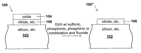
Fig. 2 is a drawing depicting the selective etching of oxide with respect to
surrounding structures using an etching composition in accordance with the
present
invention. In Fig. 2, the structure 100 includes a substrate 102 formed of,
e.g., silicon,
over which is formed a layer of nitride 104. Over the layer of nitride 104 is
formed a
layer of oxide 106, identical to that shown in Fig. 1. If the structure 100 is
subjected to
an etch process using a selective wet etching composition in accordance with
the
present invention, including a sulfonic acid, a phosphonic acid and/or a
phosphinic acid
together with a fluoride, only the layer of oxide 106 is etched away, and
substantially all
of both the layer of nitride 104 and the substrate 102 remain and are not
etched away.
The etching process in Fig. 2 is quite selective, as described herein for the
present
invention. That is, in the product structure 100", the etching process in
accordance
with the present invention selectively removes the layer of oxide 106, while
leaving
substantially all of the layer of nitride 104 and the substrate 102, which are
not
intended to be etched.
Fig. 3 provides exemplary results for an etching composition in accordance
with
the present invention, when it is tested for bath life with time and PSG
loading. The
data in Fig. 3 shows that the etching composition is effective at etching the
oxide,
selective for oxide as compared to nitride and other materials, and efficient
in being
capable of etching a large amount of oxide. In this exemplary embodiment, the
etching
composition comprises 77 wt. % methanesulfonic acid, 3 wt.% hydrogen fluoride
and
the remaining 20 wt. % water. In this exempiary embodiment, the conditions for
the
bath life test are; bath temperature 24 C, 400 g sample, open cup (9:7 aspect
ratio
vessel) with slow stirring and ventilation. Additional PSG is loaded into the
etching
composition every 2 hours over an 8-hour period. Each loading (2 hour
increments) is
calculated to be approximately equivalent to 12.5 wafers (200 mm) processed
with
removal of ca. 16000 A PSG in an 8 gal. immersion bath. The PSG loading is
immediately followed by etch rate tests on PSG, TiN and DCS-nitride at 24 C @
1 min.
As shown in Fig. 3, the PSG etch rate in one exemplary etching composition
slowly
decreases (10-15 %) over an 8-hour period but the PSG/DCS-nitride selectivity
is
maintained. As also shown in Fig. 3, the TiN and polysilicon etch rate remain
low at
less than about 3 A/min and less than about 20 A/min, respectively, over the
entire
bath loading/time test.
6
CA 02608285 2007-11-13
WO 2006/124201 PCT/US2006/015372
Thus, the present invention provides a solution to the problem of selective
etching of oxide with respect to nitride, while maintaining economy and
efficiency.
WET ETCHING COMPOSITIONS
In accordance with one embodiment of the present invention, there is provided
a
wet etching composition including a sulfonic acid, a phosphinic acid, a
phosphonic acid
or a mixture of any two or more such acids, and a fluoride. In one embodiment,
the
etching composition is selective for etching silicon oxynitride, silicon
dioxide and silicate
glasses relative to materials such as silicon nitride, titanium nitride, high-
nitrogen
content silicon oxynitride, metals, silicon and silicides. In one embodiment,
the silicon
comprises one or more of amorphous silicon, polysilicon and monocrystalline
silicon.
In one embodiment, the composition etches PSG at ambient temperature at a
rate ranging from about 1500 to about 15,000 angstrom/minute (A/min), silicon
nitride
at a rate ranging from about 1 to about 20 A/min, titanium nitride at a rate
ranging from
about 0 to about 3 A/min, and polysilicon at a rate ranging from about 0 to
about 20
angstroms/minute. Other materials may have intermediate etch rates, depending
on
the substrate being etched (chemical nature, morphology, deposition method,
etc.) and
the exact etchant composition.
SULFONIC ACIDS
In one embodiment, the etching composition comprises sulfonic acid. In one
embodiment, the etching composition comprises sulfonic acid together with a
phosphinic acid, a phosphonic acid or both.
In one embodiment, the sulfonic acid comprises an alkyl or aryl sulfonic acid.
Alkyl sulfonic acids include, e.g., methane sulfonic acid. Aryl sulfonic acids
include,
e.g., benzene sulfonic acid or toluene sulfonic acid. In one embodiment, the
alkyl
group may be branched or unbranched and may contain from one to about 20
carbon
atoms. In one embodiment, the alkyl group may be substituted or unsubstituted.
In
one embodiment, the aryl group may be alkyl-substituted, i.e., may be an
alkylaryl
group, or may be attached to the sulfonic acid moiety via an alkylene group,
in which
case it may be referred to as an arylalkyl group (and the molecule then would
be
considered an alkyl-substituted sulfonic acid). In one embodiment, the aryl
group may
be substituted with a heteroatom such as those defined in the following as
possible
7
CA 02608285 2007-11-13
WO 2006/124201 PCT/US2006/015372
substituents. In one embodiment, the aryl group may range from six to about 20
carbon atoms, and may be polynuclear.
If the alkyl or aryl sulfonic acid is substituted, the substituents may
comprise
halogens, oxygen, nitrogen (including nitrate, amine, etc.), sulfur (including
thio,
sulfonic, sulfate, sulfoxide, etc.,) or aryl, as defined above. In general,
such
substituents may be suitably selected, together with other atoms, to affect,
adjust
and/or control the activity of the sulfonic acid portion of the molecule.
In one embodiment, the sulfonic acid includes arylalkyl or alkylaryl sulfonic
acids, in which the alkyl substituents may range from C, to about C20 and in
which the
aryl substituents (before substitution) may be phenyl or naphthyl or higher,
or mixtures
of two or more of these, may be suitably used as the acid component. Arylalkyl
sulfonic acids include, e.g., benzyl sulfonic acid. Alkylaryl sulfonic acids
include, e.g.,
toluene sulfonic acid.
In one embodiment, the sulfonic acid comprises methanesulfonic acid,
ethanesulfonic acid, ethane disulfonic acid, propanesulfonic acid,
butanesulfonic acid,
pentanesulfonic acid, hexanesulfonic acid, heptane sulfonic acid,
dodecanesulfonic
acid, benzenesulfonic acid, toluenesulfonic acid, 2-hydroxyethane-sulfonic
acid, alkyl
phenol sulfonic acids, chlorosulfonic acid, fluorosulfonic acid, bromosulfonic
acid,
1-naphthol-4-sulfonic acid, 2-bromoethanesulfonic acid, 2,4,6-
trichlorobenzenesulfonic
acid, phenylmethanesulfonic acid, trifluoromethanesulfonic acid,
perfluorobutyl sulfonic
acid, cetylsulfonic acid, dodecylsulfonic acid, 2-, 3-, or 4-
nitrobenzenesulfonic acid, di-
nitrobenzenesulfonic acid, trinitrobenzenesulfonic acid, benzene-1,4-
disulfonic acid,
methyl-4-nitrobenzenesulfonic acid, methyldichlorobenzene sulfonic acid,
isomers
thereof, corresponding polysulfonic acids or mixtures of any two or more
thereof.
The foregoing are merely exemplary sulfonic acids, and others within the scope
of the general description given above may be suitably selected for use in the
present
invention.
The sulfonic acid is generally present in the etching composition in a
concentration ranging from about 0.1 to about 95 wt.% based on the etching
composition. In one embodiment, the sulfonic acid is present in the etching
composition in a concentration ranging from about 1 to about 50 wt. % based on
the
etching composition. In one embodiment, the sulfonic acid is present in the
etching
8
CA 02608285 2007-11-13
WO 2006/124201 PCT/US2006/015372
composition in a concentration ranging from about 10 to about 90 wt. % based
on the
etching composition. In one embodiment, the sulfonic acid is present in the
etching
composition in a concentration ranging from about 40 to about 80 wt. % based
on the
etching composition. In one embodiment, the sulfonic acid is present in the
etching
composition in a concentration ranging from about 40 to about 50 wt. %, and in
one,
about 45 wt. %, based on the etching composition. In one embodiment, the
sulfonic
acid is present in the etching composition in a concentration ranging from
about 70 to
about 80 wt. %, and in one about 77 wt.%, based on the etching composition.
PHOSPHONIC AND PHOSPHINIC ACIDS
In one embodiment, the etching composition comprises a phosphonic acid,
RPO3H2, which also may be written as RP(O)(OH)2. _Phosphonic acids may also
referred to as organophosphorous acids. In one embodiment, the phosphonic acid
comprises a Cl-Clo branched or unbranched alkyl or C6-C24 aryl or Cl-Clo
branched or
unbranched alkyl-substituted C7-C36 aryl phosphonic acid. In one embodiment,
the
phosphonic acid includes one or more of hydroxyethylidene diphosphonic acid,
nitrilotrimethylene phosphonic acid, methylphosphonic acid and
phenylphosphonic
acid.
In one embodiment, the etching composition comprises a phosphinic acid,
RHPO3H2, which also may be written as RHP(O)(OH)2. In one embodiment, the
phosphinic acid comprises a Cl-Clo branched or unbranched alkyl or C6-C24 aryl
or Cl-
Cjo branched or unbranched alkyl-substituted C7-C36 aryl phosphinic acid.
The acid may include, for example, nitrilotrimethylene phosphonic acid,
hydroxyethylidene diphosphonic acid, phenylphosphonic acid, methylphosphonic
acid,
phenylphosphinic acid, and similar acids based on the phosphonic, phosphinic,
phosphoric, or phosphorous acids. In one embodiment, the phosphonic acid
includes
one or more of hydroxyethylidene diphosphinic acid, nitrilotrimethylene
phosphinic
acid, methylphosphinic acid, and phenylphosphinic acid.
The phosphonic or phosphinic acid is generaiiy present in the etching
composition in a concentration ranging from about 0.1 to about 95 wt.% based
on the
etching composition. In one embodiment, the phosphonic or phosphinic acid is
present
in the etching composition in a concentration ranging from about 1 to about 50
wt. %
based on the etching composition. In one embodiment, the phosphonic or
phosphinic
9
CA 02608285 2007-11-13
WO 2006/124201 PCT/US2006/015372
acid is present in the etching composition in a concentration ranging from
about 10 to
about 90 wt. % based on the etching composition. In one embodiment, the
phosphonic or phosphinic acid is present in the etching composition in a
concentration
ranging from about 40 to about 80 wt. % based on the etching composition. In
one
embodiment, the phosphonic or phosphinic acid is present in the etching
composition
in a concentration ranging from about 40 to about 50 wt. %, and in one, about
45 wt.
%, based on the etching composition. In one embodiment, the phosphonic or
phosphinic acid is present in the etching composition in a concentration
ranging from
about 70 to about 80 wt. %, and in one about 77 wt.%, based on the etching
composition.
In an embodiment in which a mixture or combination of the sulfonic, phosphonic
and/or phosphinic acid is used, the foregoing amounts would be applied to the
total
acid content, and the amount of each of the respective acids in the mixture
may be at
any value within the range for the total acid, with the total applying to the
combination.
FLUORIDES
In one embodiment, the fluoride is hydrogen fluoride, HF. In one embodiment,
the fluoride is a fluoride compound such as NH4F, BF4, PF6, SiF62-,
HF:pyridinium,
quaternary ammonium or phosphonium fluorides or bifluorides, alkyl or aryl
quaternary
ammonium or phosphonium fluorides and mixtures of any two or more thereof.
?0 Bifluorides of the foregoing may also be used.
In one embodiment, the etching composition comprises fluoride in a
concentration from about 0.1 wt.% to about 40 wt.%, based on the etching
composition. In one embodiment, the etching composition comprises fluoride in
a
concentration from about 1 wt. lo to about 40 wt.%, based on the etching
composition.
?5 In one embodiment, the etching composition comprises fluoride in a
concentration from
about 2 wt.% to about 30 wt.%, based on the etching composition. In one
embodiment, the etching composition comprises fluoride in a concentration from
about
2 wt.% to about 20 wt.%, based on the etching composition. In one embodiment,
the
etching composition comprises fluoride in a concentration from about 3 wt.% to
about
30 10 wt.%, and in one embodiment, about 5 wt. %, based on the etching
composition.
CA 02608285 2007-11-13
WO 2006/124201 PCT/US2006/015372
WATER
In one embodiment, the wet etching composition includes less than about 30 wt.
% water, and in another embodiment, from about 5 wt. % to about 30 wt. %
water. In
one embodiment, the wet etching composition includes from about 10 to about 25
wt.
% water, and in another about 15 to about 20 wt. % water, and in another about
17 wt.
% water. The selectivity of the wet etching composition is better when the
water
content is less than about 30 wt. %.
In one embodiment, the wet etching composition is anhydrous. In one
embodiment, the wet etching composition is free of any added water. In this
latter
embodiment, the composition may comprise a small amount of water that is
present as
an impurity or component of one of the materials added to form the wet etching
composition.
NON-AQUEOUS SOLVENT
In one embodiment, the composition further comprises from about 0.1 to about
60 wt.% of a solvent other than water. In one embodiment, the non-aqueous
solvent
comprises sulfolane. In one embodiment, the non-aqueous solvent comprises one
or
more of an alcohol, an alkoxyalcohol, a polyether alcohol. Examples of such
alcohols
and alkoxyalcohols include, for example, methanol, ethanol, propanol,
butoxyethanol,
and butoxyethoxyethanol. Polyether alcohols such as polyoxyalkylenes may also
be
used. In one embodiment, the non-aqueous solvent includes polyethers such as
glyme, diglyme, triglyme, and higher alkyloxyethers. In one embodiment the non-
aqueous solvent comprises a dialkylacetamide, such as dimethylacetamide. In
one
embodiment, the non-aqueous solvent comprises dimethylsulfone,
dimethylsulfoxide,
sulfolane, or a mixture of two or more thereof. Other suitable non-aqueous
solvents
may also be used.
ORGANIC ONIUM FLUORIDES AND COMPOUNDS
In one embodiment, the fluoride may comprise an organic onium fluoride. In
another embodiment, the etching composition may include an organic onium
compound as an additive. Suitable organic onium compounds for the present
invention include organic onium salts and organic onium salts such as
quaternary
ammonium salts, quaternary phosphonium salts, tertiary sulfonium salts,
tertiary
sulfoxonium salts and imidazolium salts. As used herein, disclosure of or
reference to
11
CA 02608285 2007-11-13
WO 2006/124201 PCT/US2006/015372
any onium salt should be understood to include the corresponding salts, such
as
halides, carbonates, formates, sulfates and the like. As will be understood,
such salts
may be prepared from the corresponding hydroxides. In the following discussion
of
onium compounds, the fluorides are generally used as examples; however, it
should be
understood that the other salts noted above may be used instead or in addition
to the
fluorides.
In one embodiment, the onium fluorides may generally be characterized by the
formula I:
A(F)x (I)
wherein A is an onium group and x is an integer equal to the valence of A.
Examples
of onium groups include ammonium groups, phosphonium groups, sulfonium,
sulfoxonium and imidazolium groups. In one embodiment, the onium fluoride
should
be sufficiently soluble in a solution such as water, alcohol or other organic
liquid, or
mixtures thereof to permit a useful wet etch rate.
In one embodiment, the quaternary ammonium fluorides and quaternary
phosphonium fluorides may be characterized by the formula II:
rR2 +
R'-A-R3 F- (II)
R4
wherein A is a nitrogen or phosphorus atom, R', R2, R3 and R4 are each
independently
alkyl groups containing from I to about 20, or 1 to about 10 carbon atoms,
hydroxyalkyl
or alkoxyalkyl groups containing from 2 to about 20, or 2 to about 10 carbon
atoms,
aryl groups or hydroxyaryl groups, or R' and R2 together with A may form a
heterocyclic
group provided that if the heterocyclic group contains a C=A group, R3 is the
second
bond.
The alkyl groups R' to R4 may be linear or branched, and specific examples of
alkyl groups containing from 1 to 20 carbon atoms include methyl, ethyl,
propyl, butyl,
pentyl, hexyl, heptyl, octyl, isooctyl, nonyl, decyl, isodecyl, dodecyl,
tridecyl, isotridecyl,
hexadecyl and octadecyl groups. R1, R2, R3 and R4 also may be hydroxyalkyl
groups
12
CA 02608285 2007-11-13
WO 2006/124201 PCT/US2006/015372
containing from 2 to 5 carbon atoms such as hydroxyethyl and the various
isomers of
hydroxypropyl, hydroxybutyl, hydroxypentyl, etc. In one embodiment, R', R2, R3
and R4
are independently alkyl and/or hydroxyalkyl groups containing 1 to about 4 or
5 carbon
atoms. Specific examples of alkoxyalkyl groups include ethoxyethyl,
butoxymethyl,
butoxybutyl, etc. Examples of various aryl and hydroxyaryl groups include
phenyl,
benzyl, and equivalent groups wherein benzene rings have been substituted with
one
or more hydroxy groups.
In one embodiment, the quaternary onium salts which can be employed in
accordance with the present invention are characterized by the Formula III:
R2 +
R'-A-R3 X-Y (III)
R4 y
wherein A, R1, R2 , R3 and R'' are as defined in Formula II, X- is an anion of
an acid,
e.g., fluoride, and y is a number equal to the valence of X. Examples of
anions of
acids include bicarbonates, halides, nitrates, formates, acetates, sulfates,
carbonates,
phosphates, etc.
- In one embodiment, the quaternary ammonium compounds (fluorides and salts)
which can be treated in accordance with the process of the present invention
may be
represented by Formula IV:
R2 +
R'-N-R3 X-'' (IV)
R~ y
wherein R1, R2 , R3, R4, and y are as defined in Formula II, and X- is a
fluoride anion or
an anion of an acid. In one embodiment, R'- R4 are alkyl and/or hydroxyalkyl
groups
containing from 1 to about 4 or 5 carbon atoms. Specific examples of ammonium
fluorides include tetramethylammonium fluoride (TMAF), tetraethylammonium
fluoride
(TEAF), tetrapropylammonium fluoride, tetrabutylammonium fluoride, tetra-n-
octylam-
monium fluoride, methyltriethylammonium fluoride, diethyldimethylammonium
fluoride,
13
CA 02608285 2007-11-13
WO 2006/124201 PCT/US2006/015372
methyltripropylammonium fluoride, methyltributylammonium fluoride,
cetyltrimethylam-
monium fluoride, trimethylhydroxyethylammonium fluoride, trimethylmethoxyethyl-
ammonium fluoride, dimethyldihydroxyethylammonium fluoride, methyltrihydroxy-
ethylammonium fluoride, phenyltrimethylammonium fluoride,
phenyltriethylammonium
fluoride, benzyltrimethylammonium fluoride, benzyltriethylammonium fluoride,
dimethylpyrolidinium fluoride, dimethylpiperidinium fluoride,
diisopropylimidazolinium
fluoride, N-alkylpyridinium fluoride, etc. In one embodiment, the quaternary
ammonium
fluorides used in accordance with this invention are TMAF and TEAF. The
quaternary
ammonium salts represented by Formula IV may be similar to the above
quaternary
ammonium fluorides except that the fluoride anion is replaced by, for example,
a
sulfate anion, a chloride anion, a carbonate anion, a formate anion, a
phosphate ion,
etc. For example, the salt may be tetramethylammonium chloride,
tetramethylammonium sulfate (y=2), tetramethylammonium bromide, 1-methyl-2-
butyl
imidazolium hexafluorophosphate, n-butyl pyridinium hexafluorophosphate, etc.
Examples of quaternary phosphonium salts representative of Formula III
wherein A=P which can be employed in accordance with the present invention
include
tetramethylphosphonium fluoride, tetraethylphosphonium fluoride,
tetrapropylphosphonium fluoride, tetrabutylphosphonium fluoride, trimethylhy-
droxyethylphosphonium fluoride, dimethyldihydroxyethylphosphonium fluoride,
methyltrihydroxyethylphosphonium fluoride, phenyltrimethylphosphonium
fluoride,
phenyltriethylphosphonium fluoride and benzyltrimethylphosphonium fluoride,
etc, and
the corresponding halides, sulfates, carbonates, phosphates, etc.
In another embodiment, the tertiary sulfonium fluorides and salts which can be
employed in accordance with the present invention may be represented by the
formula
V:
rR2l~
I
R'- S X-'' (V)
1
R3 y
wherein R', R2 and R3, X- and y are as defined in Formula 111.
Examples of the tertiary sulfonium compounds represented by Formula V
include trimethylsulfonium fluoride, triethylsulfonium fluoride,
tripropyisulfonium
14
CA 02608285 2007-11-13
WO 2006/124201 PCT/US2006/015372
fluoride, etc, and the corresponding salts such as the halides, sulfates,
nitrates,
carbonates, etc.
In another embodiment, the tertiary sulfoxonium fluorides and salts which can
be employed in accordance with the present invention may be represented by the
formula VI:
Ra +
I
R1-S=0 X-Y (VI)
1
R3 y
wherein R', R2 and R3, X" and y are as defined in Formula III.
Examples of the tertiary sulfoxonium compounds represented by Formula V
include trimethylsulfoxonium fluoride, triethylsulfoxonium fluoride,
tripropylsulfoxonium
fluoride, etc, and the corresponding salts such as the halides, sulfates,
nitrates,
carbonates, etc.
In another embodiment, the imidazolium fluorides and salts which can be
employed in accordance with the present invention may be represented by the
formula
VII:
R +
I1
F- (Vll)
~
R3
wherein R' and R3 are as defined in Formula II.
Onium fluorides are commercially available. Additionally, onium fluorides can
be prepared from the corresponding onium salts such as the corresponding onium
halides, carbonates, formates, sulfates and the like. Various methods of
preparation
are described in U.S. Patents 4,917,781 (Sharifian et al) and 5,286,354 (Bard
et al)
which are hereby incorporated by reference. There is no particular limit as to
how the
onium fluoride is obtained or prepared.
CA 02608285 2007-11-13
WO 2006/124201 PCT/US2006/015372
In one embodiment, the organic onium fluoride comprises one or more of
tetramethylammonium fluoride, tetraethylammonium fluoride, tetrapropylammonium
fluoride, tetrabutylammonium fluoride, methyltriphenylammonium fluoride,
phenyltrimethylammonium fluoride, benzyltrimethylammonium fluoride,
methyltriethanolammonium fluoride, tetrabutylphosphonium fluoride,
methyltriphenylphosphonium fluoride, trihexyltetradecylphosphonium fluoride,
tributyltetradecylphosphonium fluoride, [(CH3)3NCH2CH(OH)CH2N(CH3)3]2+ [F-]2,
1-
butyl-3-methylimidazolium fluoride, trimethylsulfonium fluoride,
trimethylsulfoxonium
fluoride, trimethyl (2,3-dihydroxypropyl) ammonium fluoride,
[(C6H5)CH2N(CH3)2CH2CH(OH)CH2N(CH3)2CH2CH(OH)CH2N(CH3)2CH2-
CH(OH)CH2N(CH3)2CH2(C6H5)]4+ [F-]4, and [(CH3)3NCH2CH(OH)CH2OH]+ [F], and
hexamethonium difluoride. In one embodiment, the onium fluoride is
benzyltrimethylammonium fluoride.
The concenti-ation of the onium fluoride in the compositions of the present
invention may range up to about 20 wt% of the wet etching composition.
Appropriate
dilutions can be determined by those of skill in the art, based on the
concentration
supplied and the concentration desired to be employed in the wet etching
composition.
In one embodiment, the onium fluoride concentration is in a range from about
0.5 wt%
to about 15 wt%, and in another embodiment, the onium fluoride concentration
is in a
range from about 2 wt% to about 10 wt%, and in another embodiment, the onium
fluoride concentration is in a range from about 3 wt% to about 8 wt%, and in
one
embodiment, the onium fluoride concentration is about 4 wt%, all
concentrations based
on the total weight of the wet etching composition.
AUXILIARY ACIDS
In addition to the sulfonic acid, phosphonic and/or phosphinic acid, in one
embodiment, an auxiliary acid may be added to the etching composition of the
present
invention. Any suitable acid may be used. In one embodiment, the acid is an
organic
acid. In another embodiment, the acid is an inorganic acid. The acid may
include a
mixture or combination of two or more these acids.
In one embodiment, the acid is other than a bi- or higher dentate chelating
agent. In one embodiment, the acid is other than ethylene diamine tetraacetic
acid
16
CA 02608285 2007-11-13
WO 2006/124201 PCT/US2006/015372
(EDTA) or similar chelating agents based on ethylene diamine, diethylene
triamine and
higher multi-amine multi-acetic acid compounds.
Typical examples of the organic acids may include formic acid, acetic acid,
propionic acid, butyric acid, isobutyric acid, valeric acid, ethylmethylacetic
acid,
trimethylacetic acid, glycolic acid, butanetetracarboxylic acid, oxalic acid,
succinic acid,
malonic acid, citric acid, tartaric acid, malic acid, gallic acid, behenic
acid, arachidic
acid, stearic acid, palmitic acid, lauric acid, salicylic acid, benzoic acid,
and
3,5-dihydroxybenzoic acid, or the like. Mixtures of two or more of these acids
may be
used.
Inorganic auxiliary acids may include phosphoric or phosphorous acids and
partial alkyl esters thereof.
Exemplary inorganic and organic acids that may be included in the compositions
include hydrochloric acid, nitric acid, sulfuric acid, sulfurous acid,
hydrobromic acid,
perchloric acid, fluoboric acid, phytic acid, nitrilotriacetic acid, maleic
acid, phthalic
acid, lactic acid, ascorbic acid, gallic acid, sulfoacetic acid, 2-
sulfobenzoic acid,
sulfanilic acid, phenylacetic acid, betaine, crotonic acid, levulinic acid,
pyruvic acid,
trifluoroacetic acid, glycine, cyclohexanecarboxylic acid,
cyclohexanedicarboxylic acid,
cyclopentanedicarboxylic acid, adipic acid, and mixtures or combinations of
two or
more thereof.
In one embodiment, the auxiliary acid may include other, relatively weak,
sulfonic acids such as, for example, N-(2-hydroxyethyl)-N'-(2-ethane sulfonic
acid)
(HEPES), 3-(N-morpholino) propane sulfonic acid (MOPS) and piperazine-N,N'-
bis(2-
ethane sulfonic acid) (PIPES).
The concentration of the auxiliary acid in the compositions of the present
invention may range from 0.1 wt% to about 10 wt% of the etching composition.
Appropriate dilutions can be determined by those of skill in the art, based on
the
concentration supplied and the concentration desired to be employed in the wet
etching composition. In one embodiment, the auxiliary acid concentration is in
a range
from about 0.2 wt% to about 5 wt%, and in another embodiment, the auxiliary
acid
concentration is in a range from about 0.5 wt% to about 4 wt%, and in another
embodiment, the auxiliary acid concentration is in a range from about 1 wt% to
about 3
wt%, and in one embodiment, the auxiliary acid concentration is about 2 wt lo,
all
17
CA 02608285 2007-11-13
WO 2006/124201 PCT/US2006/015372
concentrations based on the total weight of the wet etching composition, and
are in
addition to the sulfonic acid component. The concentration of the auxiiiary
acid may be
adjusted based on factors such as the strength (or pKa), solubility and
complexing
power of the acid.
In one embodiment, the composition is substantially free of added
hydroxylamine, nitrate, persulfate or any combination of two or more thereof.
WET ETCHING COMPOSITION pH
The pH of the wet etching composition in accordance with the present invention
may be a pH in the range from about -1 to about 3, and in one embodiment, a pH
in
the range from about 0 to about 2, and in another embodiment, a pH of about 1,
and in
one embodiment, the pH is about 1.5. In one embodiment, the composition has a
pH
less than about 2. The pH can be adjusted as needed by manipulating sulfonic
acid
and/or auxiliary acid selection, acid concentration, selection of fluoride and
fluoride
concentration and by addition of suitable buffers, if required, as will be
understood by
those of skill in the art. As will be recognized, reference to "pH" in the wet
etching
compositions applies to the hydrogen ion concentration as if these
compositions had a
much higher water content in which the acid is capable of fully dissociating.
In order to
measure the pH by, e.g., a pH meter, it may be necessary to dilute the wet
etching
composition by a factor of 10 or 100. In one embodiment, the "pH" referred to
herein
relates to the pH of the same acid dissolved in water at the same
concentration as in
the present invention. Thus, it wouid be assumed that the acid is fully
dissociated in
the wet etching compositions of the present invention, for purposes of
referring to the
pH of the composition.
PHOTORESISTS
The present invention may be used with a variety of different photoresist
materials, including but not limited to, Novolacs, methacrylates, acrylates,
styrenes,
sulfones and isoprenes. Exemplary photoresist materials include positive
photoresists,
such as those that include a Novolac resin, a diazonaphthaquinone, and a
solvent
(e.g., n-butyl alcohol or xylene), and negative photoresist materials, such as
those that
include a cyclized synthetic rubber resin, bis-arylazide, and an aromatic
solvent. In one
embodiment, suitable photoresists include negative photoresists, such as for
example,
MacDermid Aquamer CFI or MI, du Pont Riston 9000, or du Pont Riston 4700, or
18
CA 02608285 2007-11-13
WO 2006/124201 PCT/US2006/015372
Shipley UV5 and TOK DP019. Positive photoresists include AZ3312, AZ3330,
Shipley
1.2L and Shipley 1.8M. Negative photoresists include nLOF 2020 and SU8.
Examples
of additional suitable resists include the AZ 5218, AZ 1370, AZ 1375, or AZ
P4400,
from Hoechst Celanese; CAMP 6, from OCG; DX 46, from Hoechst Celanese; XP
8843, from Shipley; and JSR/NFR-016-D2, from JSR, Japan. Suitable photoresists
are
described in U.S. Pat. Nos. 4,692,398; 4,835,086; 4,863,827 and 4,892,801.
Suitable
photoresists may be purchased commercially as AZ-4620, from Clariant
Corporation of
Somerville, N.J. Other suitable photoresists include solutions of
polymethylmethacrylate (PMMA), such as a liquid photoresist available as 496 k
PMMA, from OLIN HUNT/OCG, West Paterson, N.J. 07424, comprising
polymethylmethacrylate with molecular weight of 496,000 dissolved in
chlorobenzene
(9 wt %); (meth)acrylic copolymers such as P(MMA-MAA) (poly methyl
methacrylate-methacrylic acid); PMMA/P(MMA-MAA) polymethylmethacrylate/(poly
methyl methacrylate-methacrylic acid). Any suitable photoresist, whether
existing or
yet-to-be-developed, is contemplated, regardless of whether such comprises a
positive
or negative type photoresist.
METHODS OF SELECTIVE OXIDE ETCHING
In accordance with another embodiment of the present invention, there is
provided a process of selectively etching oxide relative to nitride, metal,
silicon or
silicide, comprising:
providing a substrate comprising oxide and one or more of nitride, metal,
silicon
or silicide in which the oxide is to be etched;
applying to the substrate for a time sufficient to remove a desired quantity
of
oxide from the substrate an etching composition comprising:
a sulfonic acid and
a fluoride; and
removing the etching composition,
wherein the oxide is removed selective to the one or more of nitride, metal,
silicon or silicide.
In one embodiment, the methods used in carrying out the process of the present
invention are substantially similar or the same as wet etching methods known
in the
art, except for the use of the wet etching composition in accordance with the
present
19
CA 02608285 2007-11-13
WO 2006/124201 PCT/US2006/015372
invention. Thus, in one embodiment, all that is needed to carry out the method
of the
present invention is to substitute the wet etching composition of the present
invention
into a conventional wet etching process.
In one embodiment, the etching composition is applied at a temperature in the
range from about 15 C to about 60 C. Additional details on temperatures are
given
below.
In one embodiment, the etching composition is removed by washing with a
rinse composition comprising water and/or a solvent.
In one embodiment, the oxide is removed at a rate greater than about 1500
angstroms/minute at a temperature of about 20 C. Additional details on etch
rates are
given below.
The following describes exemplary conditions for carrying out embodiments of
this method. Additional details and modifications can be determined by those
of skill in
the art.
PROCESSING TIME
The time needed for carrying out a method of selectively wet etching a silicon
oxide in accordance with an embodiment of the present invention may be
suitably
selected based on factors known to those of skill in the art, including the
identity of the
silicon oxide to be etched, the thickness of the silicon oxide to be etched,
the method
by which the silicon oxide was deposited (which may affect properties such as
hardness, porosity and texture of the silicon oxide), concentrations of
sulfonic acid,
fluoride, other ingredients, temperature and rate of stirring or mixing of the
wet etching
composition, volume of the wet etching composition relative to the quantity
and/or size
of wafers or parts to be treated, and similar factors known to affect etch
rates in
conventional silicon oxide etching methods. In one embodiment, the time of
exposure
of the wet etching composition to the silicon oxide ranges from about 1 minute
to about
60 minutes, and in another embodiment, the time ranges from about 2 minutes to
about 40 minutes, and in another embodiment the time ranges from about 5
minutes to
about 20 minutes, and in yet another embodiment, the time ranges from about 7
to
about 15 minutes. In one embodiment, the time ranges from about 30 seconds to
about 4 minutes.
CA 02608285 2007-11-13
WO 2006/124201 PCT/US2006/015372
PROCESSING TEMPERATURES
The bath or composition temperature for carrying out a method of selectively
wet etching a silicon oxide in accordance with an embodiment of the present
invention
may be suitably selected based on factors known to those of skill in the art,
including
the identity of the silicon oxide to be etched, the thickness of the silicon
oxide to be
etched, the method by which the silicon oxide was deposited (which may affect
properties such as hardness, porosity and texture of the silicon oxide),
concentrations
of sulfonic acid, fluoride, other ingredients, rate of stirring or mixing of
the wet etching
composition, volume of the wet etching composition relative to the quantity
and/or size
of wafers or parts to be treated, the time allotted for the etching, and
similar factors
known to affect etch rates in conventional silicon oxide etching methods. In
one
embodiment, the bath or composition temperature of the wet etching composition
for
wet etching the silicon oxide ranges from about 15 C to about 60 C, and in
another
embodiment, the bath or composition temperature ranges from about 20 C to
about
45 C, and in another embodiment the bath or composition temperature ranges
from
about 25 C to about 40 C, and in yet another embodiment, the bath or
composition
temperature ranges from about 25 C to about 35 C.
ETCH RATES
Etch rates may be suitably selected by those of skill in the art based on
factors
known, such as time, temperature, identity of the sulfonic acid, of the
fluoride and of
the silicon oxide to be etched, and on the selectivity attained for the
specific materials
surrounding the silicon oxide to be etched, and other factors known or easily
determined by persons of skill in the art.
As noted, the intent of the present invention is to etch oxides, e.g., silicon
oxides
such as those defined above, selectively with respect to materials which
commonly
surround or exist in adjacent or nearby structures, and which could be etched
by the
same etching composition in the absence of such selectivity. Thus, the etching
composition should exhibit a high etch rate of such oxides, while exhibiting a
comparatively low etch rate of such materials that are not intended to be
etched, such
as nitrides, high-nitrogen content silicon oxynitride, metals, silicon,
silicides and
photoresist materials.
21
CA 02608285 2007-11-13
WO 2006/124201 PCT/US2006/015372
In one embodiment, the etching composition has an etching rate of silicon
nitride of less than about 20 angstroms/minute. In one embodiment, , the
etching
composition has an etching rate of silicon nitride of less than about 10
angstroms/minute. In one embodiment, , the etching composition has an etching
rate
of silicon nitride of less than about 5 angstroms/minute.
In one embodiment, the etching composition has an etching rate of high
nitrogen content silicon oxynitride of less than about 15 angstroms/minute. In
one
embodiment, the etching composition has an etching rate of high nitrogen
content
silicon oxynitride of less than about 10 angstroms/minute. In one embodiment,
the
etching composition has an etching rate of high nitrogen content silicon
oxynitride of
less than about 5 angstroms/minute. High nitrogen content silicon oxynitride
is defined
to contain less than about 5 atomic weight percent oxygen. High oxygen content
silicon oxynitride is defined to contain less than about 5 atomic weight
percent nitrogen.
In one embodiment, the etching composition has an etching rate of titanium
nitride of less than about 3 angstroms/minute.
In one embodiment, the etching composition has an etching rate of polysilicon
of
less than about 20 angstroms/minute. In one embodiment, the etching
composition
has an etching rate of polysilicon of less than about 10 angstroms/minute. In
one
embodiment, the etching composition has an etching rate of polysilicon of less
than
about 5 angstroms/minute.
In one embodiment, the etching composition has an etching rate of 6%
phosphorus-doped oxide (PSG) from about 1500 angstrom/min to about 15,000
angstrom/min. In one embodiment, the etching composition has an etching rate
of
boron-phosphorus-doped oxide (BPSG) from about 1500 angstrom/min. to about
15,000 angstrom/min. In one embodiment, the etching composition has an etching
rate of 6% boron-doped oxide (BSG) from about 1500 angstrom/min. to about
15,000
angstrom/min. In one embodiment, the etching composition has an etching rate
of
high oxygen content silicon oxynitride from about 1500 angstrom/min. to about
15,000 angstrom/min. Silicon oxynitride is generally referred to as SiON, and
includes SiOXNY and SiOXNyHZ, in which x, y and z are appropriate
stoichiometric
values for a substantially balanced compound. As noted above, high oxygen
content
silicon oxynitride contains less than about 5 atomic weight percent nitrogen.
1n one
22
CA 02608285 2007-11-13
WO 2006/124201 PCT/US2006/015372
embodiment, the etching composition has an etching rate of disilane-based CVD
deposited silicon dioxide from about 1500 angstrom/min. to about 15,000
angstrom/min. In one embodiment, the etching composition has an etching rate
of
thermally formed silicon dioxide from about 1500 angstrom/min. to about 15,000
angstrom/min. In one embodiment, the etching composition has an etching rate
of
TEOS-source spin-on silicon dioxide from about 1500 angstrom/min. to about
15,000
angstrom/min. In one embodiment, the etching composition has an etching rate
of
TEOS-source CVD deposited silicon dioxide from about 1500 angstrom/min. to
about
15,000 angstrom/min.
As will be recognized, the etch rates for all of the relevant materials may
vary
to some extent, based on factors such as differences in morphology or
material, the
method by which the material was formed or deposited, whether the material was
densified, whether the material was damaged or otherwise treated to increase
its
etchability, and other relevant treatments that may have an effect on the
actual,
observed etch rate. In the present invention, it is the relative etch rates,
and
selectivities, that are of primary importance.
SELECTIVITY
In one embodiment, the etching composition has a selectivity for etching CVD
oxide, thermal oxide, TEOS oxide, PSG, BPSG, BSG, high oxygen content silicon
oxynitride and combinations of any two or more thereof relative to silicon
nitride,
titanium nitride, high nitrogen content siiicon oxynitride, metal,
polysilicon,
monocrystalline silicon and metal silicides ranging from about 15,000:1 to
about
200:1. In one embodiment, the etching composition has a selectivity for
etching PSG
relative to CVD dichloro-silane silicon nitride ranging from about 200:1 to
about
800:1, at about 23 C. In one embodiment, the etching composition has a
selectivity
for etching PSG relative to CVD dichloro-silane silicon nitride ranging from
about
250:1 to about 700:1, at about 23 C. In one embodiment, the etching
composition
has a selectivity for etching PSG relative to CVD dichloro-silane silicon
nitride ranging
from about 300:1 to about 600:1, at about 23 C. These relative etch rates and
selectivities relate to these specific materials, and corresponding
selectivities may be
observed for other materials or materials applied or deposited by other
methods
and/or having other morphologies.
23
CA 02608285 2007-11-13
WO 2006/124201 PCT/US2006/015372
In one embodiment, the composition has a selectivity for etching HPCVD
oxide, APCVD oxide, thermal oxide, BPTEOS oxide, TEOS oxide, PSG, BPSG, BSG,
high oxygen content silicon oxynitride, SiOC and combinations of any two or
more
thereof relative to one or more of silicon nitride, high nitrogen content
silicon
oxynitride, titanium nitride, metal, polysilicon, monocrystalline silicon and
metal
silicides ranging from about 15,000:1 to about 200:1.
EXEMPLARY EXPERIMENTAL PROCEDURE:
The following is an exemplary process for carrying out an embodiment of the
present invention, and is provided for exemplary, non-limiting purposes.
PSG Project Wafers
10000-15000 A BPSG on silicon
200-300 A TiN on 1000 A SiO2on silicon
200-300 A Polysilicon on 1000 A Si02 on silicon
10000-13000 A PSG on silicon
1000-1500 A HCD-nitride on silicon
1000-1500 A DCS-nitride on silicon
In one embodiment, operating temperature for the PSG etchant chemistries is
C. The DCS, HCD nitrides, PSG, TiN, SOD (spin-on-dielectric; e.g., SOG) and
Polysilicon wafers are cleaved into 1" x 1" square pieces. The pieces are
submerged
20 into the etchant solutions at temperatures of 22-26 C. The wafer pieces are
processed for 1 minute after which they are rinsed with DI water and blown dry
with
nitrogen. The film thicknesses before and after processing are determined by
reflectometry for PSG and DCS-nitride using a NANOSPEC 210 and by resistance
for TiN using a Tencor RS35c. The films are also examined by optical
microscopy to
25 assess uniformity of etch.
The conditions for the bath life test are: bath temperature of 24 C, 400 g
sample, open cup (9:7 aspect ratio vessel) with slow stirring and ventilation.
PSG
loading of the bath life sample is accomplished by processing wafer pieces
with
known surface area in 400 g of etchant to remove about 8500 A of PSG (1 min
process) every 2 hours for 8 hours total. After each loading, etch tests on
PSG, TiN,
Polysilicon, and DCS nitride are performed. The PSG loading factor in Fig. 1
in ppm
(using a PSG density of 2.3 g/cm3) represents the cumulative amount of PSG
etched.
24
CA 02608285 2007-11-13
WO 2006/124201 PCT/US2006/015372
Assuming 16000 A PSG is removed over the entire surface area of a 200 mm wafer
in an 8 gallon immersion bath, each 2 hours in the exemplary bath loading test
(in
ppm of PSG removed) is equivalent to 12.5 (200 mm) wafers processed.
RESULTS:
A comparison of three PSG etchant formulations is given in Table 1. The
results for PSG DCS-nitride, polysilicon, and TiN etch rate for SFE-1 126
versus bath
age and loading are presented in Table 2. PSG, DCS-nitride, polysilicon, and
TiN
etch rate versus temperature is provided for SFE-1 126 in Table 3.
Table 1: Comparison of SFE-1044, SFE-1069 and SFE-1126
Sample T( C) PSG DCS-Nitride HCD- TiN Poly Si PSG/DCS-
/Time (A/min) (A/min) Nitride (AJmin) (11/min) Nitride
(min.) (A/min)
SFE-1 044 23/1 8279 14.5 57 < 0.1 8.3 571
SFE-1069 23/1 14394 18 67.5 < 0.1 8.3 800
SFE-1126 23/1 7586 11 43 < 0.1 11 690
SFE-1 044 Composition: 33 %, Sulfolane, 45 % Methanesulfonic Acid, 5 % HF, 17
% Water
SFE-1069 Composition: 80 % Methanesulfonic Acid, 5% HF, 15 /o Water
SFE-1126 Composition: 77 % Methanesulfonic Acid, 3% HF, 20 % Water
Table 2: Processed in SFE-1126 at 24 C @ 1 min
Sample PSG DCS-Nitride TiN Polysilicon PSG/DCS- PSG Loading
(Almin) (Almin) (A/min) (A/min) Nitride ppm*
Initial Pour = 0 hrs 8446 12.3 0.23 7 687 0
Time = 2 hrs 8383 13.0 0.06 14.5 645 51
Time = 4 hrs 7744 11.7 0 14 662 100
Time = 6 hrs 8045 14.0 0.54 10 575 154
Time = 8 hrs 6991 11.3 0.77 11.7 619 207
* assumes PSG density of 2.3 g/cm3
Table 3: SFE-1126 etch rates versus T( C)
T( C) PSG (Almin) DCS-Nitride TiN Poly Si PSGIDCS-
(A/min) (Almin) (A/min) Nitride
19.5 6202 11 < 0.1 0.3 564
21 7040 13.3 < 0.1 5.5 529
24 7586 12.3 < 0.1 11 617
26 8185 13.3 < 0.1 6.5 615
CA 02608285 2007-11-13
WO 2006/124201 PCT/US2006/015372
DISCUSSION OF EXAMPLES
The primary focus of these examples is on selectively etching PSG relative to
DCS-nitride, TiN and Polysilicon (Table 1) and to a bath life loading and time
study
monitoring etch rates on PSG, DCS-nitride, TiN and polysilicon for one of
these
formulations, namely, SFE-1 126 (Table 2). A graph of PSG, DCS-nitride, TiN
and
Polysilicon etch rate and selectivity versus bath loading and age for SFE-1
126 is
provided in Fig. 1. Etch rate change with temperature for SFE-1126 is shown in
Table
3.
Three different PSG etchants are described with PSG etch rates ranging from
7000-14000 A/min and selectivities to DCS-nitride of 500-800:1. All etchants
have low
etch rates on TiN and polysilicon. In general, PSG etch rate can be varied in
the
range of 4000-15000 A/min with selectivity to DCS-nitride of 300-800 with
slight
modifications in etch chemistry between SFE-1044, 1069 and 1126.
In one embodiment, SFE-1 126 is well suited for single wafer processing, where
a 1-2 min process per wafer is desirable. The SFE-1 126 etch rate varies by
only 1145
A/min over a 5 C range (19-26 C). This corresponds to < 300 A/min per degree C
for
PSG or < 4 % etch rate change at 24 C 0.5 C. SFE-1 126 is designed for
operation
at or below 25 C to obtain the best bath life and etch characteristics (i.e.
selectivity).
Throughout the foregoing specification and the following claims, the numerical
limits of the ranges and ratios, including concentrations, pH, wavelengths and
other
ranges, may be combined. That is, for example, where ranges of 1 to 10 and 2
to 5
are disclosed, although not specifically stated, this disclosure should be
understood to
also include the range from 2 to 10 and from 1 to 5, as well as intervening
integral
values as range limits.
While the invention has been explained in relation to certain of its exemplary
embodiments, it is to be understood that various modifications thereof will
become
apparent to those skilled in the art upon reading the specification.
Therefore, it is to
be understood that the invention disclosed herein is intended to cover such
modifica-
tions as fall within the scope of the appended claims.
26