Note: Descriptions are shown in the official language in which they were submitted.
CA 02608323 2007-11-13
WO 2006/124576 PCT/US2006/018409
INTEGRATED CIRCUIT WITH SIGNAL BUS
FORMED BY CELL ABUTMENT OF LOGIC CELLS
CROSS-REFERENCE TO RELATED APPLICATIONS
[0001] This application claims the benefit of U.S. Provisional Application
Serial Number
60/680,888 titled "Integrated Circuit Layout with Sleep Transistors," filed
May 13, 2005, which
is hereby incorporated by reference.
BACKGROUND
1. Field of the Invention
[0002] The present invention relates generally to integrated circuits, and
more
particularly to an integrated circuit with a signal bus formed by cell
abutment of logic cells.
2. Description of Related Art
[0003] Many designs for integrated circuits use standard cell libraries. The
standard cell
libraries provide the building blocks of logic cells to allow designers to go
quickly from circuit
design to semiconductor chip fabrication and test. Metal interconnects are
employed to connect
signals to each of the logic cells in an integrated circuit.
[0004] One example using metal interconnects to distribute a signal to logic
cells is a
sleep signal for sleep transistors. Sleep transistors have been added to the
functionality of logic
CA 02608323 2007-11-13
WO 2006/124576 PCT/US2006/018409
cells available in standard cell libraries. The sleep transistors are
controlled by the sleep signal
and provide the ability to control power consumption in the individual logic
cells.
[0005] A sleep signal may be used by sleep transistors to switch the
individual logic
cells into sleep mode. In sleep mode, the power consumption of the individual
logic cells is
reduced. Sleep transistors may be particularly important in devices using
integrated circuits in
which lower power consumption is an important feature as, for example, in cell
phones or mobile
computers.
[0006] Because space in an integrated circuit is limited, the space occupied
by the sleep
transistors and related circuitry needs to be minimized. The addition of the
sleep transistors to
standard cells has caused the height of the logic cell to increase. The added
sleep transistors also
require additional routing resources, which are limited due to the preexisting
design of the
integrated circuit layout. A separate sleep pin is also required to receive
the sleep signal in each
individual logic cell with a sleep transistor. Thus, the addition of sleep
transistors to standard
cells has resulted in increased complexity that may result in layout
congestion and blockages.
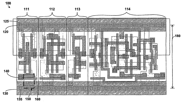
[0007] FIG. 1 is an illustration of integrated circuit layout 100 employing
sleep circuitry
in the prior art. Integrated circuit layout 100 includes four logic cells 111,
112, 113 and 114.
Integrated circuit layout 100 also includes VDD power bus 120, VDD tap 125,
VSS power bus
130, VSS tap 135, sleep pin 140, sleep transistor 150, and gate 160.
Integrated circuit layout 100
has height 180.
[0008] Logic cell 111 draws its power from VDD power bus 120, and from VSS
power
bus 130 as controlled by sleep transistor 150. Logic cell 111 comprises sleep
transistor 150 and
gate 160 coupled to sleep pin 140. Sleep transistor 150 may be configured to
switch VSS power
2
CA 02608323 2007-11-13
WO 2006/124576 PCT/US2006/018409
to the logic cell 111 on and off in response to a sleep signal received at
sleep pin 140, and
thereby to control power consumption in logic cell 111.
[0009] Each logic cell 111, 112, 113, and 114 contains sleep circuitry
comprising a sleep
transistor substantially similar to sleep transistor 150. Sleep pin 140
requires a metal layer and a
second metal interconnect drop using a via to connect the sleep pins from each
logic cell 111,
112, 113, and 114, thus requiring two routing resources, the metal layer and
the metal
interconnect. In addition, logic cells may be defined in increments of tracks,
such that when
routing metal interconnects the number of tracks is a whole number. In FIG. 1,
the addition of
sleep circuitry requires an additional track for routing the metal
interconnect, resulting in an
increase in height 180 and area of the logic cells 111, 112, 113, and 114 by
approximately 11%.
[0010] In another example, Multi-Threshold Complementary Metal Oxide
Semiconductor (MTCMOS) integrated circuits use one or more sleep transistors
located in one
region of an integrated circuit. A virtual ground from a plurality of logic
cells is routed to the
drains of the sleep transistors, thus controlling the power for the plurality
of logic cells.
MTCMOS suffers, however, from the phenomena of electro-migration. Since the
virtual ground
carries a pulsed direct current, electro-migration limits the long-term
reliability of the integrated
circuit. In addition, the use of virtual ground typically requires another
track of height in the cell.
[0011] Thus, adding sleep circuitry comprising sleep transistors to the
individual logic
cells in the standard cell libraries has several disadvantages. The
disadvantages include
increasing the height of the logic cells, the addition of a metal layer, the
congestion and resulting
difficulty of routing to the sleep pin in each logic cell, and the problem of
electro-niigration in
the MTCMOS example.
3
CA 02608323 2007-11-13
WO 2006/124576 PCT/US2006/018409
SUMMARY OF THE INVENTION
[0012] The invention addresses the problems discussed above by providing an
integrated
circuit with a signal bus formed by the cell abutment of logic cells. The
integrated circuit
comprises at least two logic cells. The signal bus is formed by the cell
abutment of the at least
two logic cells. The signal bus is configured to receive a signal and
distribute the signal to each
of the at least two logic cells.
[0013] The signal bus may be formed from a first semiconductor layer
comprising a
polycrystalline silicon layer. The signal bus may comprise a sleep bus that
distributes a sleep
signal to each of the at least two logic cells. A sleep pin may be coupled to
the sleep bus and
may receive the sleep signal. Sleep circuitry may be coupled to the logic
cells and may receive
the sleep signal from the sleep bus and may control power consumption in the
logic cells based
on the sleep signal. The sleep circuitry may comprise one or more sleep
transistors. The drain of
the sleep transistors may be formed from a second semiconductor layer. The
sleep transistors
may comprise NMOS transistors or PMOS transistors.
[0014] Various embodiments of the invention include a method comprising
receiving a
signal using a signal bus formed by cell abutment of at least two logic cells,
and distributing the
signal to each of the at least two logic cells.
4
CA 02608323 2007-11-13
WO 2006/124576 PCT/US2006/018409
BRIEF DESCRIPTION OF THE DRAWINGS
[0015] FIG. 1 is an illustration of an integrated circuit layout employing
sleep circuitry in
the prior art;
[0016] FIG. 2 is an illustration of an integrated circuit layout employing
sleep circuitry in
an exemplary implementation of the invention;
[0017] FIG. 3 is an illustration of an integrated circuit layout for an
inverter logic cell in
an exemplary implementation of the invention;
[0018] FIG. 4 is an illustration of an integrated circuit layout for an
inverted input two-
input NAND gate logic cell in an exemplary implementation of the invention;
[0019] FIG. 5 is an illustration of an integrated circuit layout for a non-
sleep inverter
logic cell that is bypassed by the sleep bus in an exemplary implementation of
the invention;
[0020] FIG. 6 is an illustration of an integrated circuit layout for a flip-
flop logic cell in
an exemplary implementation of the invention; and
[0021] FIG. 7 is an illustration of an integrated circuit layout employing a
shared sleep
transistor in an exemplary implementation of the invention.
CA 02608323 2007-11-13
WO 2006/124576 PCT/US2006/018409
DETAILED DESCRIPTION OF THE INVENTION
[0022] The embodiments discussed herein are illustrative of one example of the
present
invention. As these embodiments of the present invention are described with
reference to
illustrations, various modifications or adaptations of the methods and/or
specific structures
described may become apparent to those skilled in the art. All such
modifications, adaptations,
or variations that rely upon the teachings of the present invention, and
through which these
teachings have advanced the art, are considered to be within the scope of the
present invention.
Hence, these descriptions and drawings should not be considered in a limiting
sense, as it is
understood that the present invention is in no way limited to only the
embodiments illustrated.
[0023] The integrated circuit comprises at least two logic cells and a signal
bus formed
by the cell abutment of the at least two logic cells. The signal bus is
configured to receive a
signal and to distribute the signal to each of the at least two logic cells.
One advantage is that the
signal bus may provide an overall reduction in the area of the logic cells. A
second advantage is
the uncomplicated routing of the signal bus during the integrated circuit
design process. A third
advantage is that the performance of the logic cells using a signal bus formed
by cell abutment is
not degraded.
[0024] A signal bus formed by cell abutment comprises circuitry formed by
coupling of
adjacent logic cells at the edge of the logic cells. When logic cells are
fabricated, these abutment
regions may be joined by a single semiconductor layer, such as a
polycrystalline silicon layer,
that spans across a plurality of logic cells. A signal bus thus formed may
distribute a signal to
each logic cell over which the polycrystalline silicon layer passes.
[0025] Using cell abutment of the logic cells, various signals may be
distributed through
the signal bus to the logic cells. One example of the signal bus is a sleep
bus. FIGs. 2 through 7
6
CA 02608323 2007-11-13
WO 2006/124576 PCT/US2006/018409
and the related descriptions disclose distributing a sleep signal using a
sleep bus. However, one
skilled in the art should understand that other embodiments include
distributing other signals
using a signal bus.
[0026] FIG. 2 is an illustration of an integrated circuit layout 200 employing
sleep
circuitry in an exemplary implementation of the invention. The integrated
circuit layout 200 is
fabricated on a semiconductor substrate and is formed from multiple layers of
doped regions and
layers, metal layers, and polycrystalline silicon layers. The integrated
circuit layout 200 includes
logic cells 211, 212, and 213, cell 214, VDD power bus 220, VDD tap 225,
antenna diodes 227,
VSS power bus 230, VSS tap 235, sleep pin 240, sleep transistors 250, sleep
bus 260, n+
diffusion 265 and abutting region 270. The integrated circuit layout 200 has
height 280.
[0027] FIG. 2 depicts only three logic cells 211, 212, and 213 for the sake of
simplicity.
However, in other embodiments, integrated circuits may include a plurality of
logic cells. Logic
cell 211 is an example of the layout of logic cells in the integrated circuit
layout 200. Other logic
cells, such as logic cells 212 and 213, may have similar layouts and
configurations as logic cell
211.
[0028] Logic cells are standard cells designed primarily to perform logic
functions such
as boolean operations. Logic cells may also perform a sequence of logic
functions. Logic cells
211, 212, and 213 are configured to perform logic functions including, but not
limited to,
inverters, NOR gates, NAND gates, flip-flops, and adders. Logic cells 211,
212, and 213 are
each coupled to VDD power bus 220 at the top portion of each logic cell. VDD
tap 225 is also
coupled to VDD power bus 220.
[0029] In various embodiments, sleep transistor 250 comprises a portion of an
underlying
n+ diffusion 265 overlaid by a portion of sleep bus 260. Sleep bus 260 is
formed from a
7
CA 02608323 2007-11-13
WO 2006/124576 PCT/US2006/018409
polycrystalline silicon layer. The combination of a portion of the underlying
n+ diffusion 265
overlaid by a portion of sleep bus 260 forms a NMOS transistor, such as sleep
transistor 250.
The gate of sleep transistor 250 is formed by a portion of sleep bus 260
comprising the
polycrystalline silicon layer. Logic cell 212 includes sleep transistor 251,
which performs the
same function as sleep transistor 250 in logic cell 211.
[0030] Sleep circuitry is any circuitry coupled to the logic cells and
configured to receive
a sleep signal from the sleep bus and to control the power consumption in the
logic cells based
on the sleep signal. Sleep circuitry in logic cell 212, for example, comprises
sleep transistor 251
formed from a portion of underlying n+ diffusion 266 and a portion of sleep
bus 260. Because of
the limited space available and the kind of logic implemented in each of the
logic cells 211, 212,
and 213, the layout of the sleep circuitry varies within each logic cell.
[0031] In other embodiments, sleep circuitry may be implemented using PMOS
transistors (not shown) by overlaying a polycrystalline silicon layer with a
portion of an
underlying p+ diffusion region (not shown). In these embodiments, sleep
circuitry comprising
PMOS transistors may be located adjacent to VDD power bus 220. FIGs. 2 through
7 and the
related descriptions disclose sleep circuitry comprising of one or more NMOS
transistors. FIG.
2, for example, discusses sleep circuitry with one NMOS transistor in each
logic cell. In another
embodiment discussed in FIG. 6 below, sleep circuitry with multiple NMOS
transistors in a
single logic cell is disclosed. In another embodiment discussed in FIG. 7
below, sleep circuitry
with a single NMOS transistor shared among three logic cells is disclosed.
However, one skilled
in the art should understand that various embodiments include sleep circuitry
comprising one or
more PMOS transistors, and sleep circuitry comprising both NMOS and PMOS
transistors.
8
CA 02608323 2007-11-13
WO 2006/124576 PCT/US2006/018409
[0032] Logic cells 211 and 212 are coupled to VSS power bus 230 through sleep
circuitry comprising sleep transistors 250 and 251, thereby enabling sleep
transistors 250 and
251 to control the power to logic cells 211 and 212. Sleep transistors 250 and
251 control the
power to logic cells 211 and 212 in response to a sleep signal from sleep bus
260. Sleep pin 240
is coupled to sleep bus 260, and sleep pin 240 provides an external connection
(not shown) for
the sleep signal.
[0033] A sleep bus is any structure that is configured to distribute a sleep
signal to the
sleep circuitry in each of the logic cells. Sleep bus 260, for example, forms
a continuous
semiconductor layer that spans across each of the logic cells 211, 212, 213,
and cell 214.
Because the logic cells 211, 212, and 213 are adjacent, sleep bus 260 is
coupled to each bf the
logic cells 211, 212, and 213 by cell abutment. FIG. 2 depicts abutting region
270 that couples
sleep bus 260 between logic cell 211 and logic cell 212.
[0034] One advantage of the integrated circuit layout 200 is the reduced
height and area
of the logic cells. Sleep bus 260 and sleep transistors 250 and 251, for
example, control the
power to logic cells 211 and 212. Using sleep bus 260, a single VSS tap 235
can be placed in
cell 214, instead of in every logic cell. In addition, instances of VDD tap
225 are removed from
logic cells 211, 212, and 213, and a single VDD tap 225 is placed in cell 214.
Thus, more space
is available to implement logic functions in logic cells 211, 212, and 213, or
optionally the
overall size of the logic cells and thus the size of the integrated circuit
may be reduced. In one
embodiment, the height 280 and area of logic cells 211, 212 and 213 are
approximately 11 Io less
than the prior art of FIG. 1.
[0035] A second advantage of the integrated circuit layout 200 is the
uncomplicated
routing of the sleep bus during the integrated circuit design process. Sleep
bus 260 may be
9
CA 02608323 2007-11-13
WO 2006/124576 PCT/US2006/018409
routed like a power bus or a ground bus. In addition, using sleep bus 260 and
locating VDD tap
.225 and VSS tap 235 in cell 214 may utilize nine tracks to implement logic
cells 211, 212, and
213. The height 280 of logic cells, such as logic cell 211, 212, and 213 may
be characterized by
the whole number of tracks required, depending on the need to route metal
interconnects. In the
prior art shown in FIG. 1, the addition of sleep circuitry requires a total of
ten tracks because of
the need to route a metal interconnect to couple to each instance of sleep pin
140, thus adding to
the complexity of the layout. In one embodiment, the logic cells with sleep
circuitry are reduced
in height and area by approximately 11%. The integrated circuit layout 200
optionally includes
antenna diodes 227 in cell 214 for electrostatic discharge protection during
the semiconductor
fabrication process.
[0036] A third advantage is that the performance of the logic cells with sleep
circuitry is
not degraded. Logic cells 211, 212, and 213 have a performance substantially
similar or better
than the prior art of FIG. 1 because more space is available for logic cells
211, 212, and 213 in
the integrated circuit layout 200. In some embodiments, the NMOS transistors
may be located
lower in logic cells 211, 212, and 213 than the PMOS transistors. As the
result of these factors,
the delay times through logic cells 211, 212, and 213 are substantially
similar or better than the
prior art of FIG. 1.
[0037] Using cell abutment, a single polycrystalline silicon layer can be
configured to
distribute other signals to each of the logic cells 211, 212, and 213. In this
embodiment, a signal
bus distributes signals to a plurality of logic cells 211, 212, and 213.
[0038] In the embodiment shown in FIG. 2, VDD tap 225 for VDD power bus 220 is
not
located in each logic cell 211, 212, and 213. Instead, VDD tap 225 is located
in cell 214. VDD
power bus 220 couples to a supply of power through VDD tap 225. Sleep bus 260
also couples
CA 02608323 2007-11-13
WO 2006/124576 PCT/US2006/018409
to sleep pin 240 in cell 214. In addition, VSS tap 235 is located in cel1214.
Cel1214 is
optionally placed every 25 microns or other spacing as required by the
integrated circuit foundry.
[0039] FIG. 3 is an illustration of an integrated circuit layout for an
inverter logic cell
300, in an exemplary implementation of the invention. The inverter logic cell
300 comprises
VDD power bus 220, VSS power bus 230, sleep transistor 350, sleep bus 260, n+
diffusion 365,
left extended portion 371 of sleep bus 260, right extended portion 372 of
sleep bus 260, and n-
we11375. The inverter logic cell 300 has height 380.
[0040] Left extended portion 371 of sleep bus 360 and a right extended portion
372 of
sleep bus 360 illustrate the cell abutment region. When at least two logic
cells, such as any of
logic cells 211, 212, 213, or inverter logic cel1300 are located adjacent to
each other, sleep bus
260 spans across the logic cells. Sleep bus 260 thereby couples the at least
two logic cells by cell
abutment, and distributes the sleep signal to other sleep transistors, as
discussed above. In this
embodiment, the height 380 and area of the inverter logic cell 300 is
approximately 11% less
than the prior art of FIG. 1 because only nine tracks are required.
[0041] FIG. 4 is an illustration of an integrated circuit layout for inverted
input two-input
NAND gate logic ce11400, in an exemplary implementation of the invention.
Inverted input
two-input NAND gate logic ce11400 includes VDD power bus 220, VSS power bus
230, sleep
transistor 450, sleep bus 260, n-we11475, left extended portion 471 of sleep
bus 260, and right
extended portion 472 of sleep bus 260. Inverted input two-input NAND gate
logic cell 400 has
height 480.
[0042] FIG. 4 depicts sleep bus 260 comprising a left extended portion 471 of
sleep bus
260 and right extended portion 472 of sleep bus 260 to illustrate the cell
abutment region. In this
embodiment, the height 480 is approximately 11% less than the prior art of
FIG. 1 because only
11
CA 02608323 2007-11-13
WO 2006/124576 PCT/US2006/018409
nine tracks are required. Thus, the area of the inverted input two-input NAND
gate 400 reduced
by approximately 11%, as compared with the prior art of FIG. 1.
[0043] FIG. 5 is an illustration of an integrated circuit layout for a non-
sleep inverter
logic cell 500. Non-sleep inverter logic cell 500 is bypassed by sleep bus 260
in an exemplary
implementation of the invention. In various embodiments, integrated circuits
may require logic
cells which require continuous power. Non-sleep inverter logic cell 500 is one
such example.
Non-sleep inverter logic cell 500 does not employ a sleep transistor.
[0044] FIG. 5 depicts a single non-sleep inverter logic cell 500 for
simplicity. Non-sleep
inverter logic cell 500 comprises VDD power bus 220, VSS power bus 230, sleep
bus 260, left
extended portion 571 of sleep bus 260, right extended portion 572 of sleep bus
260, n-well 575,
and VSS power coupling 590. The non-sleep inverter logic ce11500 has height
580. Height 580
may be approximately equal to height 380 of the inverter logic cel1300.
[0045] FIG. 5 depicts sleep bus 260 comprising a left extended portion 571 and
a right
extended portion 572 to illustrate the cell abutment region. As contrasted to
the inverter logic
cell 300, shown in FIG. 3, the embodiment of the non-sleep inverter logic
cel1500 does not
contain a sleep transistor, such as sleep transistor 350.
[0046] Non-sleep inverter logic cell 500 does not contain an n+ diffusion
underlying
sleep bus 260, such as n+ diffusion 365, and thus no sleep transistor is
formed. Sleep bus 260
does not couple to VSS power coupling 590. Sleep bus 260 passes over, or
bypasses, VSS
power coupling 590. In this embodiment, sleep bus 260 distributes the sleep
signal across the
non-sleep inverter logic cell 500 to adjacent logic cells, without receiving
the sleep signal within
the non-sleep inverter logic cell 500.
12
CA 02608323 2007-11-13
WO 2006/124576 PCT/US2006/018409
[0047] FIG. 6 is an illustration of an integrated circuit layout for flip-flop
logic cell 600,
in an exemplary implementation of the invention. Flip-flop logic cell 600
includes VDD power
bus 620, VSS power bus 630, sleep transistors 650, 651, and 652, sleep bus
660, n-well 675, left
extended portion 671 of sleep bus 660, right extended portion 672 of sleep bus
660, and n+
diffusion 665, 666, and 667. FIG. 6 illustrates one embodiment of the
invention in which more
than one sleep transistor is employed within a single logic cell. For example,
sleep transistors
650, 651, and 652 are all contained in flip-flop logic cell 600. Flip-flop
logic cell 600 has height
680.
[0048] FIG. 6 depicts sleep bus 660 comprising a left extended portion 671 of
sleep bus
660 and right extended portion 672 of sleep bus 660 to illustrate the cell
abutment region. In this
embodiment, the height 680 is approximately 11% less than the prior art of
FIG. 1.
[0049] FIG. 7 is an illustration of an integrated circuit layout 700 employing
a shared
sleep transistor in an exemplary implementation of the invention. The
integrated circuit layout
700 is fabricated on a semiconductor substrate and is formed from multiple
layers of doped
regions and layers, metal layers, and polycrystalline silicon layers.
Integrated circuit layout 700
includes logic cells 711, 712, and 713, cell 714, VDD power bus 720, VDD tap
725, antenna
diodes 727, VSS power bus 730, VSS tap 735, sleep pin 740, shared sleep
transistor 750, sleep
bus 760, extended drain 765, abutting region 770, abutting region 771, and n-
well 775.
Integrated circuit layout 700 has height 780. In other embodiments using cell
abutment, a single
polycrystalline silicon layer can be configured to distribute signals to each
of the logic cells 711,
712, and 713. In these embodiment, a signal bus distributes signals to a
plurality of logic cells
711, 712, and 713.
13
CA 02608323 2007-11-13
WO 2006/124576 PCT/US2006/018409
[0050] FIG. 7 depicts only three logic cells 711, 712, and 713 for the sake of
simplicity.
However, in other embodiments, integrated circuits may include a plurality of
logic cells. Logic
cell 711 is an example of the layout of logic cells in the integrated circuit
layout 700. Other logic
cells, such as logic cells 712 and 713, have similar layouts and
configurations.
[0051] Logic cells 711, 712, and 713 are configured to perform logic functions
including,
but not limited to, inverters, NOR gates, NAND gates, flip-flops, and adders.
Logic cells 711,
712, and 713 are each coupled to VDD power bus 720 at the top portion of each
logic cell. VDD
tap 725 is coupled to VDD power bus 720.
[0052] Logic cells 711, 712, and 713 are coupled to VSS power bus 730 through
extended drain 765 and shared sleep transistor 750, thereby enabling shared
sleep transistor 750
to control power to logic cells 711, 712, and 713. Shared sleep transistor 750
controls the power
to logic cells 711, 712, and 713 in response to a sleep signal from sleep bus
760.
[0053] In various embodiments, shared sleep transistor 750 comprises a portion
of an
underlying n+ diffusion forming extended drain 765. Extended drain 765 spans
across at least
two logic cells and is overlaid by a portion of sleep bus 760. Sleep bus 760
is formed from a
polycrystalline silicon layer. The combination of extended drain 765 overlaid
by sleep bus 760
forms a single NMOS transistor, such as shared sleep transistor 750, which is
shared by logic
cells 711, 712 and 713. The gate of shared sleep transistor 750 is formed by a
portion of sleep
bus 760 comprising the polycrystalline silicon layer.
[0054] In other embodiments, a shared sleep transistor, similar to shared
sleep transistor
750, may be implemented using PMOS transistors (not shown) by overlaying a
polycrystalline
silicon layer with a portion of an underlying p+ diffusion region (not shown).
In these
embodiments, the shared sleep transistor may be located adjacent to VDD power
bus 620.
14
CA 02608323 2007-11-13
WO 2006/124576 PCT/US2006/018409
[0055] Sleep bus 760 is formed by cell abutment because logic cells 711, 712,
and 713
are adjacent. In the same fashion, extended drain 765 is formed by cell
abutment. FIG. 7 depicts
abutting regions 770 and 771 between logic cell 711 and logic cell 712, and
abutting regions 772
and 773 between logic cell 712 and logic cell 713. Thus, for example, sleep
bus 760 spans
across logic cells 711 and 712 and is coupled at abutting region 771. In the
same way, extended
drain 765 spans across logic cells 711 and 712 and is coupled at abutting
region 770. Because of
the limited space available and the kind of logic circuitry implemented in
each of the logic cells
711, 712, and 713, the layout of extended drain 765 varies within each logic
cell 711, 712, and
713. Sleep pin 740 is coupled to sleep bus 760, and sleep pin 740 provides an
external
connection (not shown) for the sleep signal.
[0056] Cell 714 couples VDD power bus 720 to a supply of power through VDD tap
725.
VSS tap 735 couples power to VSS bus 730. Cell 714 also couples sleep bus 760
to sleep pin
740. In the embodiment shown in FIG. 7, VDD tap 725 for VDD power bus 720 is
not located
in each logic cell 711, 712, and 713. Instead, a single VDD tap 725 is located
in cell 714. In
addition, VSS tap 735 is located in cell 714. The integrated circuit layout
700 optionally
includes antenna diodes 727 for electrostatic discharge protection during the
semiconductor
fabrication process. Cell 714 is optionally placed every 25 microns or other
spacing as required
by the integrated circuit foundry.
[0057] By removing instances of VDD tap 725 and VSS tap 735 from logic cells
711,
712, and 713, and placing a single VDD tap 725 and a single VSS tap 735 in
cell 714, more
space is provided to implement logic functions in logic cells 711, 712, and
713. In this
embodiment, the height 780 and area of logic cells 711, 712 and 713 is
approximately 11% less
than the prior art.
CA 02608323 2007-11-13
WO 2006/124576 PCT/US2006/018409
[0058] The combination of sleep bus 760 and extended drain 765 forming shared
sleep
transistor 750 has the advantage of requiring a smaller area on the integrated
circuit than do the
sleep transistors in the prior art. A single shared sleep transistor 760 also
improves the delay
time through each logic cell 711, 712, and 713. In addition, the integrated
circuit layout 700
advantageously does not employ a virtual ground bus. A virtual ground bus may
cause
performance degradation due to resistance, and can suffer from the phenomena
of electro-
migration, which limits the long term reliability of integrated circuits.
[0059] The above description is illustrative and not restrictive. Many
variations of the
invention will become apparent to those of skill in the art upon review of
this disclosure. The
scope of the invention should, therefore, be determined not with reference to
the above
description, but instead should be determined with reference to the appended
claims along with
their full scope of equivalents.
16