Note: Descriptions are shown in the official language in which they were submitted.
CA 02608528 2007-11-14
WO 2006/138441
PCT/US2006/023277
BOOST DEVICES AND METHODS OF USING THEM
FIELD OF THE TECHNOLOGY
[1]
Certain examples disclosed herein relate generally to boost devices, for
example,
boost devices configured to provide radio frequencies. More particularly,
certain examples
relate to boost devices that may be used to provide additional energy to an
atomization
source, such as a flame or a plasma.
BACKGROUND
o [2]
Atomization sources, such as flames, may be used for a variety of
applications, such
as welding, chemical analysis and the like. In= some instances, flames used in
chemical
analyses are not hot enough to vaporize the entire liquid sample that is
injected into the
flame. In addition, introduction of a liquid sample may result in zonal
temperatures that
may provide mixed results.
[3] Another approach to atomization is to use a plasma source. Plasmas have
been used
in many technological areas including chemical analysis. Plasmas are
electrically
conducting gaseous mixtures containing large concentrations of cations and
electrons. The
temperature of a plasma may be as high as around 6,000-10,000 Kelvin,
depending on the
region of the plasma, whereas the temperature of a flame is often about 1400-
1900 Kelvin,
depending on the region of the flame. Due to the higher temperatures of the
plasma, more
rapid vaporization, atomization and/or ionization of chemical species may be
achieved.
[4] Use of plasmas may have several drawbacks in certain applications.
Viewing
optical emissions from chemical species in the plasma may be hindered by a
high
background signal from the plasma. Also, in some circumstances, plasma
generation may
require high total flow rates of argon (e.g., about 11-17 L/min) to create the
plasma,
including a flow rate of about 5-15 L/min of argon to isolate the plasma
thermally. In
addition, injection of aqueous samples into a plasma may result in a decrease
in plasma
temperature due to evaporation of solvent, i.e., a decrease in temperature due
to desolvation.
This temperature reduction may reduce the efficiency of atomization and
ionization of
chemical species in some contexts.
[5] Higher powers have been used in plasmas to attempt to lower the
detection limits for
certain species, such as hard-to-ionize species like arsenic, cadmium,
selenium and lead, but
increasing the power also results in an increase in the background signal from
the plasma.
1
CA 02608528 2007-11-14
WO 2006/138441
PCT/US2006/023277
[6] Certain aspects and examples of the present technology alleviate some
of the above
concerns with previous atomization sources. For example, a boost device is
shown here as
a way to assist other atomization sources, such as flames, plasmas, arcs and
sparks. Certain
of these embodiments may enhance atomization efficiency, ionization
efficiency, decrease
background noise and/or increase emission signals from atomized and ionized
species.
SUMMARY
[7] In accordance with a first aspect, a boost device is disclosed. As used
throughout
this disclosure, the term "boost device" refers to a device that is configured
to provide
additional energy to another device, or region of that device, such as, for
example, an
atomization chamber, desolvation chamber, excitation chamber, etc. In certain
examples, a
radio frequency (RF) boost device may be configured to provide additional
energy, e.g., in
the form of radio frequency energy, to an atomization source, such as a flame,
plasma, arc,
spark or combinations thereof. Such additional energy may be used to assist in
desolvation,
atomization and/or ionization of species introduced into the atomization
source, may be
used to excite atoms or ions, may be used to extend optical path length, may
be used to
improve detection limits, may be used to increase sample size loading or may
be used for
many additional uses where it may be desirable or advantageous to provide
additional
energy to an atomization source. Other uses of the boost devices disclosed
herein will be
recognized by the person of ordinary skill in the art, given the benefit of
this disclosure, and
exemplary additional uses of the boost devices in chemical analysis, welding,
sputtering,
vapor deposition, chemical synthesis and treatment of radioactive waste are
provided below
to illustrate some of the features and uses of certain illustrative boost
devices disclosed
herein.
[8] In accordance with other aspects, an atomization device is provided. In
certain
examples, the atomization device may include a chamber configured with an
atomization
source and at least one boost device configured to provide radio frequency
energy to the
chamber. The atomization source may be a device that may atomize and/or ionize
species
including but not limited to flames, plasmas, arcs, sparks, etc. The boost
device may be
configured to provide additional energy to a suitable region or regions of the
chamber such
that species present in the chamber may be atomized, ionized and/or excited.
Suitable
devices and components for designing or assembling the atomization source and
the boost
device will be readily selected by the person of ordinary skill in the art,
given the benefit of
this disclosure, and exemplary devices and components are discussed below.
2
CA 02608528 2007-11-14
WO 2006/138441
PCT/US2006/023277
[9] In accordance with yet other aspects, another example of an atomization
device is
disclosed. In certain examples, the atomization devices include a first
chamber and a
second chamber. The first chamber includes an atomization source. The
atomization
source may be a device that may atomize and/or ionize species including but
not limited to
flames, plasmas, arcs, sparks, etc. The second chamber may include at least
one boost
device configured to provide radio frequency energy to the second chamber to
provide
additional energy to excite any atoms or ions that enter into the second
chamber. In this
embodiment, the first and second chambers may be in fluid communication such
that
species that are atomized or ionized in the first chamber may enter into the
second chamber.
Po Suitable examples of configurations for providing fluid
communication between the first
chamber and the second chamber are discussed below, and additional
configurations may be
selected by the person of ordinary skill in the art, given the benefit of this
disclosure.
[10] In accordance with other aspects, a device for optical emission
spectroscopy
("OES") is disclosed. In certain examples, the OES device may include a
chamber that
includes an atomization source and at least one= boost device configured to
provide radio
frequency energy to the chamber. In other examples, the OES device may include
a first
chamber that includes an atomization source and a second chamber that may
include a boost
device configured to provide radio frequencies to the second chamber. The
atomization
source may be a flame, plasma, arc, spark or other suitable devices that may
atomize and/or
ionize chemical species introduced into the first chamber. The OES device may
further
include a light detector configured to detect the= amount of light and/or the
wavelength of
light emitted by species that are atomized and/or ionized using the OES
device. Depending
on the configuration of the OES device, the OES device may be used to detect
atomic
emission, fluorescence, phosphorescence and other light emissions. The OES
device may
further include suitable circuitry, algorithms and software. It will be within
the ability of
the person of ordinary skill in the art, given the benefit of this disclosure,
to design suitable
OES devices for an intended use. In certain examples, the OES device may
include two or
more plasma sources for atomization, ionization and/or detection of species.
[11] In accordance with still other aspects, a device for absorption
spectroscopy ("AS") is
disclosed. In certain examples, the AS device may include a chamber that
includes an
atomization source and at least one boost device configured to provide radio
frequency
energy to the chamber. In other examples, the AS device may include at least a
first
chamber that includes an atomization source and a second chamber in fluid
communication
with the first chamber. The second chamber may include at least one boost
device
3
CA 02608528 2007-11-14
WO 2006/138441
PCT/US2006/023277
configured to provide radio frequency energy to the second chamber. The
atomization
source may be a flame, plasma, arc, spark or other suitable sources that may
atomize and/or
ionize chemical species. The AS device may further include a light source
configured to
provide one or more wavelengths of light and a light detector configured to
detect the
amount of light absorbed by the species present in one or more of the
chambers. The AS
device may further include suitable circuitry, algorithms and software of the
type known in
the art for such devices.
[12] In accordance with yet other aspects, a device for mass spectroscopy
("MS") is
disclosed. In certain examples, the MS device may include an atomization
device coupled
or hyphenated to a mass analyzer, a mass detector or a mass spectrometer. In
some
examples, the MS device includes an atomization device with a chamber that
includes an
atomization source and at least one boost device configured to provide radio
frequency
energy to the chamber. In other examples, the MS device includes a first
chamber that
includes an atomization source and a second chamber in fluid communication
with the first
chamber. The second chamber may include at least one boost device configured
to provide
radio frequency energy to the second chamber. The atomization source may be a
flame,
plasma, arc, spark or other suitable sources that may atomize and/or ionize
chemical
species. In some examples, the MS device may be configured such that the
chamber, or
first and second chambers, may be coupled or hyphenated to a mass analyzer, a
mass
detector or mass spectrometer such that species that exit the chamber, or
first and second
chambers, may enter into the mass analyzer, mass detector or mass spectrometer
for
detection. In other examples, the MS device may be configured such that
species first enter
into the mass analyzer, mass detector or mass spectrometer and then enter into
the chamber,
or first and second chambers, for detection using optical emission,
absorption, fluorescence
or other spectroscopic or analytical techniques. It will be within the ability
of the person of
ordinary skill in the art, given the benefit of this disclosure, to select
suitable devices and
methods to couple mass analyzers, mass detectors or mass spectrometers with
the
atomization devices disclosed herein to perform mass spectroscopy.
[13] In accordance with yet other aspects, a device for infrared spectroscopy
("IRS") is
disclosed. In certain examples, the IRS device may include an atomization
device coupled
or hyphenated to an infrared detector or infrared spectrometer. In some
examples, the IRS
device may include an atomization device with a chamber that includes an
atomization
source and at least one boost device configured to provide radio frequency
energy to the
chamber. In other examples, the IRS device may include a first chamber that
includes an
4
CA 02608528 2007-11-14
WO 2006/138441
PCT/US2006/023277
atomization source and a second chamber in fluid communication with the first
chamber.
The second chamber may also include at least one boost device configured to
provide radio
frequency energy to the second chamber. The atomization source may be a flame,
plasma,
arc, spark or other suitable sources that may atomize and/or ionize chemical
species. In
some exainples, the IRS device may be configured such that the chamber, or
first and
second chambers, may be coupled or hyphenated to an infrared detector or
infrared
spectrometer such that species that exit the chamber, or the first and second
chambers, may
enter into the infrared detector for detection. In other examples, the IRS
device may be
configured such that species first enter into the infrared detector or
infrared spectrometer
and then enter into the chamber, or first and second chambers, for detection
using optical
emission, absorption, fluorescence or other suitable spectroscopic or
analytical techniques.
[14] In accordance with additional aspects, a device for fluorescence
spectroscopy
("FLS") is disclosed. In certain examples, the FLS device may include an
atomization
device coupled or hyphenated to a fluorescence detector or fluorimeter. In
some examples,
the FLS device may include an atomization device with a chamber that includes
an
atomization source and at least one boost device configured to provide radio
frequency
energy to the chamber. In other examples, the FLS device may include a first
chamber that
includes an atomization source and a second chamber in fluid communication
with the first
chamber. The second chamber may include at least one boost device configured
to supply
radio frequency energy to the second chamber. The atomization source may be a
flame,
plasma, arc, spark or other suitable sources that may atomize and/or ionize
chemical
species. In some examples, the FLS device may be configured such that the
chamber, or
first and second chambers, of the atomization device may be coupled or
hyphenated to a
fluorescence detector or fluorimeter such that species that exit the chamber,
or first and
second chambers, may enter into the fluorescence detector for detection. In
other examples,
the FLS device may be configured such that species first enter into the
fluorescence detector
or fluorimeter and then enter into the chamber, or first and second chambers,
of the
atomization device for detection using optical emission, absorption,
fluorescence or other
suitable spectroscopic or analytical techniques.
[15] In accordance with further aspects, a device for phosphorescence
spectroscopy
("PHS") is disclosed. In certain examples, the PHS device may include an
atomization
device coupled or hyphenated to a phosphorescence detector or phosphorimeter.
In some
examples, the PHS device may include an atomization device with a chamber that
includes
an atomization source and at least one boost device configured to provide
radio frequency
5
CA 02608528 2007-11-14
WO 2006/138441
PCT/US2006/023277
energy to the chamber. In other examples, the PHS device may include a chamber
that
includes an atomization source and a second chamber in fluid communication
with the first
chamber. The second chamber may include at least one boost device configured
to provide
radio frequency energy to the chamber. The atomization source may be a flame,
plasma,
arc, spark or other suitable sources that may atomize and/or ionize chemical
species. In
some examples, the PHS device may be configured such that the chamber, or
first and
second chambers, of the atomization device may be coupled or hyphenated to a
phosphorescence detector or phosphorimeter such that species that exit the
chamber, or first
and second chambers, may enter into the phosphorescence detector for
detection. In other
examples, the PHS device may be configured such that species first enter into
the
phosphorescence detector or phosphorimeter and then enter into the chamber, or
first and
second chambers, of the atomization device for detection using optical
emission, absorption,
fluorescence or other suitable spectroscopic or analytical techniques.
[16] In accordance with other embodiments, a device for Raman spectroscopy
("RAS") is
disclosed. In certain examples, the RAS device may include an atomization
device coupled
or hyphenated to a Raman detector or Raman spectrometer. In some examples, the
RAS
device may include an atomization device with a chamber that includes an
atomization
source and at least one boost device configured to provide radio frequency
energy to the
chamber. In other examples, the RAS device may include a first chamber that
includes an
atomization source and a second chamber in fluid communication with the first
chamber.
The second chamber may include a boost device configured to supply radio
frequency
energy to the second chamber. The atomization source may be a flame, plasma,
arc, spark
or other suitable sources that may atomize and/or ionize chemical species. In
some
examples, the RAS device may be configured such that the chamber, or first and
second
chambers, of the atomization device may be coupled or hyphenated to a Raman
detector or
Raman spectrometer such that species that exit the chamber, or first and
second chambers,
may enter into the Raman detector or spectrometer for detection. In other
examples, the
RAS device may be configured such that species first enter into the Raman
detector or
Raman spectrometer and then enter into the chamber, or first and second
chambers, of the
atomization device for detection using optical emission, absorption,
fluorescence or other
suitable spectroscopic or analytical techniques.
[17] In accordance with other aspects, a device for X-ray spectroscopy ("XRS")
is
disclosed. In certain examples, the XRS device may include an atomization
device coupled
or hyphenated to an X-ray detector or an X-ray spectrometer. In some examples,
the XRS
6
CA 02608528 2007-11-14
WO 2006/138441
PCT/US2006/023277
device may include an atomization device with a chamber that includes an
atomization
source and at least one boost device configured to provide radio frequency
energy to the
chamber. In other examples, the XRS device may include a first chamber that
includes an
atomization source and a second chamber in fluid communication with the first
chamber.
The second chamber may include a boost device configured to supply radio
frequency
energy to the second chamber. The atomization source may be a flame, plasma,
arc, spark
or other suitable sources that may atomize and/or ionize chemical species. In
some
examples, the XRS device may be configured such that the chamber, or first and
second
chambers, of the atomization device may be coupled or hyphenated to an X-ray
detector or
an X-ray spectrometer such that species that exit the chamber, or first and
second chamber,
may enter into the X-ray detector or spectrometer for detection. In other
examples, the XRS
device may be configured such that species first enter into the X-ray detector
or an X-ray
spectrometer and then enter into the chamber, or first and second chambers, of
the
atomization device for detection using optical emission, absorption,
fluorescence or other
suitable spectroscopic or analytical techniques.
[18] In accordance with additional aspects, a device for gas chromatography
("GC") is
disclosed. In certain examples, the GC device may include an atomization
device coupled
or hyphenated to a gas chromatograph. In some examples, the GC device may
include an
atomization device with a chamber that includes an atomization source and at
least one
boost device configured to provide radio frequency energy to the chamber. In
other
examples, the GC device may include a first chamber that includes an
atomization source
and a second chamber in fluid communication with the first chamber. The second
chamber
may include at least one boost device configured to provide radio frequency
energy to the
second chamber. The atomization source may be a flame, plasma, arc, spark or
other
suitable sources that may atomize and/or ionize chemical species. In some
examples, the
GC device may be configured such that the chamber, or first and second
chambers, of the
atomization device may be coupled or hyphenated to a gas chromatograph such
that species
that exit the chamber, or first and second chambers, may enter into the gas
chromatograph
for separation and/or detection. In other examples, the GC device may be
configured such
that species first enter into the gas chromatograph and then enter into the
chamber, or first
and second chambers, of the atomization device for detection using optical
emission,
absorption, fluorescence or other suitable spectroscopic or analytical
techniques.
[19] In accordance with other aspects, a device for liquid chromatography
("LC") is
disclosed. In certain examples, the LC device may include an atomization
device coupled
7
CA 02608528 2007-11-14
WO 2006/138441
PCT/US2006/023277
or hyphenated to a liquid chromatograph. In some examples, the LC device may
include an
atomization device with a chamber that includes an atomization source and at
least one
boost device conf igured to provide radio frequency energy to the chamber. In
other
examples, the LC device may include a first chamber that includes an
atomization source
and a second chamber in fluid communication with the first chamber. The second
chamber
may include at least one boost device configured to provide radio frequency
energy to the
second chamber. The atomization source may be a flame, plasma, arc, spark or
other
suitable sources that may atomize and/or ionize chemical species. In some
examples, the
LC device may be configured such that the chamber, or first and second
chambers, of the
io atomization device may be coupled or hyphenated to a liquid
chromatograph such that
species that exit the chamber, or first and second chambers, may enter into
the liquid
chromatograph for separation and/or detection. In other examples, the LC
device may be
configured such that species first enter into the liquid chromatograph and
then enter into the
chamber, or first and second chambers, of the atomization device for detection
using optical
emission, absorption, fluorescence or other suitable spectroscopic or
analytical techniques.
[20] In accordance with still other aspects, a device for nuclear magnetic
resonance
("NMR") is disclosed. In certain examples, the NMR device may include an
atomization
device coupled or hyphenated to a nuclear magnetic resonance detector or a
nuclear
magnetic resonance spectrometer. In some examples, the NMR device includes an
atomization device with a chamber that includes an atomization source and at
least one
boost device conf igured to provide radio frequency energy to the chamber. In
other
examples, the NMR device may include a first chamber that includes an
atomization source
and a second chamber in fluid communication with the first chamber. The second
chamber
may include at least one boost device configured to provide radio frequency
energy to the
second chamber. The atomization source may be a flame, plasma, arc, spark or
other
suitable sources that may atomize and/or ionize chemical species. In some
examples, the
NMR device may be configured such that the chamber, or first and second
chambers, of the
atomization device may be coupled or hyphenated to a nuclear magnetic
resonance detector
or a nuclear magnetic resonance spectrometer such that species that exit the
chamber, or
first and second chambers, may enter into the nuclear magnetic resonance
detector or
nuclear magnetic resonance spectrometer for detection. In other examples, the
nuclear
magnetic resonance detector or nuclear magnetic resonance spectrometer may be
configured
such that species first enter into the nuclear magnetic resonance detector or
nuclear
magnetic resonance spectrometer and then enter into the chamber, or first and
second
8
CA 02608528 2007-11-14
WO 2006/138441
PCT/US2006/023277
chambers, of the atomization device for detection using optical emission,
absorption,
fluorescence or other spectroscopic or analytical techniques. It will be
within the ability of
the person of ordinary skill in the art, given the benefit of this disclosure,
to select suitable
devices and methods to couple nuclear magnetic resonance detectors or nuclear
magnetic
resonance spectrometers with the atomization devices disclosed here to perform
nuclear
magnetic resonance spectroscopy.
[21] In accordance with additional aspects, a device for electron spin
resonance ("ESR")
is provided. In certain examples, the ESR device may include an atomization
device
coupled or hyphenated to an electron spin resonance detector or an electron
spin resonance
spectrometer. In some examples, the ESR device may include an atomization
device with a
chamber that includes an atomization source and at least one boost device
configured to
provide radio frequency energy to the chamber. In other examples, the ESR
device may
include a first chamber that includes an atomization source and a second
chamber in fluid
communication with the first chamber. The second chamber may include at least
one boost
device configured to provide radio frequency energy to the second chamber. The
atomization source may be a flame, plasma, arc, spark or other suitable
sources that may
atomize and/or ionize chemical species. In some examples, the ESR device may
be
configured such that the chamber, or first and second chambers, of the
atomization device
may be coupled or hyphenated to an electron spin resonance detector or an
electron spin
resonance spectrometer such that species that exit the chamber, or first
chamber and second
chambers, may enter into the electron spin resonance detector or the electron
spin resonance
spectrometer for detection. In other examples, the electron spin resonance
detector or the
electron spin resonance spectrometer may be configured such that species first
enter into the
electron spin resonance detector or the electron spin resonance spectrometer
and then enter
into the chamber, or first and second chambers, of the atomization device for
detection
using optical emission, absorption, fluorescence or other spectroscopic or
analytical
techniques.
[22] In accordance with other aspects, a welding device is disclosed. The
welding device
may include an electrode, a nozzle tip and at least one boost device
surrounding at least
some portion of the electrode and/or the nozzle tip and configured to provide
radio
frequencies. Welding devices which include a boost device may be used in sui
table
welding applications, for example, in tungsten inert gas (TIG) welding, plasma
arc welding
(PAW), submerged arc welding (SAW), laser welding, and high frequency welding.
Exemplary configurations implementing the boost devices disclosed here in
combination
9
CA 02608528 2007-11-14
WO 2006/138441
PCT/US2006/023277
with torches for welding are discussed below and other suitable configurations
will be
readily selected by the person of ordinary skill in the art, given the benefit
of this disclosure.
[23] In accordance with additional aspects, a plasma cutter is provided. In
certain
examples, the plasma cutter may include a chamber or channel that includes an
electrode.
The chamber or channel in this example may be configured such that a cutting
gas may flow
through the chamber and may be in fluid communication with the electrode and
such that a
shielding gas may flow around the cutting gas and the electrode to minimize
interferences
such as oxidation of the cutting surface. The plasma cutter of this example
may further
include at least one boost device configured to increase ionization of the
cutting gas and/or
increase the temperature of the cutting gas. Suitable cutting gases may be
readily selected
by the person of ordinary skill in the art, given the benefit of this
disclosure, and exemplary
cutting gases include, for example, argon, hydrogen, nitrogen, oxygen and
mixtures thereof.
[24] In accordance with yet additional aspects, a vapor deposition device is
disclosed. In
certain examples, the vapor deposition device may include a material source, a
reaction
chamber, an energy source with at least one boost device, a vacuum system and
an exhaust
system. The vapor deposition device may be configured to deposit material onto
a sample
or substrate.
[25] In accordance with yet other aspects, a sputtering device is disclosed.
In certain
examples, the sputtering device may include a target and a heat source
including at least one
boost device. The heat source may be configured to cause ejection of atoms and
ions from
the target. The ejected atoms and ions may be deposited, for example, on a
sample or
substrate.
[26] In accordance with other aspects, a device for molecular beam epitaxy is
disclosed.
In certain examples, the device may include a growth chamber configured to
receive a
sample, at least one material source configured to provide atoms and ions to
the growth
chamber, and at least one boost device configured to provide radio frequency
energy to the
at least one material source. The molecular beam epitaxy device may be used,
for example,
to deposit materials onto a sample or substrate.
[27] In accordance with further aspects, a chemical reaction chamber is
disclosed. In
certain examples, the chemical reaction chamber includes a reaction chamber
with an
atomization source and at least one boost device configured to provide radio
frequency
energy to the chemical reaction chamber. The reaction chamber may further
include an
inlet for introducing reactants and/or catalysts into the reaction chamber.
The reaction
CA 02608528 2007-11-14
WO 2006/138441
PCT/US2006/023277
chamber may be used, for example, to control or promote reactions between
products or to
favor one or more products produced from the reactants.
[28] In accordance with yet other aspects, a device for treatment of
radioactive waste is
disclosed. In certain examples, the device includes a chamber configured to
receive
radioactive waste, an atomization source configured to atomize and/or oxidize
radioactive
waste and an inlet for introducing additional reactants or species that may
react with, or
interact with, the radioactive materials to provide stabilized forms. The
stabilized forms
may be disposed of, for example, using suitable disposal techniques, e.g.,
burial, etc.
[29] In accordance with additional aspects, a light source is disclosed. In
certain
examples, the light source may include an atomization source and at least one
boost device.
The atomization source may be configured to atomize a sample, and the boost
device may
be configured to excite the atomized sample, which may emit photons to provide
a source of
light, by providing radio frequency energy to the atomized sample.
[30] In accordance with yet other aspects, an atomization device that includes
an
atomization source and a microwave source (e.g., a microwave oven among other
things) is
disclosed. In certain examples, the microwave source may be configured to
provide
microwaves to the atomization source to create a plasma plume or extend a
plasma plume.
Atomization devices including microwave sources may be used for numerous
applications
including, for example, chemical analysis, welding, cutting and the like.
[31] In accordance with other aspects, a miniaturized atomization device is
disclosed. In
certain examples, the miniaturized atomization device may be configured to
provide devices
that may be taken for in-field analyses. In certain other examples,
microplasmas including
at least one boost device are disclosed.
[32] In accordance with additional aspects, a limited use atomization device
is disclosed.
In certain examples, the limited Use atomization device may be configured with
at least one
boost device and may be further configured to provide sufficient power and/or
fuel for one,
two or three measurements. The limited use device may include a detector for
measurement
of species, such as, for example, arsenic, chromium, selenium, lead, etc.
[33] In accordance with yet other aspects, an optical emission spectrometer
configured to
detect arsenic at a level of about 0.6 i.tg/L or lower is disclosed. In
certain examples, the
spectrometer may include a device that may excite atomized arsenic species for
detection at
levels of about 0.3 g/L or lower.
[34] In accordance with other aspects, an optical emission spectrometer
configured to
detect cadmium at a level of about 0.014 g/L or lower is disclosed. In
certain examples,
11
CA 02608528 2007-11-14
WO 2006/138441
PCT/US2006/023277
the spectrometer may include a device that may excite atomized cadmium species
for
detection at levels of about 0.007 g/L or lower.
[35] In accordance with additional aspects, an optical emission spectrometer
configured
to detect lead at a level of about 0.28 1.tg/L or lower is disclosed. In
certain examples, the
spectrometer may include an atomization device and a boost device that may
excite
atomized lead species for detection at levels of about 0.14 p.g/L or lower.
[36] In accordance with yet additional aspects, an optical emission
spectrometer
configured to detect selenium at a level of about 0.6 p.g/L or lower is
disclosed. In certain
examples, the spectrometer may include a device that may excite atomized
selenium species
for detection at levels of about 0.3 ps/L or lower.
[37] In accordance with further aspects, a spectrometer including an
inductively coupled
plasma and at least one boost device is disclosed. In certain examples, the
spectrometer
may be configured to increase a sample emission signal without significantly
increasing
background signal. In some examples, the spectrometer may be configured to
increase the
sample emission signal at least about five-times or more, when compared with
the emission
signal of a device not including a boost device or a device operating with a
boost device
turned off. In other examples, the emission signal may be increased, e.g.,
about five times
or more, without a substantial increase in background signal using a boost
device.
[38] In accordance with more aspects, a device for OES that includes an
inductively
coupled plasma and at least one boost device is disclosed. In certain examples
the OES
device may be configured to dilute the sample with a carrier gas by less than
about 15:1. In
certain other examples, the OES device may be configured to dilute the sample
with a
carrier gas by less than about 10:1. In yet other examples, the OES device may
be
configured to dilute the sample with a carrier gas by less than about 5:1.
[39] In accordance with additional aspects, a spectrometer comprising an
inductively
coupled plasma and at least one boost device is provided. In certain examples,
the
spectrometer may be configured to at least partially block the signal from the
primary
plasma discharge.
[40] In accordance with other aspects, a spectrometer including at least one
boost device
and configured for low UV measurements is provided. As used herein, "low UV"
refers to
measurements made by detecting light emitted or absorbed in the 90 nm to 200
nm
wavelength range. In certain examples, the chamber comprising the boost device
may be
fluidically coupled to a vacuum pump to draw sample into the chamber. In other
examples,
the chamber comprising the boost device may also be optically coupled to a
window or an
12
CA 02608528 2007-11-14
WO 2006/138441
PCT/US2006/023277
aperture on a spectrometer such that substantially no air or oxygen may be in
the optical
path.
[41] In accordance with yet other aspects, a method of enhancing atomization
of species
using a boost device is provided. Certain examples of this method include
introducing a
sample into an atomization device, and providing radio frequency energy from
at least one
boost device during atomization of the sample to enhance atomization. The
atomization
device may include any of the atomization sources with boost devices disclosed
herein or
other suitable atomization sources that will be selected by the person of
ordinary skill in the
art, given the benefit of this disclosure.
o [42] In accordance with additional aspects, a method of enhancing
excitation of atomized
species using a boost device is disclosed. Certain embodiments of this method
include
introducing a sample into an atomization device, atomizing and/or exciting the
sample using
the atomization device, and enhancing excitation of the atomized sample by
providing radio
frequency energy from at least one boost device. The atomization device may
include any
of the atomization sources with boost devices disclosed herein and other
suitable
atomization sources that will be selected by the person of ordinary skill in
the art, given the
benefit of this disclosure.
[43] In accordance with further aspects, a method of enhancing detection of
chemical
species is provided. Certain embodiments of this method include introducing a
sample into
an atomization device configured to desolvate and atomize the sample, and
providing radio
frequency energy from at least one boost device to increase a detection signal
from the
atomized sample.
[44] In accordance with yet additional aspects, a method of detecting arsenic
at levels
below about 0.6 gg/L is provided. Certain embodiments of this method include
introducing
a sample comprising arsenic into an atomization device configured to desolvate
and atomize
the sample, and providing radio frequency energy from at least one boost
device to provide
a detectable signal from an introduced sample comprising arsenic at levels
less than about
0.6 jig/L. In certain examples, the sample signal to background signal ratio
may be at least
three or greater.
[45] In accordance with yet other aspects, a method of detecting cadmium at
levels below
about 0.014 p,g/L is disclosed. Certain embodiments of this method include
introducing a
sample comprising cadmium into an atomization device configured to desolvate
and
atomize the sample, and providing radio frequency energy from at least one
boost device to
provide a detectable signal from an introduced sample comprising cadmium at
levels less
13
CA 02608528 2013-09-18
54592-1
than about 0.014 fig/L. In certain examples, the sample signat to background
signal ratio
may be at least three or greater.
[46] In accordance with additional aspects, a method of detecting lead at
levels below
about 0.28 !AWL is disclosed. Certain embodiments of this method include
introducing a
sample comprising selenium into an atomization device configured to desolvate
and
atomize the sample, and providing radio frequency energy from at least one
boost device to
provide a detectable signal from an introduced sample comprising lead at
levels less than
about 0.28 pg/L. In certain examples, the sample signal to background signal
ratio may be
at least three or greater.
tO [47] In accordance with other aspects, a method of detecting selenium at
levels below
about 0.6 ug/L is disclosed. Certain embodiments of this method include
introducing a
sample comprising selenium into an atomization device configured to desolvate
and
atomize the sample, and providing radio frequency energy from at least one
boost device to
provide a detectable signal from an introduced sample comprising selenium at
levels less
than about 0.6 g/L. In certain examples, the sample signal to background
signal ratio may
be at least three or greater.
[48] In accordance with yet other aspects, a method of separating and
analyzing a sample
comprising two or more species is provided. Certain embodiments of this method
include
=
introducing a sample into a separation device, eluting individual species from
the separation
device into an atomization device comprising at least one boost device, and
detecting the
eluted species. In some examples, the atomization device may be configured to
desolvate
and atomize the eluted species. In certain examples, the separation device may
be a gas
chromatograph, a liquid chrornatograph (or both) or other suitable separation
devices that
will be readily selected by the person of ordinary skill in the art, given the
benefit of this
disclosure.
14
CA 02608528 2013-09-18
54592-1
[48a] In accordance with one aspect of the present invention, there is
provided a
device comprising: a chamber configured to sustain an atomization source; an
energy delivery
mechanism configured to provide radio frequency energy to the chamber to
sustain the
atomization source in the chamber, in which the energy delivery mechanism
comprises an
aperture that is configured to receive at least some portion of the chamber to
sustain the
atomization source in the chamber; and at least one boost device separate from
the
atomization source and the energy delivery mechanism and configured to provide
additional
radio frequency energy to the atomization source in the chamber, in which the
boost device is
configured to receive at least some portion of the chamber different from the
portion received
by the energy delivery mechanism.
[48b] In accordance with another aspect of the present invention, there is
provided a
device comprising: a first chamber configured to sustain an atomization
source; an energy
delivery mechanism configured to provide radio frequency energy to the first
chamber, the
energy delivery mechanism comprising an aperture to receive the first chamber
to sustain the
atomization source in the first chamber; and a second chamber separate from
the first chamber
and in fluid communication with the first chamber, the second chamber
comprising at least
one boost device separate from the first chamber and the energy delivery
mechanism and
configured to provide radio frequency energy to the second chamber.
[48c] According to still another aspect of the present invention, there is
provided a
device comprising: a first chamber configured to sustain an inductively
coupled plasma; first
and second plate electrodes each comprising an aperture configured to receive
the first
chamber, the plate electrodes configured to provide radio frequency energy to
the first
chamber to sustain the inductively coupled plasma in the first chamber; and a
second chamber
separate from the first chamber and in fluid communication with the first
chamber, the second
chamber comprising at least one boost device separate from the first chamber
and the first and
second plate electrodes and configured to provide radio frequency energy to
the second
chamber, in which the second chamber comprises a substantially similar
diameter as the first
chamber.
14a
CA 02608528 2013-09-18
54592-1
[49] It will be recognized by the person of ordinary skill in the
art, given the benefit
of this disclosure, that the methods and devices disclosed herein provide a
breakthrough in the
ability to atomize, ionize and/or excite materials for various purposes such
as materials
analysis, welding, hazardous waste disposal, etc. For example, some
embodiments disclosed
herein permit devices to be constructed using a boost device as disclosed
herein to provide
chemical analyses, devices and instrumentation that may achieve detection
limits that are
substantially lower than those obtainable with existing analyses, devices and
instrumentation,
or such analyses, devices, and instrumentation may provide comparable
detection limits at a
lower cost (in equipment, time and/or energy). In addition, the devices
14b
CA 02608528 2007-11-14
WO 2006/138441
PCT/US2006/023277
disclosed herein may be used, or adapted for use, in numerous applications,
including but
not limited to chemical reactions, welding, cutting, assembly of portable
and/or disposable
devices for chemical analysis, disposal or treatment of radioactive waste,
deposition of
titanium on turbine engines, etc. These and other uses of the novel devices
and methods
disclosed herein will be recognized by the person of ordinary skill in the
art, given the
benefit of this disclosure, and exemplary uses and configurations using the
devices are
described below to illustrate some of the uses and various aspects of certain
embodiments of
the technology described.
BRIEF DESCRIPTION OF THE FIGURES
[50] Certain examples are described below with reference to the accompanying
figures in
which:
[51] FIG. 1 is a first example of a boost device, in accordance with certain
examples;
[52] FIGS. 2A and 2B are examples of a boost device configured for use with a
flame or
primary plasma source, in accordance with certain examples;
[53] FIGS. 2C and 2D are examples of a boost device comprising a microwave
cavity, in
accordance with certain examples;
[54] FIGS. 3A and 3B are examples of pulsed and continuous mode application of
a
boost device, in accordance with certain examples;
[55] FIGS. 4A and 4B are exam pies of a boost device, in accordance with
certain
examples;
[56] FIG. 5 is an example of an atomization device including a boost device,
in
accordance with certain examples;
[57] FIG. 6 is another example of an atomization device including a boost
device, in
accordance with certain examples;
[58] FIG. 7 is an example of an atomization device with an electrothermal
atomization
source and a boost device, in accordance with certain examples;
[59] FIG. 8 is an example of an atomization device with a plasma source and a
boost
device, in accordance with certain examples;
[60] FIG. 9A is an example of a inductively coupled plasma, in accordance with
certain
examples;
[61] FIG. 9B is an example of a helical resonator, in accordance with certain
examples;
[62] FIG. 10 is another example of an atomization device including a plasma
source and
a boost device, in accordance with certain examples;
CA 02608528 2007-11-14
WO 2006/138441
PCT/US2006/023277
[63] FIG. 11A is an example of radial monitoring and FIG. 11B is an example of
axial
monitoring, in accordance with certain examples;
[64] FIG. 12 is an example of an atomization device including a plasma source,
a first
boost device and a second boost device, in accordance with certain examples;
[65] FIGS. 13A and 13B are examples of a second chamber including a manifold
or
interface, in accordance with certain examples;
[66] FIG. 14A is an example of an atomization device with a first chamber with
a flame
or primary plasma source and a second chamber including a boost device, in
accordance
with certain examples;
[67] FIG. 14B is an example of another boost device configuration suitable for
providing
energy to a chamber, such as, for example, the second chamber in FIG. 14A, in
accordance
with certain examples;
[68] FIG. 15 is an example of a first chamber with a plasma source and a
second chamber
including a boost device, in accordance with certain examples;
[69] FIG. 16 is an example of a first chamber with a plasma source and a
second chamber
including a first boost device and a second boost device, in accordance with
certain
examples;
[70] FIG. 17 is an example of device for optical emission spectroscopy that
includes a
boost device, in accordance with certain examples;
[71] FIG. 18 is an example of a single beam device for absorption spectroscopy
that
includes a boost device, in accordance with certain examples;
[72] FIG. 19 is an example of a dual beam device for absorption spectroscopy
that
includes a boost device, in accordance with certain examples;
[73] FIG. 20 is an example of a device for= mass spectroscopy that includes a
boost
device, in accordance with certain examples;
[74] FIG. 21 is an example of a device for infrared spectroscopy that includes
a boost
device, in accordance with certain examples;
[75] FIG. 22 is an example of a device with a boost device suitable for use in
fluorescence spectroscopy, phosphorescence spectroscopy or Raman scattering,
in
accordance with certain examples;
[76] FIG. 23 is an example of a gas chromatograph that may be hyphenated to
devices
including a boost device, in accordance with certain examples;
[77] FIG. 24 is an example of a liquid chromatograph that may be hyphenated to
devices
including a boost device, in accordance with certain examples;
16
CA 02608528 2007-11-14
WO 2006/138441
PCT/US2006/023277
[78] FIG. 25 is an example of a nuclear magnetic resonance spectrometer
suitable for use
with devices including a boost device, in accordance with certain examples;
[79] FIG. 26A is an example of a welding torch including a boost device, in
accordance
with certain examples;
[80] FIG. 26B is an example of a DC or AC= arc welder comprising a boost
device, in
accordance with certain examples;
[81] FIG. 26C is another example of a DC or AC arc welder comprising a boost
device,
in accordance with certain examples;
[82] FIG. 26D is an example of a device configured for use in soldering or
brazing that
comprises a boost device, in accordance with certain examples;
[83] FIG. 27 is an example of plasma cutter that includes a boost device, in
accordance
with certain examples;
[84] FIG. 28 is an example of vapor deposition device that includes a boost
device, in
accordance with certain examples;
[85] FIG. 29 is an example of a sputtering device that includes a boost
device, in
accordance with certain examples;
[86] FIG. 30 is an example of device for molecular beam epitaxy that includes
a boost
device, in accordance with certain examples;
[87] FIG. 31 is an example of a reaction chamber that includes a first boost
device and
optionally a second boost device, in accordance with certain examples;
[88] FIG. 32 is an example of a device suitable for treating radioactive waste
that
includes a boost device, in accordance with certain examples;
[89] FIG. 33 is' an example of a device for providing a light source that
includes a boost
device, in accordance with certain examples;
[90] FIG. 34 is an example of a device including an atomization source and a
microwave
source, in accordance with certain examples;
[91] FIG. 35 is an example of the computer= controlled hardware setup, in
accordance
with certain examples;
[92] FIG. 36 is an example of an excitation source to generate a plasma, in
accordance
with certain examples;
[93] FIGS. 37-39 show a supply and control box used to provide power to a
boost device,
in accordance with certain examples;
[94] FIG. 40 shows a control board that was used with the supply and control
box shown
in FIGS. 37-39, in accordance with certain examples;
17
CA 02608528 2007-11-14
WO 2006/138441
PCT/US2006/023277
[95] FIG. 41 is a schematic of the circuitry used with the supply and control
box shown
in FIGS. 37-39, in accordance with certain examples;
[96] FIG. 42 is a picture of a wire from an interface board from a plasma
excitation
source to a solid state relay in the supply and control box shown in FIGS. 37-
39, in
accordance with certain examples;
[97] FIG. 43 is a solid state relay in the supply and control box shown in
FIGS. 37-39, in
accordance with certain examples;
[98] FIG. 44 is a configuration for providing power to the boost device
control box
shown in FIGS. 37-39, in accordance with certain examples;
[99] FIG. 45 shows placement of an optical plasma sensor above an atomization
device,
in accordance with certain examples;
[100] FIGS. 46 and 47 show a manually controlled hardware setup, in accordance
with
certain examples;
[101] FIG. 48 is a hardware setup used in Example 3 described below, in
accordance with
certain examples;
[102] FIG. 49 shows certain components used in Example 3 including a nebulizer
and an
injector, in accordance with certain examples;
[103] FIG. 50 is a picture of a device including a chamber with a plasma and a
boost
device turned off, in accordance with certain examples;
[104] FIG. 51 is a picture of a device including a chamber with a plasma and a
boost
device turned on, in accordance with certain examples;
[105] FIG. 52 is a hardware setup that was used in Example 4, in accordance
with certain
examples;
[106] FIG. 53 shows certain components of the hardware setup shown in FIG. 52
including an interface and heat sinks, in accordance with certain examples;
[107] FIG. 54 is an enlarged view of a boost device that includes a 17 Y2
turn coil, in
accordance with certain examples;
[108] FIG. 55 shows the front mounting block of second chamber used in the
hardware
setup of FIG. 52, in accordance with certain examples;
[109] FIG. 56 shows the mounting interface plate of the second chamber used in
hardware
setup of FIG. 52, in accordance with certain examples;
[110] FIG. 57 shows the rear mounting block of the second chamber used in the
hardware
setup shown in FIG. 52, in accordance with certain examples;
18
CA 02608528 2007-11-14
WO 2006/138441
PCT/US2006/023277
[111] FIG. 58 shows the rear mounting block of the second chamber with a
quartz viewing
window mounted, in accordance with certain examples;
[112] FIG. 59 is a picture of a vacuum pump and power supply suitable for use
in a
computer controlled hardware setup, in accordance with certain examples;
[113] FIG. 60 is a picture of a vacuum pump that was used in performing
Example 4
described below, in accordance with certain examples;
[114] FIG. 61 is a picture of a device including a first chamber with a plasma
and a second
chamber with a boost device turned off, in accordance with certain examples;
[115] FIGS. 62A-62D are pictures of a device including a first chamber with a
plasma and
a second chamber with a boost device turned on, in accordance with certain
examples;
[116] FIG. 63 is a radial view of a schematic of an atomization source
suitable for use with
the boost devices disclosed here, in accordance with certain examples;
[117] FIG. 64 is a radial view of another schematic of an atomization source
suitable for
use with the boost devices disclosed here and viewed radially, in accordance
with certain
examples;
[118] FIG. 65 is a radial view of a schematic of an atomization source with a
boost device,
in accordance with certain examples;
[119] FIG. 66 is radial view of another schematic of an atomization source
with a boost
device, in accordance with certain examples;
[120] FIG. 67 is a radial view of an enlarged schematic of an atomization
device with a
boost device turned off, in accordance with certain examples;
[121] FIG. 68 is radial view of an enlarged schematic of an atomization device
with a
boost device turned on, in accordance with certain examples;
[122] FIG. 69 is an axial view of an atomization device, in accordance with
certain
examples;
[123] FIG. 70 is an axial view of an atomization device with a boost device
turned off, in
accordance with certain examples;
[124] FIG. 71 is an axial view of an atomization device with a boost device
turned on, in
accordance with certain examples;
[125] FIG. 72 is a radial view of an inductively coupled plasma suitable for
use with the
boost devices disclosed here, in accordance with certain examples;
[126] FIG. 73 is a radial view, through a piece of welding glass, of an
inductively coupled
plasma suitable for use with the boost devices disclosed here, in accordance
with certain
examples;
19
CA 02608528 2007-11-14
WO 2006/138441
PCT/US2006/023277
[127] FIG. 74 is a radial view of the effect of RF power on emission path
length of 1000
ppm of yttrium introduced into an inductively coupled plasma, in accordance
with certain
examples;
[128] FIG. 75 is a radial view of a plasma discharge and optical emission of
1000 ppm
yttrium introduced into an inductively coupled plasma, in accordance with
certain
examples;
[129] FIG. 76 is a radial view of a plasma discharge and optical emission of
1000 ppm
yttrium introduced into an inductively coupled plasma and viewed through a
piece of
welding glass, in accordance with certain examples;
[130] FIG. 77 is a device including an inductively coupled plasma source and a
boost
device, in accordance with certain examples;
[131] FIG. 78 is a radial view through a piece of welding glass of a plasma
discharge and
optical emission of 500 ppm yttrium introduced into an inductively coupled
plasma with the
boost device turned off, in accordance with certain examples;
[132] FIG. 79 is a radial view through a piece of welding glass of a plasma
discharge and
optical emission of 500 ppm yttrium introduced into an inductively coupled
plasma with the
boost device turned on, in accordance with certain examples;
[133] FIG. 80 is a perspective view of a device including an inductively
coupled plasma
source and a boost device, in accordance with certain examples;
[134] FIG. 81 is an axial view of a device including an inductively coupled
plasma source
and a boost device with the plasma turned off, in accordance with certain
examples;
[135] FIG. 82 is an axial view of the emission from 500 ppm of yttrium in an
inductively
coupled plasma with a boost device turned off, in accordance with certain
examples;
[136] FIG. 83 is an axial view of the emission from 500 ppm of yttrium in an
inductively
coupled plasma with a boost device turned on, in accordance with certain
examples;
[137] FIG. 84 is an axial view of the emission from water in an inductively
coupled
plasma with a boost device turned off, in accordance with certain examples;
[138] FIG. 85 is an axial view of the emission from water in an inductively
coupled
plasma with a boost device turned on, in accordance with certain examples;
[139] FIG. 86 is a perspective view of a device including a first chamber for
generating an
inductively coupled plasma and a second chamber with a boost device, in
accordance with
certain examples;
[140] FIG. 87 is a perspective view looking from the first chamber towards the
interface of
the second chamber with a boost device, in accordance with certain examples;
CA 02608528 2007-11-14
WO 2006/138441
PCT/US2006/023277
[141] FIG. 88 is a top view between the terminus of the first chamber and the
interface of
the second chamber with a boost device, in accordance with certain examples;
[142] FIG. 89 is a perspective view looking from the second chamber towards
the
interface and the boost device, in accordance with certain examples;
[143] FIG. 90 is a picture of a vacuum pump and flow meter suitable for use
with the
second chamber shown in FIGS. 58-61, in accordance with certain examples;
[144] FIG. 91 is an axial view of the emission from 500 ppm of aspirated
sodium in the
second chamber with a 6 y2 turn boost device turned on, in accordance with
certain
examples;
[145] FIG. 92 is an axial view of the emission from 500 ppm of aspirated
sodium using a
second chamber with a 18 'A turn boost device to extend the path length
observed in the
device of FIG. 91, in accordance with certain examples;
[146] FIG. 93 is an axial view of the emission from 500 ppm of aspirated
sodium using a
second chamber with a 18 Y2 turn boost device and higher RF power to increase
the
emission intensity, in accordance with certain examples;
[147] FIG. 94 is a perspective view of a candle in a microwave oven with the
microwave
oven turned off, in accordance with certain examples;
[148] FIG. 95 is a perspective view of a flame source in a microwave oven with
the
microwave over turned on and as the candle flame passes through a standing
voltage
maxima, in accordance with certain examples;
[149] FIG. 96A is a perspective view of a device that includes a single power
source for
powering a primary induction coil and a boost device, in accordance with
certain examples;
[150] FIG. 96B shows the optical emission of an yttrium sample using the
device of FIG.
96A, in accordance with certain examples;
[151] FIG. 96C is an examples of a device with a primary and secondary chamber
and
comprising a single RF source for powering a primary induction coil and a
boost device, in
accordance with certain examples;
[152] FIG. 97 is close-up radial view of the emission from 1000 ppm of
aspirated yttrium
using the device of FIG. 96A, in accordance with certain examples;
[153] FIGS. 98A is a photograph of an existing ICP-OES configuration, FIG. 98B
is a
schematic of an optical emission spectrometer configured for use in low UV
measurements
and FIG. 98C is a photograph of the configuration of FIG. 98B in operation, in
accordance
with certain examples; and
21
CA 02608528 2007-11-14
WO 2006/138441
PCT/US2006/023277
[154] FIG. 99 is a schematic of a spectrometer configured for use in low UV
measurements, in accordance with certain examples.
[155] It will be apparent to the person of ordinary skill in the art, given
the benefit of this
disclosure, that the exemplary electronic features, components, tubes,
injectors, RF
induction coils, boost coils, flames, plasmas, etc. shown in the figures are
not necessarily to
scale. For example, certain dimensions, such as the dimensions of the boost
devices, may
have been enlarged relative to other dimensions, such as the length and width
of the
chamber, for clarity of illustration and to provide a more user-friendly
description of the
illustrative examples discussed below. In addition, various shadings, dashes
and the like
may have been used to provide a more clear disclosure, and the use of such
shadings, dashes
and the like is not intended to refer to any particular material or
orientation unless otherwise
clear from the context.
DETAILED DESCRIPTION
[156] The boost devices disclosed here represent a technological advance.
Methods and/or
devices including at least one boost device have numerous and widespread uses
including,
but not limited to, chemical analysis, chemical reaction chambers, welders,
destruction of
radioactive waste, plasma coating processes, vapor deposition processes,
molecular beam
epitaxy, assembly of pure light sources, low UV measurements, etc. Additional
uses will be
readily recognized by the person of ordinary skill in the art, given the
benefit of this
disclosure.
[157] In accordance with certain examples ("certain examples" being intended
to refer to
some examples, but not all examples, of the present technology), atomization
devices,
spectrometers, welders and other devices disclosed below that include one or
more boost
devices may be configured with suitable shielding to prevent unwanted
interference with
other components included in the devices. For example, boost devices may be
contained
within lead chambers to shield other electrical components from the radio
frequencies
generated by the boost devices. In some examples, one or more ferrites may be
used to
minimize or reduce RF signals that might interfere with electronic circuitry.
Other suitable
shielding materials may be implemented including, but not limited to,
aluminum, steel, and
copper enclosures, honeycomb air filters, filtered connectors, RF gaskets and
other RF
shielding materials that will be readily selected by the person of ordinary
skill in the art,
given the benefit of this disclosure.
22
CA 02608528 2007-11-14
WO 2006/138441
PCT/US2006/023277
[158] In accordance with certain examples, boost devices disclosed here may
take
numerous forms, such as, for example, a coil of wire electrically coupled to a
radio
frequency generator and/or radio frequency transmitter. In other examples,
boost devices
may include one or more circular plates or coils in electrical communication
with a RF
generator. In some examples, the boost device may be constructed by placing a
coil of wire
in electrical communication with a radio frequency generator. The coil of wire
may be
wrapped around a chamber to supply radio frequencies to the chamber.
[159] Suitable RF generators and transmitters will be readily selected by the
person of
ordinary skill in the art, given the benefit of this disclosure, and exemplary
RF generators
and transmitters include, but are not limited to, those commercially available
from ENI,
Trazar, Hunttinger and the like. In some examples, the boost devices may be in
electrical
communication with a primary RF generator, such as an RF source used to power
a primary
induction coil. That is, in certain examples, the devices disclosed herein may
include a
single RF generator that is used to power both a primary energy source, e.g.,
an atomization
source such as a plasma, as well as one or more boost devices. Accordingly, in
some
embodiments, a boost device can be understood to be one or more secondary RF
energy
sources, that, for example, may be coupled to a RF generator that may also be
coupled to
one or more primary RF energy sources.
[160] In accordance with certain examples, devices disclosed herein may
include one or
more stages. For example, a device may include a desolvation stage that
removes liquid
solvent from a sample, an ionization stage that may convert atoms to ions
and/or one or
more excitation stages that may provide energy to excite atoms. The boost
devices
disclosed herein may be used in any one or more of these stages to provide
additional
energy.
[161] In accordance with certain examples, an example of a boost device is
shown in FIG.
1. In this example, a boost device 200 is shown coiled around a chamber 205.
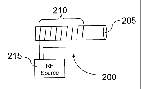
The boost
device 200 includes radio frequency coils 210 electrically coupled to an RF
generator 215.
The boost device 210 is configured to provide radio frequency signals into the
chamber 205.
The exact frequency and power may vary depending on numerous factors
including, but not
limited to, the desired effect, the configuration of the chamber, etc. In
certain examples, the
boost device provides signals at a frequency of about 25 MHz to about 50 MHz,
more
particularly about 35 MHz to about 45 MHz, e.g., about 40.6 MHz. In other
examples, the
boost device provides signals at a frequency of about 5 MHz to about 25 MHz,
more
particularly about 7.5 to about 15 MHz, e.g., about 10.4 MHz. In yet other
examples, the
23
CA 02608528 2013-09-18
54592-1
frequency ranges from about 1 kHz to about 100 GHz. For example, at lower
frequencies the
energy may be inductively coupled with the use of load coils or induction
coils, such as those
described in commonly owned U.S. Application Publication No. US 20040169855.
At most frequencies,
the energy may be capacitively coupled using plates or conductive coatings. At
high
frequencies, helical resonators or cavities may be used. Other suitable
frequencies will be
readily selected by the person of ordinary skill in the art, given the benefit
of this disclosure,
for various applications. In certain examples, the boost device may provide
radio
frequencies at a power of about 1 Watt to about 10,000 Watts, more
particularly about 10
to Watts to about 5,000 Watts. In other examples, the boost device provides
radio frequencies
at a power of about 100 Watts to about 2,000 Watts. In examples where a plasma
is formed
in a small capillary, such as a GC capillary tube.using a dry gas, then a
power of 1 watt or
less may be used. If a large secondary chamber, e.g., having dimensions
similar to a large
fluorescent light tube, and high solvent loads are used, then powers as large
as 10,000 watts
or higher may be desirable to provide the desired results. Other suitable
powers will be
readily selected by the person of ordinary skill in the art, given the benefit
of this disclosure.
Suitable devices for providing radio frequency signals include, but are not
limited to, radio
frequency transmitters commercially available from numerous sources such as
ENI, Trazar,
Hunttinger and Nautel, and radio frequency circuits such as Impedance Matching
Networks
from ENI, or Trazar. Suitable circuitry for generating radio frequencies will
be readily
selected and/or designed by the person of ordinary skill in the art, given the
benefit of this
disclosure. In some examples, two or more radio frequency coils are used with
each radio
frequency coil being tuned to the same frequency or a different frequency
and/or providing
radio frequencies at the same power or a different power. Other configurations
will be
selected by the person of ordinary skill in the art, given the benefit of this
disclosure.
[162] In accordance with certain examples, the boost devices disclosed here
may be
configured to provide additional energy to "boost" or increase the energy
already present in
a chamber, such as the chamber of an atomization device that includes an
atomization
source. As used here, "atomization device" is used in the broad sense and is
intended to
include other processes that may take place in the chamber, such as
desolvation,
vaporization, ionization, excitation, etc. Atomization source refers to a heat
source that is
operative to atomize, desolvate, ionize, excite, etc. species introduced into
the atomization
source. Suitable atomization sources for various applications will be readily
selected by the
24
CA 02608528 2007-11-14
WO 2006/138441
PCT/US2006/023277
person of ordinary skill in the art, given the benefit of this disclosure, and
exemplary
atomization sources include, but are not limited to, flames, plasmas, arcs,
sparks, etc.
[163] Without wishing to be bound by any particular scientific theory or by
this example,
understanding of certain aspects may be had with reference to the introduction
of a liquid
sample. As liquid sample is introduced into an atomization device, an
atomization source
within the chamber may rapidly cool, due to desolvation. That is, a material
amount of
energy may be used to convert the liquid solvent into a gas, which may result
in a decrease
in temperature (or other loss of energy) of the atomization source. A result
of this cooling is
that less energy may be available to atomize, ionize and/or excite any species
that were
dissolved in the solvent. Using certain embodiments of boost devices disclosed
here,
additional energy may be provided to enhance atomization and/or ionization of
any species
present in the introduced sample and, in certain examples, the additional
energy may be
used to excite atoms and/or ions present in a sample. For example, referring
to FIG. 2A and
without wishing to be bound by any particular scientific theory or application
or this one
embodiment, atomization device 300 includes A chamber 305 that is surrounded
by an
induction coil 310 in communication with a radio frequency generator 315.
Atomization
source is shown in a first state 320 and is contained within chamber 305. In
the example
shown in FIG. 2A, the radio frequency generator 315 is turned off such that no
radio
frequencies are provided to radio frequency coils 310. Referring now to FIG.
2B, when
radio frequency generator 315 is turned on, radio frequencies are provided to
chamber 305,
which results in conversion of the atomization source from the first state 320
to a second
state 330. A result of application of radio frequencies to chamber 305 is the
extension of
the atomization source along the axial and/or radial lengths of the chamber to
provide an
increased effective area of energy for atomizing, ionizing and exciting a
sample.
[164] In accordance with certain examples, an additional example of adding
energy to
enhance atomization and/or ionization of chemical species is shown in FIGS. 2C
and 2D.
Referring to FIG. 2C, a high frequency source 250, which may be, for example,
a 2.54
gigahertz magnetron, may be configured to be electrically coupled with a power
supply 252
and a waveguide adapter 254. An electrical lead 256 provides electrical
communication
between a waveguide adapter 254 and a circulator 258, which itself may be
electrically
coupled to a coaxial resistor load 260, e.g., a 50 ohm load. The circulator
258 is in
electrical communication with a microwave cavity 262, which is operative to
provide radio
frequencies into a chamber 264, which passes through the microwave cavity 262.
In FIG.
2C, the high frequency source 250 is turned off so that no radio frequencies
are transmitted
=
CA 02608528 2007-11-14
WO 2006/138441
PCT/US2006/023277
to the microwave cavity 262 or the chamber 264 and the atomization source
remains in a
first state 266. Referring now to FIG. 2D, when the high frequency source 250
is turned on,
radio frequencies are provided to the chamber 264, which results in conversion
of
atomization source from a first state 266 to a second state 268. A result of
application of
radio frequencies to the chamber 264 is the extension of the atomization
source along the
axial and/or radial lengths of the chamber to provide an increased effective
area of energy
for atomizing, ionizing and exciting a sample. Suitable commercially available
devices for
implementing the configurations shown in FIGS. 2A-2D will be readily selected
by the
person of ordinary skill in the art, given the benefit of this disclosure, and
illustrative
Hi microwave generators and power supplies are commercially available from
Aalter Reggio
Emlia (Italy), illustrative coaxial resistors are commercially available from
Bird Electronic
Corp. (Solon, OH), and illustrative circulators are commercially available
from National
Electronics (Geneva, Illinois). Illustrative waveguide adapters may be
fabricated, for
example, using cross-bar mode transducers, which are commercially available
from
numerous sources, and by reference to numerous publications, such as, for
example, the
"ITT Reference Data for Radio Engineers (Sixth Edition)" section under
"Waveguides and
Resonators." Microwave cavities may be commercially obtained from numerous
sources or
will be readily fabricated by the person of ordinary skill in the art, given
the benefit of this
disclosure, and optionally with the guidance of C. J. M. Beenakker,
Spectrochimica Acta,
Vol. 31B, pp. 483 to 486 Pergamon Press 1976.
[165] In accordance with certain examples, the person of ordinary skill in the
art, given the
benefit of this disclosure, may be able to extend the length of an atomization
source by a
selected or suitable amount. In certain examples, the length of the
atomization source may
be extended by using the boost devices. As one example, the atomization source
may be
extended by at least about three times its normal length along a longitudinal
axis of a
chamber using a boost device as disclosed herein. In other embodiments, the
atomization
source may be extended by at least about five times its normal length along
the longitudinal
axis of the chamber or at least about ten times it normal length along the
longitudinal axis of
the chamber using a boost device as disclosed herein.
[166] In accordance with certain examples, the boost devices may be operated
in a pulsed
or continuous mode. As used here pulsed mode refers to providing radio
frequencies in a
non-continuous manner by providing radio frequencies followed by a delay
before any
subsequent radio frequencies are provided to the chamber. For example,
referring to FIGS.
3A and 3B, channel A represents radio frequencies provided to a chamber, such
as chamber
26
CA 02608528 2013-09-18
545.92-1
205 shown in FIG. 1. Channel B represents the time intervals in which any
resulting signal
is measured from the chamber, using, for example, a detector such as those
discussed
herein. The example shown in FIG. 3A is based on sampling of a detectable
signal when
radio frequencies are not provided. Without wishing to be bound by any
particular
scientific theory or this example, by sampling any detectable signal during
periods where no
radio frequencies are provided, higher signal-to-noise values may be achieved.
It is
possible, however, to sample a detectable signal from a species during periods
where radio
frequencies are provided. For example and referring to FIG. 3B, in a
continuous mode, the
radio frequencies are provided continuously and any resulting signal may be
monitored
to continuously or intermittently. It will be within the ability of the
person of ordinary skill in
the art, given the benefit of this disclosure, to collect suitable signals
during and/or between
applications of radio frequencies using the boost devices disclosed herein.
[167] In accordance with certain other examples, an additional example of a
boost device
is shown in FIGS. 4A and 4B. In the configuration shown in FIGS. 4A and 4B, a
boost
device 400 includes a support or plate 405, a first electrode 410 and a second
electrode 420
each mounted to support 405. Each of the first electrode 410 and the second
electrode 420
may be configured to receive a chamber within the interior of the electrodes.
The support
or plate 405 may be electrically coupled to a radio frequency transmitter or
generator to
provide radio frequencies to the first electrode 410 and the second electrode
420. In this
example, the first electrode 410 and the second electrode 420 may be operated
at the same
frequency or may be individually tuned to provide different frequencies.
[168] In certain examples, the first electrode 410 may be operated with a
radio frequency
of about 10 MHz to about 2.54 GHz, and in other examples the second electrode
420 may
be operated with a radio frequency of about 100 kHz to about 2.54 GHz. In
other examples,
the first electrode 410 may be operated with radio frequencies from about 10
MHz to about
200NrHz, and second electrode 420 may be operated with radio frequencies from
about 100
kHz to about 200 MHz. The first electrode 410 and the second electrode 420 may
take the
form of the induction coil shown below in FIG. 9 or the induction coils
discussed in commonly
assigned patent applications with publication number US 20040169855 filed on
December 9,
2003, and entitled "1CP-OES and ICP-MS Induction Current". For the first
electrode 410 and
for the second electrode 420, radio frequencies from about 20 MHz to about 500
MHz may be
provided using, for example, helical resonators, an example of which is shown
in FIG. 9B and is
discussed in more detail below. In some examples, the first electrode 410
27
CA 02608528 2007-11-14
WO 2006/138441
PCT/US2006/023277
and the second electrode 420 may be operated using radio frequencies from
about 500 MHz
to about 5 GHz using a microwave cavity or resonant cavity, an example of
which is shown
in FIG. 2C. In certain examples, capacitive coupling of energy may also be
used in place of
second electrode 420; an example of this configuration is shown in FIG. 14B
and is
described in more detail below. Other suitable radio frequencies and powers
will be readily
selected by the person of ordinary skill in the art, given the benefit of this
disclosure.
[169] In accordance with certain examples, an example of an atomization device
is shown
in FIG. 5. Atomization device 500 includes a chamber 505, a flame source 510,
and a boost
device 520. The boost device 520 is electrically coupled to support 530, which
itself may
be electrically coupled to radio frequency transmitter or generator or both
(not shown). The
chamber 505 may be constructed of suitable materials, such as quartz, and may
include a
cooling tube or jacket (not shown) to surround the chamber to reduce the
temperatures
experienced by the boost device. In this example, the flame source 510 may be
any suitable
flame, such as a methane/air flame, a methane/oxygen flame, hydrogen/air
flame, a
hydrogen/oxygen flame, an acetylene/air flame, an acetylene/oxygen flame, an
acetylene/nitrous oxide flame, a propane/air flame, a propane/oxygen flame, a
propane/nitrous flame, a naphtha/air flame, a naphtha/oxygen flame, a natural
gas/nitrous
flame, a natural gas/air flame, a natural gas/oxygen flame and other flames
that may be
generated using a suitable fuel source and a suitable oxidant gas. Such flames
may
generally be created by introducing fuel and oxygen in selected ratios and
igniting the
mixture with a spark, arc, flame or the like. The exact temperature of the
flames may vary
depending on the fuel and oxidant gas source and depending on the distance
from the burner
tip. For example, the highest flame temperatures are typically found slightly
above the
primary combustion zone with lower temperatures in the interconal region and
in the outer
cone. In at least certain examples, the temperature of at least some portion
of the flame may
be at least about 1700 C. For example, a natural gas/air flame may have a
temperature of
about 1700-1900 C, whereas a natural gas/oxygen flame may have a temperature
of about
2700-2900 C and a hydrogen/oxygen flame may have a temperature of about 2550-
2700
C. Without wishing to be limited thereby, flame sources may be efficient at
desolvation in
some applications, but inefficient at atomization and ionization due to
relatively low
temperatures. Using the boost devices disclosed here, however, the efficiency
of ionization
and/or atomization may be increased using flame sources, such as
hydrogen/oxygen flames,
in combination with a boost device. For example, using one or more boost
devices
disclosed here in combination with a hydrogen/oxygen flame, it may be possible
to achieve
28
CA 02608528 2007-11-14
WO 2006/138441
PCT/US2006/023277
the benefits of having a high heat capacity of a flame for desolvation and
(e.g., followed by)
extreme plasma temperatures for greater excitation. This result is
advantageous for several
reasons including, but not limited to, reduced operating costs, simpler
design, less RF noise,
better signal-to-noise ratios, etc., although not every embodiment will 'meet
or address one
or more of these advantages.
[170] In addition, a flame may tolerate increased sample loading while leaving
the RF
power from the boost device available for sample ionization. To minimize the
spectral
background of the flame while maintaining high gas purity, a "water welder"
may be used
to decompose any produced water to its elements of hydrogen and oxygen.
Suitable water
welders are commercially available, for example, from SRA (Stan Rubinstein
Assoc.) or
KingMech Co., LTD. The flame (in certain embodiments) also preferably should
not
present significant additional background signal than the background observed
with the
desolvation of aqueous samples. The person of ordinary skill in the art, given
the benefit of
this disclosure, will be able to design suitable atomization devices including
flame sources
and boost devices.
[171] In accordance with certain examples, when using the device shown in FIG.
5, a fluid
sample may be introduced into the flame to desolvate the sample. Desolvation
may (in
certain embodiments) be accomplished by spraying the species into the chamber
in the form
of a fine mist. Suitable devices for creating mists of species include
nebulizers such as
those commercially available from J.E. Meinhard Assoc. Inc or CPI
International. A fluid
sample may be introduced into a nebulizer and may be mixed with an aerosol
carrier gas,
such as argon, neon, etc. The carrier gas nebulizes the liquid sample droplets
to provide
finely divided droplets that may be carried into the atomization device. Other
suitable
devices for delivering samples to the atomization device will be readily
selected by the
person of ordinary skill in the art, given the benefit of this disclosure, and
illustrative
devices include, but are not limited to, a concentric nebulizer, a cross-flow
nebulizer, an
ultrasonic nebulizer and the like.
[172] In accordance with certain examples, as sample is introduced through a
nebulizer
into the atomization device shown in FIG. 5, fluid may be vaporized from the
sample by a
flame or a primary plasma. Chemical species in the sample may be atomized
and/or ionized
using the energy produced by the flame or the primary plasma. To increase the
efficiency
of atomization and/or ionization, the boost device may be used to provide
radio frequencies
to chamber 505. Boost device may be configured to provide additional energy
such that
energy lost due to desolvation is restored by the boost, and, in certain
examples, the total
29
CA 02608528 2007-11-14
WO 2006/138441
PCT/US2006/023277
energy in the chamber exceeds the amount of energy present when only a flame
or primary
plasma is used. Such additional energy increases the amount of species that
are atomized
and/or ionized, which increases the number of species available for detection.
In certain
examples, atomization devices including the boost devices disclosed here may
allow for the
use of reduced amounts of sample due to the higher efficiency of atomization
and
ionization.
[173] Another example of an atomization device is disclosed in FIG. 6.
Atomization
device 600 includes a chamber 605, a flame or primary plasma 610, and a boost
device 620.
The boost device 620 includes a support 630, which may be electrically coupled
to a radio
frequency transmitter or generator (not shown). In the configuration shown in
FIG. 6, the
boost device 620 has been positioned downstream from the flame or primary
plasma 610 in
the "ionization region" of chamber 605. As used here, for illustrative
purposes only, the
ionization region refers to the region of a chamber where signal is measured
or detected.
For example and again for illustrative purposes only, region 650 in FIG. 6 is
referred to in
some instances herein as the desolvation region and region 660 is referred to
in some
instances herein as the ionization region. It will be understood by the person
of ordinary
skill in the art, given the benefit of this disclosure, however, the
desolvation may occur at
least to some extent in the ionization region and detection of chemical
species may occur at
least to some extent in the desolvation region depending on the exact
configuration of the
device, and it will also be understood by the person of ordinary skill in the
art, given the
benefit of this disclosure, that there need not be fixed or discrete
boundaries that separate
the desolvation and ionization regions. As sample is introduced into the flame
or primary
plasma 605, the flame or primary plasma 605 desolvates, atomizes, ionizes
and/or excites
the sample. The atomized and/or ionized sample may be carried downstream
toward boost
device 620 using for example an assist or carrier gas such as nitrogen gas,
argon gas, etc.
The atoms and ions may not be excited when exiting the desolvation region and
in certain
embodiments provide little or no detectable signal. Using boost device 620,
atomized
and/or ionized sample that enters the ionization region may be excited to
provide a
detectable signal. For example, atoms and ions may be excited by the radio
frequencies
introduced by boost device 620 such that optical emission occurs, which may be
detected
using suitable detectors as discussed in more detail below. It will be within
the ability of
the person of ordinary skill in the art, given the benefit of this disclosure,
to position boost
devices at suitable positions along a chamber to provide a desired result such
as, for
example, atomization, ionization or excitation.
CA 02608528 2007-11-14
WO 2006/138441
PCT/US2006/023277
[174] In accordance with certain examples, an example of an atomization device
using an
electrothermal atomization source is shown in FIG. 7. An atomization device
700 includes
a chamber 705, an electrothermal atomizer 710, a boost device 720 and a radio
frequency
generator 730. Electrothermal atomizers, such as graphite tubes or cups,
atomize sample by
first evaporating liquid from the sample at a relatively low temperature
(e.g., about 1200 C)
and then ashing the sample at a higher temperature (e.g., about 2000-3000 C),
which
results in atomization of the sample. The atomized sample may be carried down
chamber
705 using a carrier gas, such as argon, nitrogen, etc., and may be excited for
detection using
the boost device 720. The person of ordinary, skill in the art, given the
benefit of this
disclosure, will be able to design atomization devices with electrothermal
atomizers and
boost devices.
[175] In accordance with certain examples, an example of an atomization device
using a
plasma is shown in FIG. 8. An atomization device 800 includes a chamber 805, a
plasma
810, and a boost device 820. The boost device 820 includes a support which may
be in
electrical communication with a radio frequendy generator 830. Without wishing
to be
bound by any particular scientific theory, plasmas suffer less than flames
from
interferences, such as oxide formation, because of the higher temperatures of
the plasmas.
In addition, spectra may be obtained from a plurality of sample species under
a single set of
conditions, which allows for measurement of many species simultaneously. The
higher
temperatures in the plasmas may also provide improved detection limits and be
useful for
detection of non-metal species. A plasma may be created when a gas, such as
argon, is
excited and/or ionized to form ions and electrons, and in certain instances
cations. The ions
may be maintained at high temperatures by using an external power source, such
as a DC
electrical source. For example, two or more electrodes may be positioned
around high
temperature argon ions and electrons to provide current between the electrodes
to maintain
the plasma temperature. Other suitable power Sources for sustaining plasmas
include, but
are not limited to, radio frequency induction coils, such as those used in
inductively coupled
plasmas, and microwaves, such as those used in microwave induced plasmas. For
convenience purposes only, an inductively coupled plasma device is described
below, but
the boost devices disclosed herein may be readily used with other plasma
devices.
[176] Referring to FIG. 9A, inductively coupled plasma device 900 includes
chamber 905
comprising three or more tubes, such as tubes 910, 920 and 930. The tube 910
is in fluid
communication with a gas source, such as argon, and a sample introduction
device. The
argon gas aerosolizes the sample and carries it into the desolvation and
ionization regions of
31
CA 02608528 2007-11-14
WO 2006/138441
PCT/US2006/023277
a plasma 940. The tube 920 may be configured to provide tangential gas flow
throughout
the tube 930 to isolate plasma 940 from the tube 930. Without wishing to be
bound by any
particular scientific theory, gas is introduced through inlet 950, and the
tangential flow acts
to cool the inside walls of center tube 910 and centers plasma 940 radially.
Radio
frequency inductions coils 960 may be in electrical communication with a radio
frequency
generator (not shown) and are configured to create plasma 940 after the gas is
ionized using
an arc, spark, etc. The person of ordinary skill in the art, given the benefit
of this
disclosure, will be able to select or design suitable plasmas including, but
not limited to
inductively coupled plasmas, direct current plasmas, microwave induced
plasmas, etc., and
suitable devices for generating plasmas are commercially available from
numerous
manufacturers including, but not limited to, PerkinElmer, Inc., Varian
Instruments, Inc.
(Palo Alto, CA), Teledyne Leeman Labs, (Hudson, NH), and Spectro Analytical
Instruments (Kleve, Germany). An exemplary device for providing radio
frequencies is
shown in FIG. 9B. A helical resonator 970 comprises an RF source 972, an
electrical lead
974, which typically is a coaxial cable, configured to provide electrical
communication with
a coil 976 in a resonant cavity 978. The resonant cavity 974 with the coil 978
may be
configured to receive a chamber. In certain examples, radio frequencies from
about 20
MHz to about 500 MHz may be provided using, for example, helical resonators.
Exemplary
dimensional information for construction of helical resonators may be found,
for example,
in the International Telephone and Telegraph, Reference Data for Radio
Engineers. Fifth
Edition. Referring again to FIG. 8, after creation of plasma 810 using, for
example
atomized and ionized argon and radio frequency induction coils 860, sample may
be
introduced into the plasma 810. Without wishing to be bound by any particular
scientific
theory or this example, desolvation of the sample may reduce the temperature
of the plasma
and may result in lesser amounts of energy available for atomization and
ionization. The
boost device 820 may be used to provide radio frequencies to boost the energy
in the plasma
to increase the efficiency of atomization and ionization. For example, the
boost device 820
may be positioned such that the energy in the desolvation region 840 is
increased to
promote more efficient desolvation which may provide more atoms and ions to
generate a
detectable signal in the ionization region 850. It will be within the ability
of the person of
ordinary skill in the art, given the benefit of this disclosure, to design
atomization devices
including plasmas and boost devices to enhance desolvation, atomization,
ionization and
excitation.
32
CA 02608528 2007-11-14
WO 2006/138441
PCT/US2006/023277
[177] In accordance with certain examples, another example of an atomization
device
including a plasma is shown in FIG. 10. An atomization device 1000 includes a
chamber
1005, a plasma 1010, and a boost device 1020. The boost device 1020 includes a
support
1030, which may be in electrical communication with a radio frequency
transmitter or
generator (not shown). The atomization device 1000 also includes radio
frequency
induction coils 1035 which are constructed and arranged to maintain plasma
1010, which is
shown as a torus. In this example the boost device 1020 is positioned
downstream from a
desolvation region 1040 in an ionization region 1050. Introduction of a sample
into plasma
1010 may result in a decrease in plasma temperature as energy in the plasma is
used to
desolvate the sample. This temperature decrease may reduce the efficiency of
ionization
and atomization and may reduce the number of ions and atoms that are excited.
Using the
boost device 1020, ions and atoms that travel down the chamber 1005 to the
ionization
region 1050 may be excited. For example, radio frequencies at about 11 MHz and
at a
power of about 1.2 kilowatts may be provided to an analytical region 1050 to
excite atoms
and ions present in the ionization region. The excited atoms may be detected
using suitable
methods such as optical emission spectroscopy. The ionization region may be
extended
almost indefinitely by placing one or more boost devices along the ionization
region of
chamber 1005. As discussed further below, the boost devices may be configured
in stages
and may be individually tuned to different frequencies and/or powers. The
person of
ordinary skill in the art, given the benefit of this disclosure, will be able
to detect excited
ions and atoms using the atomization devices disclosed here along with
suitable optics,
detectors and the like.
[178] In accordance with certain examples, the signal originating from excited
atoms
and/or ions may be viewed or detected at least two ways. An example of the
ionization
region of a chamber, such as those used in the atomization devices disclosed
here, is shown
in FIGS. 11A and 11B. Any signal from a chamber 1105 may be viewed in at least
one of
two directions - axially or radially. Referring to FIG. 11A, when monitored or
detected
radially, signal from the chamber 1105 may be monitored in one or more planes
parallel to
the radius of the chamber 1105. For example, in an instrument configured to
measure
optical emissions radially, a detector may be positioned to detect signals
that are emitted in
the direction of arrow X in FIG. 11A. Referring to FIG. 11B, when detected or
monitored
axially, signal from the chamber 1105 may be monitored or detected in one or
more planes
parallel to the axis of the chamber. For example, in an instrument configured
to measure
optical emissions axially, a detector may be positioned to detect signals that
are emitted in
33
CA 02608528 2007-11-14
WO 2006/138441
PCT/US2006/023277
the direction of arrow Y in FIG. 11B. It will be recognized by the person of
ordinary skill
in the art, given the benefit of this disclosure, that axial and radial
detection are not limited
to optical emissions but may be used to detect signals from numerous other
analytical
techniques including absorption, fluorescence, phosphorescence, scattering,
etc.
[179] In accordance with certain examples, an atomization device that includes
at least
two boost devices is shown in FIG. 12. An atomization device 1200 may include
a
chamber 1205 and a radio frequency induction coil 1210 configured to generate
a plasma
1215. The atomization device 1200 may also include a first boost device 1220
in electrical
communication with a support 1230 and a second boost device 1240 in electrical
communication with a support 1250. In the example shown in FIG. 12, a first
boost device
1230 and a second boost device 1250 are positioned in the ionization region of
the chamber
1205 to provide additional energy to excite atoms and ions present in the
ionization region.
The boost devices 1230 and 1250 may be configured to provide the same or
different
frequency of radio frequencies. For example, each of boost devices may be
configured to
provide radio frequencies of about 15 MHz and at a power of about 1000 Watts.
The boost
devices 1230 and 1250 may independently provide radio frequencies in either
pulsed or
continuous modes. For example, the boost device 1230 may provide radio
frequencies in a
pulsed mode while the boost device 1250 may provide radio frequencies
continuously. In
the alternative, the boost device 1230 may provide radio frequencies
continuously while the
boost device 1250 may provide radio frequencies in a pulsed mode. In other
examples, both
of boost devices 1230 and 1250 may provide radio frequencies continuously, or
both of
boost devices 1230 and 1250 may provide radio frequencies in a pulsed mode. It
will be
within the ability of the person of ordinary skill in the art, given the
benefit of this
disclosure, to provide radio frequencies in a selected manner or mode using
multiple boost
devices. While the configuration shown in FIG. 12 includes two boost devices
positioned in
the ionization region of chamber 1205, in certain examples one of the boost
devices may be
positioned in the desolvation region with the second boost device positioned
in the
ionization region. In yet other examples, both of the boost devices may be
positioned in the
desolvation region. Additional configurations for arranging two or more boost
devices
along a chamber will be readily selected by the person of ordinary skill in
the art, given the
benefit of this disclosure.
[180] In accordance with certain examples, a chamber comprising a manifold or
interface
is disclosed. Referring to FIG. 13A, a chamber 1300 comprises a manifold or
interface
1305 in contact with a chamber cavity 1310. As shown in FIG. 13B, the
interface 1305
34
CA 02608528 2007-11-14
WO 2006/138441
PCT/US2006/023277
includes a small opening or a port 1320 configured to receive sample. The port
1320 may
take numerous sizes and forms. In certain examples, the port may be circular
and have a
diameter of about 0.25 mm to about 25 mm, more particularly about 4 mm. In
other
examples, the port may be rectangular with length and width measurements each
about 0.25
mm to about 4 mm. Other port shapes, such as rhomboidal, trapezoidal,
triangular,
octahedral, etc., and port sizes will be readily selected by the person of
ordinary skill in the
art, given the benefit of this disclosure. In certain examples, the port may
be positioned
centrally, such as the position of port 1320 shown in FIG. 13B, whereas in
other examples,
the port may be positioned at any selected region or area of the interface. In
examples
where the port is positioned at the center of the interface, the discharge
from the atomization
source may be blocked, or partially blocked, by the interface. Without wishing
to be bound
by any particular scientific theory or this example, blockage of the discharge
may lower the
detection limit due to removal, or reduction, of background signal from the
discharge,
which may increase the signal-to-noise ratio. This result may be achieved with
both axial
and radial detection of signals from the chamber 1300. Also, the working
pressure of the
boosted discharge may have some effect on the spectral emission quality, and
may be
optimized for the specific operating conditions based on sample, hardware,
detection
schemes, etc. An example of one way to control the working pressure of the
secondary
chamber is by controlling the exit gas flow rate and selecting the interface
port size.
Another example is to select the port diameter and directly control the exit
gas pressure.
Another example may be to have a higher exhaust flow and provide an additional
bleed gas
into the chamber. The exact pressure and power may vary depending on numerous
factors
including, but not limited to, the desired effect, the configuration of the
chamber, etc.
[181] In accordance with certain examples, the chamber 1300 may include a
vacuum
pump (not shown) that may be operative to draw sample through the port 1320
into the
secondary chamber for detection. In certain examples, the interface may be
configured with
a side port or outlet that is in fluid communication with the second chamber.
A vacuum
pump may be coupled to the side port to draw sample into the chamber 1300. In
other
examples, sample diffuses or flows into the secondary chamber, because the
pressure in the
secondary chamber may be less than the pressure in the atomization source
chamber. For
example, pressures in chambers including flames are higher than atmospheric
pressure due
to the high flow rates of gases introduced into the chamber. Pressures in
plasmas may be
higher than atmospheric pressure due to the high flow rates of gases through
the chamber.
In certain examples, the pressure of the chamber with the interface is
approximately
CA 02608528 2007-11-14
WO 2006/138441
PCT/US2006/023277
atmospheric pressure such that atoms and ions may flow down a pressure
gradient from the
high pressure chamber where atomization and/or ionization has occurred to a
lower pressure
chamber, e.g., where excitation may occur through the use of a boost device as
disclosed
herein. The person of ordinary skill in the art, given the benefit of this
disclosure, will be
able to construct suitable chambers with interfaces for receiving and/or
detecting atoms and
ions generated using one or more atomization sources.
[182] In accordance with certain examples, an atomization device comprising
two or more
chambers and a flame or primary plasma source is disclosed. Referring to FIG.
14A, an
atomization device 1400 may include a first chamber 1405 and a second chamber
1410. A
flame or primary plasma source 1415 may be positioned within the first chamber
1405. The
second chamber 1410 may include an interface or manifold 1430 and a boost
device 1440,
which may be in electrical communication with a support 1450. In certain
examples, the
second chamber 1410 may also include a vacuum pump 1460 which may be
configured to
draw atomized or ionized species from the first chamber 1405 into the second
chamber
1410, whereas in other examples species flow or diffuse into the second
chamber 1410 from
the first chamber 1405. A vacuum pump 1460 may be in direct fluid
communication with
the second chamber 1410 or, in certain other examples, an additional interface
may be
positioned at the end of the second chamber 1410 and may be configured to
provide fluid
communication between the second chamber 1410 and the vacuum pump 1460. In the
example shown in FIG. 14A, as atoms and/or ions enter into second chamber
1410, boost
device 1440 may provide radio frequencies to excite the atoms and ions. As
discussed
herein, such radio frequencies may be provided in a continuous mode or a
pulsed mode.
Also as discussed herein, radio frequency pulses from the boost device 1440
may be varied
during detection of any atoms or species within the second chamber 1410. In
other
examples, as discussed in more detail below, the second chamber 1410 may also
include
one or more additional boost devices, or, in certain examples, the first and
second chamber
are each configured with at least one boost device. In some examples, the
atomization
device may include additional chambers any one or more of which may include a
boost
device. The person of ordinary skill in the art, given the benefit of this
disclosure, will be
able to design suitable atomization devices that include flame or primary
plasma sources
and multiple chambers some of which may include a boost device.
[183] In accordance with certain examples, capacitive coupling may be used to
provide
additional energy in place of the boost devices. = Referring to FIG. 14B an
axial view of a
configuration for capacitive coupling is shown. Conductive plates 1462 and
1464 may be
36
CA 02608528 2007-11-14
WO 2006/138441
PCT/US2006/023277
positioned around a chamber, such as a second chamber 1466, e.g., a quartz
tube or other
non-conductive material, and may be in electrical communication with a high
voltage RF
source 1468 through electrical leads 1472 and 1474. Capacitive coupling may
provide
sufficient energy to the chamber to excite and/or ionize atoms in the chamber
within the
conductive plates 1462 and 1464. Additional configurations using conductive
plates and
high energy RF sources will be readily selected by the person of ordinary
skill in the art,
given the benefit of this disclosure.
[184] In accordance with other examples, an atomization device comprising two
or more
chambers and a plasma source is provided. Referring to FIG. 15, an atomization
device
1500 may include a first chamber 1505 and a second chamber 1510. The first
chamber
1505 may be surrounded by a radio frequency induction coil 1520 which may be
configured
to generate a plasma 1530. The second chamber 1510 also may be configured with
a boost
device 1540 which may be in electrical communication with a support 1550. The
second
chamber 1510 may also include an interface 1560 that may be configured to
receive a
portion of atoms or ions from the first chamber 1505. In certain examples, the
second
chamber 1510 may also include a vacuum pump (not shown) which may be
configured to
draw atomized or ionized species from the first chamber 1505 into the second
chamber
1510, whereas in other examples species may flow or diffuse into the second
chamber 1510
from the first chamber 1595. In yet other examples, the second chamber 1510
may include
a second interface positioned opposite the interface 1560. The second
interface may be
configured to provide fluid communication between the second chamber 1510 and
a
vacuum pump 1570. In the example shown in FIG. 15, as atoms and/or ions enter
into the
second chamber 1510, the boost device 1540 may provide radio frequencies to
excite the
atoms and ions. As discussed herein, such radio frequencies may be provided in
a
continuous mode or a pulsed mode. Also as discussed herein, the radio
frequency power
may be varied during detection of any atoms or species within the second
chamber 1510. In
other examples, as discussed in more detail below, the second chamber may also
include
one or more additional boost devices, or, in certain examples, the first and
second chamber
are each configured with at least one boost device. In some examples, the
atomization
device may include additional chambers any one or more of which may include a
boost
device. The person of ordinary skill in the art, given the benefit of this
disclosure, will be
able to design suitable atomization devices that include plasma sources and
multiple
chambers some of which may include a boost device.
37
CA 02608528 2007-11-14
WO 2006/138441
PCT/US2006/023277
[185] In accordance with certain examples, an atomization device including a
first
chamber and a second chamber with multiple boost devices is shown in FIG. 16.
An
atomization device 1600 may include a first chamber 1605 and a second chamber
1610.
The first chamber 1605 may be surrounded by a radio frequency induction coil
1620 which
may be configured to generate a plasma 1630. The second chamber 1610 may be
configured with a first boost device 1640, which may be in electrical
communication with a
support 1650, and a second boost device 1660, which may be in electrical
communication
with a support 1665. The second chamber 1610 may also include an interface or
manifold
1670 that may be configured to receive a portion of atoms or ions from the
first chamber
1605. In certain examples, the second chamber 1610 may also include a vacuum
pump
1680 which may be configured to draw atomized or ionized species from the
first chamber
1605 into the second chamber 1610, whereas in other examples species may flow
or diffuse
into the second chamber 1610 from the first chamber 1605. In yet other
examples, the
second chamber 1610 may include a second interface positioned opposite the
interface
1670. The second interface may be configured to provide fluid communication
between the
second chamber 1610 and the vacuum pump 1680. In the example shown in FIG. 16,
as
atoms and/or ions enter into the second chamber 1610, the first boost device
1640 may
provide radio frequencies to excite the atoms and ions. The second boost
device 1660 may
also provide radio frequencies to excite atoms and ions in the second chamber
1610. The
radio frequencies supplied by first boost device 1640 and second boost device
1660 may be
the same or different. The radio frequencies from each of the boost devices
may be
provided in a continuous mode or a pulsed mode. Also, the radio frequency
power from
each boost device may be varied during detection of any atoms or species
within the second
chamber 1610. In other examples, the first chamber may also include one or
more boost
devices. In some examples, the atomization device may include additional
chambers any
one or more of which may include one or more boost devices. The person of
ordinary skill
in the art, given the benefit of this disclosure, will be able to design
suitable atomization
devices that include multiple chambers including one or more boost devices.
[186] In accordance with certain examples, an atomization device including a
single RF
generator in electrical communication with a radio frequency induction coil
and a boost
device is disclosed. Examples using a single radio frequency generator, e.g. a
single RF
source, may allow for operation of the radio frequency induction coil and
boost device at
different inductances to tailor or to tune the radio frequency induction coil
or boost device
or both for a particular region or area of the device. A specific example of
this
38
CA 02608528 2007-11-14
WO 2006/138441
PCT/US2006/023277
configuration is described in more detail below with reference to FIG. 96B.
Even though a
single radio frequency generator may be used, the induction coil and the boost
device may
be designed for different plasma impedances in each region with respect to its
location. For
example, the inductance value of the induction coil and the boost device may
be different to
provide devices having different properties and performance characteristics.
In other
examples, the properties of the induction coil and the boost device may be
varied by varying
the diameter, coupling or shape of each of the induction coil and the boost
device. For
example, the primary RF supply and each of the induction coil and the boost
device may be
configured to provide radio frequencies of about 40 MHz and at a power of
about 1100
Watts in the primary discharge and a power of about 400 watts in the boost
device region.
In some examples, two or more coils from a single RF Source may be used, for
example,
where the primary discharge is separated from the secondary boost region by an
interface
(as shown in FIG 96C). It will be within the ability of the person of ordinary
skill in the art,
given the benefit of this disclosure, to design atomization devices including
a single radio
frequency generator in electrical communication with a radio frequency
induction coil and
one or more boost devices.
Spectroscopic Devices
[187] In accordance with certain examples, a device for optical emission
spectroscopy
(OES) is shown in FIG. 17. Without wishing to be bound by any particular
scientific
theory, as chemical species are atomized and/or ionized, the outermost
electrons may
undergo transitions which may emit light (potentially including non-visible
light). For
example, when an electron of an atom is in an excited state, the electron may
emit energy in
the form of light as it decays to a lower energy state. Suitable wavelengths
for monitoring
optical emission from excited atoms and ions will be readily selected by the
person of
ordinary skill in the art, given the benefit of this disclosure. Exemplary
optical emission
wavelengths include, but are not limited to, 396.152 nm for aluminum, 193.696
nm for
arsenic, 249.772 nm for boron, 313.107 nm for beryllium, 214.440 nm for
cadmium,
238.892 nm for cobalt, 267.716 nm for chromium, 224.700 nm for copper, 259.939
nm for
iron, 257.610 nm for manganese, 202.031 nm for molybdenum, 231.604 nm for
nickel,
220.353 nm for lead, 206.836 nm for antimony, 196.206 nm for selenium, 190.801
nm for
tantalum, 309.310 nm for vanadium and 206.200 nm for zinc. The exact
wavelength of
optical emission may be red-shifted or blue-shifted depending on the state of
the species,
e.g. atom, ion, etc., and depending on the difference in energy levels of the
decaying
electron transition, as known in the art.
39
CA 02608528 2007-11-14
WO 2006/138441
PCT/US2006/023277
[188] In accordance with certain examples and referring to FIG. 17, OES device
1700
includes a housing 1705, a sample introduction device 1710, an atomization
device 1720,
and a detection device 1730. The sample introduction device 1710 may vary
depending on
the nature of the sample. In certain examples, the sample introduction device
1710 may be
a nebulizer that is configured to aerosolize liquid sample for introduction
into the
atomization device 1720. In other examples, the sample introduction device
1710 may be
an injector configured to receive sample that may be directly injected or
introduced into the
atomization device. Other suitable devices and methods for introducing samples
will be
readily selected by the person of ordinary skill in the art, given the benefit
of this disclosure.
The atomization device 1720 may be any one or more of the atomization devices
discussed
herein or other atomization devices that include .a boost device that the
person of ordinary
skill in the art, given the benefit of this disclosure, may readily design or
select. The
detection device 1730 may take numerous forms and may be any suitable device
that may
detect optical emissions, such as optical emission 1725. For example, the
detection device
1730 may include suitable optics, such as lenses, mirrors, prisms, windows,
band-pass
filters, etc. The detection device 1730 may also include gratings, such as
echelle gratings,
to provide a multi-channel OES device. Gratings such as echelle gratings may
allow for
simultaneous detection of multiple emission wavelengths. The gratings may be
positioned
within a monochromator or other suitable device for selection of one or more
particular
wavelengths to monitor. In certain examples, the detection device 1730 may
include a
charge coupled device (CCD). In other examples, the OES device may be
configured to
implement Fourier transforms to provide simultaneous detection of multiple
emission
wavelengths. The detection device may be configured to monitor emission
wavelengths
over a large wavelength range including, but not limited to, ultraviolet,
visible, near and far
infrared, etc. The OES device 1700 may further include suitable electronics
such as a
microprocessor and/or computer and suitable circuitry to provide a desired
signal and/or for
data acquisition. Suitable additional devices and circuitry are known in the
art and may be
found, for example, on commercially available OES devices such as Optima
2100DV series
and Optima 5000 DV series OES devices commercially available from PerkinElmer,
Inc.
The optional amplifier 1740 may be operative to increase a signal 1735, e.g.,
amplify the
signal from detected photons, and provides the signal to display 1750, which
may be a
readout, computer, etc. In examples where the signal 1735 is sufficiently
large for display
or detection, the amplifier 1740 may be omitted. In certain examples, the
amplifier 1740 is
a photomultiplier tube configured to receive signals from the detection device
1730. Other
CA 02608528 2007-11-14
WO 2006/138441
PCT/US2006/023277
suitable devices for amplifying signals, however, will be selected by the
person of ordinary
skill in the art, given the benefit of this disclosure. It will also be within
the ability of the
person of ordinary skill in the art, given the benefit of this disclosure, to
retrofit existing
OES devices with the atomization devices disclosed here and to design new OES
devices
using the atomization devices disclosed here. The OES devices may further
include
autosamplers, such as AS90 and AS93 autosamplers commercially available from
PerkinElmer, Inc. or similar devices available from other suppliers.
[189] In accordance with certain examples, a single beam device for absorption
spectroscopy (AS) is shown in FIG. 18. Without wishing to be bound by any
particular
scientific theory, atoms and ions may absorb certain wavelengths of light to
provide energy
for a transition from a lower energy level to a higher energy level. An atom
or ion may
contain multiple resonance lines resulting from transition from a ground state
to a higher
energy level. The energy needed to promote such transitions may be supplied
using
numerous sources, e.g., heat, flames, plasmas, arc, sparks, cathode ray lamps,
lasers, etc, as
discussed further below. Suitable sources for providing such energy and
suitable
wavelengths of light for providing such energy will be readily selected by the
person of
ordinary skill in the art, given the benefit of this disclosure.
[190] In accordance with certain examples and referring to FIG. 18, a single
beam AS
device 1800 includes a housing 1805, a power source 1810, a lamp 1820, a
sample
introduction device 1825, an atomization device = 1830, a detection device
1840, an optional
amplifier 1850 and a display 1860. The power source 1810 may be configured to
supply
power to the lamp 1820, which provides one or more wavelengths of light 1822
for
absorption by atoms and ions. Suitable lamps include, but are not limited to
mercury lamps,
cathode ray lamps, lasers, etc. The lamp may be pulsed using suitable choppers
or pulsed
power supplies, or in examples where a laser is implemented, the laser may be
pulsed with a
selected frequency, e.g. 5, 10, or 20 times/second. The exact configuration of
the lamp
1820 may vary. For example, the lamp 1820 may provide light axially along the
atomization device 1830 or may provide light radially along the atomization
device 1830.
The example shown in FIG. 18 is configured for axial supply of light from the
lamp 1820.
As discussed above, there may be signal-to-noise advantages using axial
viewing of signals.
The atomization device 1830 may be any of the atomization devices discussed
herein or
other suitable atomization devices including a boost device that may be
readily selected or
designed by the person of ordinary skill in the art, given the benefit of this
disclosure. As
sample is atomized and/or ionized in the atomization device 1830, the incident
light 1822
41
CA 02608528 2007-11-14
WO 2006/138441
PCT/US2006/023277
=
from the lamp 1820 may excite atoms. That is, some percentage of the light
1822 that is
supplied by the lamp 1820 may be absorbed by the atoms and ions in the
atomization device
1830. The remaining percentage of the light 1835 may be transmitted to the
detection
device 1840. The detection device 1840 may provide one or more suitable
wavelengths
using, for example, prisms, lenses, gratings and other suitable devices such
as those
discussed above in reference to the OES devices, for example. The signal may
be provided
to the optional amplifier 1850 for increasing the signal provided to the
display 1860. To
account for the amount of absorption by sample in the atomization device 1830,
a blank,
such as water, may be introduced prior to sample introduction to provide a
100%
transmittance reference value. The amount of light transmitted once sample is
introduced
into atomization chamber may be measured, and the amount of light transmitted
with
sample may be divided by the reference value to obtain the transmittance. The
negative
logio of the transmittance is equal to the absorbance. AS device 1800 may
further include
suitable electronics such as a microprocessor and/or computer and suitable
circuitry to
provide a desired signal and/or for data acquisition. Suitable additional
devices and
circuitry may be found, for example, on commercially available AS devices such
as
AAnalyst series spectrometers commercially available from PerkinElmer, Inc. It
will also
be within the ability of the person of ordinary skill in the art, given the
benefit of this
disclosure, to retrofit existing AS devices with the atomization devices
disclosed here and to
design new AS devices using the atomization devices disclosed here. The AS
devices may
further include autosamplers known in the art, such as AS-90A, AS-90plus and
AS-93plus
autosamplers commercially available from PerkinElmer, Inc.
[191] In accordance with certain examples and referring to FIG. 19, a dual
beam AS
device 1900 includes a housing 1905, a power source 1910, a lamp 1920, an
atomization
device 1965, a detection device 1980, an optional amplifier 1990 and a display
1995. The
power source 1910 may be configured to supply power to the lamp 1920, which
provides
one or more wavelengths of light 1925 for absorption by atoms and ions.
Suitable lamps
include, but are not limited to, mercury lamps, cathode ray lamps, lasers,
etc. The lamp
may be pulsed using suitable choppers or pulsed power supplies, or in examples
where a
laser is implemented, the laser may be pulsed with a selected frequency, e.g.
5, 10 or 20
times/second. The configuration of the lamp 1920 may vary. For example, the
lamp 1920
may provide light axially along the atomization device 1965 or may provide
light radially
along the atomization device 1965. The example shown in FIG. 19 is configured
for axial
supply of light from the lamp 1920. As discussed above, there may be signal-to-
noise
42
CA 02608528 2007-11-14
WO 2006/138441
PCT/US2006/023277
advantages using axial viewing of signals. The atomization device 1965 may be
any of the
atomization devices discussed herein or other suitable atomization devices
including a boost
device that may be readily selected or designed by the person of ordinary
skill in the art,
given the benefit of this disclosure. As sample is atomized and/or ionized in
the
atomization device 1965, the incident light 1925 from the lamp 1920 may excite
atoms.
That is, some percentage of the light 1925 that is supplied by the lamp 1920
may be
absorbed by the atoms and ions in the atomization device 1965. The remaining
percentage
of the light 1967 is transmitted to the detection device 1980. In examples
using dual beams,
the incident light 1925 may be split using a beam splitter 1930 such that some
percentage of
light, e.g., about 10% to about 90%, may be transmitted as a light beam 1935
to atomization
device 1965 and the remaining percentage of the light may be transmitted as a
light beam
1940 to lenses 1950 and 1955. The light beams may be recombined using a
combiner 1970,
such as a half-silvered mirror, and a combined signal 1975 may be provided to
the detection
device 1980. The ratio between a reference value and the value for the sample
may then be
determined to calculate the absorbance of the sample. The detection device
1980 may
provide one or more suitable wavelengths using, for example, prisms, lenses,
gratings and
other suitable devices known in the art, such as those discussed above in
reference to the
OES devices, for example. Signal 1985 may be provided to the optional
amplifier 1990 for
increasing the signal for provide to the display 1995. AS device 1900 may
further include
suitable electronics known in the art, such as a microprocessor and/or
computer and suitable
circuitry to provide a desired signal and/or for data acquisition. Suitable
additional devices
and circuitry may be found, for example, on commercially available AS devices
such as
AAnalyst series spectrometers commercially available from PerkinElmer, Inc. It
will be
within the ability of the person of ordinary skill in the art, given the
benefit of this
disclosure, to retrofit existing dual beam AS devices with the atomization
devices disclosed
here and to design new dual beam AS devices using the atomization devices
disclosed here.
The AS devices may further include autosamplers known in the art, such as AS-
90A, AS-
90plus and AS-93plus autosamplers commercially available from PerkinElmer,
Inc.
[192] In accordance with certain examples, a device for mass spectroscopy (MS)
is
schematically shown in FIG. 20. MS device 2000 includes a sample introduction
device
2010, an atomization device 2020, a mass analyzer 2030, a detection device
2040, a
processing device 2050 and a display 2060. The sample introduction device
2010, the
atomization device 2020, the mass analyzer 2030 and the detection device 2040
may be
operated at reduced pressures using one or more vacuum pumps. In certain
examples,
43 .
CA 02608528 2007-11-14
WO 2006/138441
PCT/US2006/023277
however, only the mass analyzer 2030 and the detection device 2040 may be
operated at
reduced pressures. The sample introduction device 2010 may include an inlet
system
configured to provide sample to the atomization device 2020. The inlet system
may include
one or more batch inlets, direct probe inlets and/or chromatographic inlets.
The sample
introduction device 2010 may be an injector, a nebulizer or other suitable
devices that may
deliver solid, liquid or gaseous samples to the atomization device 2020. The
atomization
device 2020 may be any one or more of the atomization devices including a
boost device
discussed herein. As discussed herein, the atomization device 2020 may be a
combination
of two or more atomization devices at least one of which includes a boost
device. The mass
analyzer 2030 may take numerous forms depending generally on the sample
nature, desired
resolution, etc. and exemplary mass analyzers are discussed further below. The
detection
device 2040 may be any suitable detection device that may be used with
existing mass
spectrometers, e.g., electron multipliers, Faraday cups, coated photographic
plates,
scintillation detectors, etc., and other suitable devices that will be
selected by the person of
ordinary skill in the art, given the benefit of this disclosure. The
processing device 2050
typically includes a microprocessor and/or computer and suitable software for
analysis of
samples introduced into MS device 2000. One or more databases may be accessed
by the
processing device 2050 for determination of the chemical identity of species
introduced into
MS device 2000. Other suitable additional devices known in the art may also be
used with
the MS device 2000 including, but not limited to, autosamplers, such as AS-
90plus and AS-
93plus autosamplers commercially available from PerkinElmer, Inc.
[193] In accordance with certain examples, the mass analyzer of MS device 2000
may take
numerous forms depending on the desired resolution and the nature of the
introduced
sample. In certain examples, the mass analyzer is a scanning mass analyzer, a
magnetic
sector analyzer (e.g., for use in single and double-focusing MS devices), a
quadrupole mass
analyzer, an ion trap analyzer (e.g., cyclotrons, quadrupole ions traps), time-
of-flight
analyzers (e.g., matrix-assisted laser desorbed ionization time of flight
analyzers), and other
suitable mass analyzers that may separate species with different mass-to-
charge ratios. The
atomization devices disclosed herein may be used with any one or more of the
mass
analyzers listed above and other suitable mass analyzers. In certain examples,
the
atomization device in an MS device is a single chamber inductively coupled
plasma with a
boost device. In other examples, the atomization device is a single chamber
flame source
with a boost device. In yet other examples, the atomization device may include
two or more
44
CA 02608528 2007-11-14
WO 2006/138441
PCT/US2006/023277
chambers in which at least one of the chambers comprises a boost device as
disclosed
herein.
[194] In accordance with certain other examples, the boost devices disclosed
here may be
used with existing ionization methods used in mass spectroscopy. For example,
electron
impact sources with boost devices may be assembled to increase ionization
efficiency prior
to entry of ions into the mass analyzer. In other examples, chemical
ionization sources with
boost devices may be assembled to increase ionization efficiency prior to
entry of ions into
the mass analyzer. In yet other examples, field ionization sources with a
boost device may
be assembled to increase ionization efficiency prior to entry of ions into the
mass analyzer.
In still other examples, the boost devices may be used with desorption sources
such as, for
example, those sources configured for fast atom bombardment, field desorption,
laser
desorption, plasma desorption, thermal desorption, electrohydrodynamic
ionization/desorption, etc. In yet other examples, the boost devices may be
configured for
use with thermospray ionization sources, electrospray ionization sources or
other ionization
sources and devices commonly used in mass spectroscopy. It will be within the
ability of
the person of ordinary skill in the art, given the benefit of this disclosure,
to design suitable
devices for ionization including boost devices for use in mass spectroscopy.
[195] In accordance with certain other examples, the MS devices disclosed here
may be
hyphenated with one or more other analytical techniques. For example, MS
devices may be
hyphenated with devices for performing liquid chromatography, gas
chromatography,
capillary electrophoresis, and other suitable separation techniques. When
coupling an MS
device that includes a boost device with a gas chromatograph, it may be
desirable to include
a suitable interface, e.g., traps, jet separators, etc., to introduce sample
into the MS device
from the gas chromatograph. When coupling an MS device to a liquid
chromatograph, it
may also be desirable to include a suitable interface to account for the
differences in volume
used in liquid chromatography and mass spectroscopy. For example, split
interfaces may be
used so that only a small amount of sample exiting the liquid chromatograph
may be
introduced into the MS device. Sample exiting from the liquid chromatograph
may also be
deposited in suitable wires, cups or chambers for transport to the atomization
devices of the
MS device. In certain examples, the liquid chromatograph may include a
thermospray
configured to vaporize and aerosolize sample as it passes through a heated
capillary tube.
In some examples, the thermospray may include its own boost device to increase
ionization
of species using the thermospray. Other suitable devices for introducing
liquid samples
from a liquid chromatograph into a MS device will be readily selected by the
person of
CA 02608528 2007-11-14
WO 2006/138441
PCT/US2006/023277
ordinary skill in the art, given the benefit of this disclosure. In certain
examples, MS
devices, at least one of which includes a boost device, are hyphenated with
each other for
tandem mass spectroscopy analyses. For example, one MS device may include a
first type
of mass analyzer and the second MS device may include a different or similar
mass
analyzer as the first MS device. In other examples, the first MS device may be
operative to
isolate the molecular ions, and the second MS device may be operative to
fragment/detect
the isolated molecular ions. It will be within the ability of the person of
ordinary skill in the
art, given the benefit of this disclosure, to design hyphenated MS/MS devices
at least one of
which includes a boost device.
[196] In accordance with certain examples, a device for infrared spectroscopy
(IRS) is
provided. An IRS device includes a sample introduction device and an
atomization device
coupled or hyphenated to the infrared spectrometer. The atomization device may
be any of
the atomization devices discussed herein or other suitable atomization devices
including a
boost device. The atomization device may be configured to provide atoms and/or
ions to
the infrared spectrometer for detection. The infrared spectrometer may be a
single or
double-beam spectrophotometer, an interferometer, such as those commonly used
to
perform Fourier transform infrared spectroscopy, etc.. and exemplary infrared
spectrometers
and devices for use in infrared spectrometers are described in U.S. Patent
Nos. 4,419,575,
4,594,500, and 4,798,464, the entire disclosure of each of which is
incorporated herein by
reference for all purposes. For illustrative purposes only, an example of a
single-beam
FTIR spectrometer 2110 coupled to an atomization device 2115 is shown in FIG.
21. The
spectrometer 2110 comprises a light source 2116, such as a HeNe laser, an
interferometer
flat mirror 2120, interferometer scan mirrors 2125, a dessicant box 2130, an
infrared light
source 2135, a beam splitter 2140, an interferometer flat mirror 2145, an
adjustable toroidal
window 2150, a fixed toroidal window 2175, a sample chamber 2160 with KBr
windows
2162 and 2163, fixed toroidal windows 2165 and 2170 and an infrared detector
2180. The
infrared spectrometer 2110 may employ a single interferometer for detection of
species
introduced into the sample chamber 2160. Sample may be atomized or ionized
using the
atomization device 2115 and introduced into the sample chamber 2160 through a
tube 2117,
which provides fluid communication between the atomization device 2115 and the
sample
chamber 2160. The tube 2117 may include cooling devices such that the
temperature of any
atoms or ions exiting the atomization device 2115 may be reduced prior to
entry into the
sample chamber 2160. After sample has entered into the sample chamber 2160, a
valve or
port (not shown) may be closed such that no additional sample exits or enters
into the
46
CA 02608528 2007-11-14
WO 2006/138441
PCT/US2006/023277
sample chamber. In certain examples, the sample chamber 2160 may include
temperature
control to maintain the sample at a selected temperature. After a suitable
number of scans
have been obtained, the valve or port may be opened such that sample may be
permitted to
exit the sample chamber 2160 and may go to waste (not shown). In other
examples, the
flow from the atomization device 2115 into the sample chamber 2160 may be
continuous.
Other configurations for introducing atomized and/or ionized samples from
atomization
devices into an infrared spectrometer will be readily selected by the person
of ordinary skill
in the art, given the benefit of this disclosure. In certain examples, the
infrared spectrometer
may be in electrical communication with a processing device 2190, such as a
microprocessor or computer, which may be used to perform any necessary Fourier
transforms and/or other desired data analyses, e.g., quantitative or
qualitative analyses.
Suitable devices for coupling the atomization devices with infrared
spectrometers will be
readily selected by the person of ordinary skill inthe art, given the benefit
of this disclosure,
and illustrative devices include, but are not limited to, capillary tubes,
quartz tubes and
other tubes. For example capillary ionization, may use very low power filament
boost
discharges and may be sustained in sub-millimeter bore quartz tubes, whereas
with large
secondary chambers with high solvent loads, or less expensive, low frequency
high power
RF sources, it may be desirable to use a very large secondary chamber diameter
that is
about 100 mm in diameter or larger.
[197] In accordance with certain examples, a device for fluorescence
spectroscopy (FLS),
phosphorescence spectroscopy (PHS) or Raman spectroscopy is shown in FIG. 22.
Device
2200 includes an atomization device 2205, a light source 2210, a sample
chamber 2220, a
detection device 2230, an optional amplifier 2240 and a display 2250. The
detection device
2230 may be positioned ninety degrees from incident light 2212 from the light
source 2210
to minimize the amount of light from the light source 2210 that arrives at the
detection
device 2230. Fluorescence, phosphorescence and Raman emissions may occur in
360
degrees so the positioning of the detection device 2230 to collect light
emissions is not
critical. The atomization device 2205 may be any of the atomization devices
discussed
herein and other atomization devices configured with at least one boost de
vice. The
atomization device 2205 may be configured to provide atoms and ions to the
sample
chamber 2220 through the tube 2222 which may be in fluid communication with
the sample
chamber 2220. An optical chopper 2215 may be used where it is advantageous to
pulse the
light source 2210. Where the light source is a pulsed laser, the chopper 2215
may be
omitted. As atomized and/or ionized sample enters into the sample chamber
2220, the light
47
CA 02608528 2007-11-14
WO 2006/138441
PCT/US2006/023277
source 2210 excites one or more electrons into an excited state, e.g., into an
excited singlet
state, and the excited atom may emit photons as it decays back to a ground
state. Where the
excited atom decays from an excited singlet state to the ground state with
resultant emission
of light, fluorescence emission is said to occur, and the maximum emission
signal is
typically red-shifted when compared to the wavelength of the excitation
source. Where the
excited atom decays from an excited triplet state to the ground state with
resultant emission
of light, phosphorescence emission is said to occur, and the maximum emission
wavelength
of phosphorescence is typically red-shifted when compared to the fluorescence
maximum
emission wavelength. For Raman spectroscopy, scattered radiation may be
monitored and
the Stokes or anti-Stokes lines may be monitored to provide detection of the
sample. The
emission signal may be collected using the detection device 2230, which may
be, for
example, a monochromator with suitable optics such as prisms, echelle gratings
and the
like. The detection device 2230 provides a signal to the optional amplifier
2240 for
amplification of the signal, which may then be viewed using the display 2250.
In examples,
where the signal is sufficiently strong for detection, the optional amplifier
2240 may be
omitted. In certain examples, the display 2250 is part of a computer or data
acquisition
system for analysis of the signals.
[198] In accordance with certain examples, the sample chamber conditions may
be varied
depending on whether it is desirable to measure fluorescence, phosphorescence
or Raman
scattering. For many chemical species, the rate constant for internal
conversion and/or
fluorescence is typically much greater than the rate constant for
phosphorescence and, as a
result, either non-radiative emission or fluorescence emission dominates. By
varying the
sample conditions, it may be possible to favor phosphorescence, or scattering,
over
fluorescence. For example, the sample chamber 2220 may include a matrix or
solid
support, e.g., silica, cellulose, acrylamide, etc., that atoms and/or ions may
be adsorbed to or
trapped in. In other examples, the sample chamber 2220 may be operated at
reduced
temperatures, e.g., 77 Kelvin, such that atoms and ions entering into the
sample chamber
2220 may be frozen in a matrix. For at least certain species, immobilization
of the species
in a matrix may result in increased intersystem crossing to populate triplet
energy levels,
which may favor phosphorescence emission over fluorescence emission. It will
be within
the ability of the person of ordinary skill in the art, given the benefit of
this disclosure, to
select suitable sampling conditions for monitoring fluorescence,
phosphorescence and
Raman scattering.
48
CA 02608528 2007-11-14
WO 2006/138441
PCT/US2006/023277
[199] In accordance with certain examples, a device for performing X-ray
spectroscopy
that includes a boost device is disclosed. An atomization device including a
boost device
may be configured to provide atoms and ions to the sample chamber. Once in the
sample
chamber, the ions and atoms may be subjected to an X-ray source and X-ray
absorption or
emission may be monitored. Suitable instruments known in the art for
performing X-ray
spectroscopy include, for example, PHI 1800 XPS commercially available from
Physical
Electronics USA. It will be within the ability of the person of ordinary skill
in the art, given
the benefit of this disclosure, to adapt the boost devices disclosed here for
use in X-ray
spectroscopic techniques.
[200] In accordance with certain examples, a gas chromatograph comprising a
boost
device is shown in FIG. 23. A gas chromatograph 2300 includes a carrier gas
2310 in fluid
communication with an injector 2320. The flow rate of the carrier gas 2310 may
be
regulated using, for example, a pressure regulator, flow meter, etc. The flow
of the carrier
gas 2310 may be split using a flow splifter 2315 such that a portion of the
carrier gas 2310
passes through a tube in fluid communication with the injector 2310 and the
remaining
carrier gas 2310 may pass to waste. The gas chromatograph 2300 may further
include a
heating device 2330, such as an oven. The heating device 2330 may be operative
to
vaporize liquid sample injected through the injector 2320. In certain
examples, the heating
device 2330 may include an internal boost device to assist with vaporization.
Within the
heating device 2330 is at least one column 2340 which may separate species
within an
introduced sample. The column 2340 includes one or more stationary phases such
as, for
example, polydimethyl siloxane, poly(phenylmethyldimethyl) siloxane,
poly(phenylmethyl)
siloxane, poly(trifluoropropyldimethypsiloxane,
polyethylene glycol,
poly(dicanoallyldimethyl) siloxane and other stationary phases commercially
available from
numerous manufacturers such as, for example, Phenomenex (Torrance, CA).
Separated
species may elute from the column 2340 and may flow into detector 2350. The
detector
2350 may be any one or more of detectors commonly used in gas chromatography
including, but not limited to, flame ionization detectors, thermal
conductivity detectors,
thermionic detectors, electron-capture detectors, atomic emission detectors,
photometric
detectors, fluorescence detectors, photoionization detectors and the like. In
the example
shown in FIG. 23, the detector 2350 may include a boost device 2360, which may
be used
to promote ionization and/or excite ionized species in the detector 2350. It
will be within
the ability of the person of ordinary skill in the art, given the benefit of
this disclosure, to
configure gas chromatographs with suitable boost devices.
49
CA 02608528 2007-11-14
WO 2006/138441
PCT/US2006/023277
[201] In accordance with certain other examples, a gas chromatograph may be
hyphenated
or coupled to an additional instrument. In some examples, the gas
chromatograph may be
coupled to an inductively coupled plasma that includes a boost device. For
example, a gas
chromatograph may be used to vaporize and separate species in a sample such
that
individual species elute from the gas chromatograph. The eluted species may be
introduced
into an inductively coupled plasma that is hyphenated to the gas
chromatograph. The
inductively coupled plasma may include one or more boost devices for providing
radio
frequencies to promote atomization and/or ionization efficiency or for
providing radio
frequencies to excite atomized and/or ionized species. In other examples, a
gas
to chromatograph may be coupled to a mass spectrometer that includes a
boost device. For
example, a gas chromatograph may be used to vaporize and separate species in a
sample,
and the separated species may be introduced into a mass spectrometer for
fragmentation and
detection. In some examples, a gas chromatograph may be hyphenated to an
inductively
coupled plasma which itself is coupled to a mass spectrometer. Additional
devices and
instruments that include boost devices will be readily coupled to gas
chromatographs by the
person of ordinary skill in the art, given the benefit of this disclosure.
[202] In accordance with certain examples, a device for liquid chromatography
(LC), e.g.,
for performing LC, fast protein liquid chromatography (FPLC), high performance
liquid
chromatography (HPLC), etc., comprising a boost device is shown in FIG. 24. An
LC
device 2400 includes a carrier solvent reservoir 2410, a pump 2420, an
injector 2430, a
column 2450 and a detector 2460. In certain examples, additional pumps and
solvents may
be included so that solvent gradient techniques may be implemented during the
separation.
The carrier solvent generally depends on numerous factors including, but not
limited to, the
species in the sample to be separated and on the nature of the stationary
phase in the column
2450. The solvent(s) is typically degassed, e.g., using flitted filtration,
bubbling nitrogen
through the solvent, etc., prior to any separations. Suitable solvents for
performing a given
separation and methods for degassing the solvents will be readily selected by
the person of
ordinary skill in the art, given the benefit of this disclosure. The injector
2430 may be any
injector that is configured to provide reproducible injections and, in certain
examples, the
injector 2430 is a loop injector, such as those commercially available from
PerkinElmer,
Inc, Beckman Instruments and the like. As sample is injected into the injector
2430, solvent
carries sample into the column 2450 where separation of the species in the
sample may
occur. The exact stationary phase in the column 2450 may vary depending the
species to be
separated, the solvent composition, etc., and in certain examples, the
stationary phase may
CA 02608528 2007-11-14
WO 2006/138441
PCT/US2006/023277
be selected from C18 based stationary phases, silica, strong anion exchange
materials,
strong cation exchange materials, size exclusion media, and other stationary
phases
commonly used in LC, FPLC, and HPLC. Suitable stationary phases and LC columns
are
commercially available from numerous manufacturers such as, for example,
Phenomenex,
Inc. (Torrance, CA). The separated species may elute from the column 2450 and
enter into
the detector 2460. The detector 2460 may take numerous forms including, but
not limited
to, UV/Visible absorbance detectors, fluorescence detectors, conductivity
detectors,
electrochemical detectors, refractive index detectors, evaporative light
scattering detectors,
mass analyzers, nuclear magnetic resonance detectors, electron spin resonance
detectors,
circular dichroism detectors, etc. In certain examples, such as where the
liquid
chromatograph 2400 may be configured with a mass analyzer, the liquid sample
may be
nebulized, vaporized and atomized prior to introduction into the mass
analyzer. For
example, a chromatographic peak may be eluted= from the column 2450, and
vaporized and
atomized using, for example, an inductively coupled plasma prior to
introduction into the
mass analyzer. The inductively coupled plasma may include a boost device to
promote
ionization efficiency. It will be within the ability of the person of ordinary
skill in the art,
given the benefit of this disclosure to configure LC devices with the boost
devices disclosed
here.
[203] In accordance with certain other examples, an LC device may be
hyphenated or
coupled to an additional instrument. In some examples, the liquid
chromatograph may be
coupled to an inductively coupled plasma that includes a boost device. For
example, a
liquid chromatograph may be used to separate species dissolved in a liquid
sample, and the
eluted species may be introduced into an inductively coupled plasma that may
be
hyphenated to the liquid chromatograph and where atomization and/or detection
may occur.
The inductively coupled plasma may include one or more boost devices for
providing radio
frequencies to promote atomization and/or ionization efficiency or for
providing radio
frequencies to excite atomized and/or ionized species. In other examples, the
liquid
chromatograph may be coupled to a mass spectrometer that includes a boost
device. For
example, the liquid chromatograph may be used to separate species in a sample,
and the
separated species may be introduced into a mass spectrometer for fragmentation
and
detection. It may be desirable to vaporize, using, for example, an inductively
coupled
plasma with a boost device, a thermospray with a boost device, etc., the
liquid sample prior
to introduction into the mass spectrometer. Additional devices and instruments
that include
51
CA 02608528 2007-11-14
WO 2006/138441
PCT/US2006/023277
boost devices will be readily coupled to liquid chromatographs by the person
of ordinary
skill in the art, given the benefit of this disclosure.
[204] In accordance with certain examples, a device for nuclear magnetic
resonance
(NMR) including a boost device is disclosed. In certain examples, the NMR is
hyphenated
to one or more additional devices that include the boost device. For example,
species may
be analyzed using NMR and then subsequent to NMR analysis may be introduced
into an
atomization device with a boost device for detection. In other examples, the
species may
first be atomized using the atomization device with a boost device and then
the atoms
and/or ions may be analyzed using NMR. For example, gas phase NMR studies may
be
performed to identify impurities with a high vapor pressure. In certain
examples, it may be
necessary to pressurize the sample chamber, e.g., to about 10-50 atm, to
obtain good spectra
for gas phase species. For illustrative purposes only, a block diagram of an
NMR device
suitable for pulsed NMR experiments is shown in FIG. 25. An NMR device 2500
includes
a magnet 2510, an RF generator 2520, a receiver 2530, and a data acquisition
device 2540,
such as a computer. The magnet 2510 includes a field-frequency lock 2512 and
shim coils ,
2514 each of which may be in electrical communication with the data
acquisition device
2540. The probe 2516 may be positioned within the magnet 2510. The probe 2516
may be
electrically coupled to an RF transmitter 2522. The RF transmitter 2522 may be
in
electrical communication with a frequency synthesizer 2524. The frequency
synthesizer
2524 may be in electrical communication with a pulse programmer 2526. The RF
generator
2520 may be configured to provide RF pulses, e.g., ninety degree pulses, 180
degree pulses,
etc., to the probe 2516 for detection of species present in a sample contained
within the
probe 2516. When a signal is transmitted from the probe 2516, the signal may
be sent to the
receiver 2530 for detection. The receiver 2530 may include a preamplifier
2532, a phase
sensitive detector 2534, audio filters 2536 and an analog-to-digital converter
2538 for
providing a signal to the data acquisition system 2540. The probe may be
configured to
detect one or more magnetically active nuclei, e.g. 111, 13C, 15N, 31P, etc.
In certain
examples, the NMR device may be used for one, two, three, or four-dimensional
NMR
spectroscopic techniques, e.g., NOESY, COSY, TOCSY, etc. In certain examples,
an NMR
device may be hyphenated to an atomization device with a boost device that may
detect
atomized and/or ionized species. In other examples, the NMR device may be
hyphenated to
a mass analyzer, which itself may be coupled to an atomization device, for
analysis based
on mass-to-charge ratios. In certain examples, a tube or conduit may be
provided between
the probe of the MR device and the additional device, e.g., an ICP or a mass
analyzer,
52
CA 02608528 2007-11-14
WO 2006/138441
PCT/US2006/023277
such that sample may be automatically transferred from the NMR device to the
additional
device. The person of ordinary skill in the art, given the benefit of this
disclosure, will be
able to select or design suitable NMR devices for hyphenating additional
devices that
include boost devices.
[205] In accordance with additional example, a device for electron spin
resonance (ESR)
that is hyphenated to an additional device including a boost device is
provided. Without
wishing to be bound by any particular scientific theory, many metal species
that may be
detected by OES or AS may also be detected using ESR. For example, manganese
with a
spin number of 5/2 provides and ESR spectrum with 6 lines when free manganese
is
dissolved in water. The exact line shape and line widths of the ESR spectrum
may provide
some indication of the environment experienced by the manganese ions. The
optical
emission of atomic manganese may be detected at 257.610 nm. Using an ESR
instrument
hyphenated to an OES device, two measurements may be performed on the same
sample.
Suitable ESR instruments are commercially available from numerous
manufacturers
including, but not limited to, Bruker Instruments (Germany). The ESR may be
coupled
with an OES device using suitable tubing and connectors such that liquid
sample from the
ESR may be removed and delivered to the OES device without the need to
manually inject
sample into the OES device. It will be within the ability of the person of
ordinary skill in
the art, given the benefit of this disclosure, to couple ESR devices with
additional devices
and instruments including atomization devices with boost devices.
[206] In accordance with certain examples, a spectrometer configured for
measurement in
the low UV and that includes a boost device is provided. As used herein "low
UV" refers to
measurements taken at or around 90-200 nm or less. At wavelengths of less than
about
200-210 nm, oxygen in the optical path may absorb emitted light (in the case
of an OES
device) or may absorb light used to excite atoms and ions (in the case of an
AS device).
This absorption by the oxygen may prevent detection of emission lines of
atoms, such as
chlorine, that emit in the low UV range. By using a boost device with an OES
device or
with an AS device, low UV measurements may be obtained by eliminating any
oxygen
present in the optical path. This result may be accomplished, for example, by
coupling a
first chamber, or a second chamber, to the spectrometer. For example, a first
chamber may
be used to contain the atomization source, and an interface may be used to
draw atomized
sample into a second chamber. The second chamber may include a boost device.
The
second chamber may be in fluid communication with a window or aperture on the
spectrometer such that the optical path of the spectrometer is sealed off from
any outside air
53
CA 02608528 2007-11-14
WO 2006/138441
PCT/US2006/023277
or oxygen. The optical path may be purged with a gas that does not absorb in
the low UV,
e.g., nitrogen, such that light emissions in the low UV, or light absorptions
using low UV,
are not interfered with by oxygen. In certain examples, the device includes a
boost device
optically coupled to a window on a spectrometer such that substantially no
oxygen or air
exists in the light path of the spectrometer. = In certain examples, the
device may be
configured for optical emission such that light emissions in the low UV may be
detected. In
other examples, the device may be configured for atomic absorption such that
species that
absorb low UV light may be detected. In certain examples, the detector may be
optically
coupled to a chamber comprising a boost device such that light emissions or
absorptions in
the chamber may be detected. In some examples, the chamber may also be
optically
coupled to a light source, e.g., a UV light source such as a laser, arc lamp
or the like, such
that light may be provided to the chamber to detect the presence of species
that absorb the
low UV light. Illustrative configurations of low UV devices are described in
more detail
below in Examples 7 and 8 herein.
[207] In other examples, an OES device with an inductively coupled plasma and
a boost
device and configured to detect metal species at levels at least about five-
times less, more
particularly at least ten times less, than detection levels obtainable using
non-boosted ICP-
OES devices is disclosed. Without wishing to be bound by any particular
scientific theory,
the boost devices disclosed here may increase the area of the emission region
of OES
devices by 5-fold, 10-fold or more. In certain examples using the RF boost
devices
disclosed herein, the emission region of OES devices increases by about 5-
fold, 10-fold or
more without a substantial increase in background emission. While in some
examples the
background signal may increase, the increase in background signal may be
proportionately
lower than the increase in emission signal intensity to provide lower
detection levels. Such
an increase in signal area may result in lowering of the OES detection limit
of metals by at
least about 5-fold, 10-fold or more. It will be within the ability of the
person of ordinary
skill in the art, given the benefit of this disclosure, to use OES devices
that include boost
devices to detect metal species at levels of at least about 5-times less than
non boosted ICP-
OES devices.
[208] In accordance with yet other examples, an OES device with an inductively
coupled
plasma and a boost device and configured to detect aluminum at a level of
about 0.18 [tg/L
or less is provided. As discussed herein, the boost devices disclosed here may
increase the
emission region of OES devices by 5-fold or more. In certain other examples,
the boost
devices disclosed herein may increase the emission region of OES devices by 5-
fold or
54
CA 02608528 2007-11-14
WO 2006/138441
PCT/US2006/023277
more without a substantial increase in background emission. Such an increase
may result in
lowering of the OES detection limit of aluminum (about 0.9 gip by at least 5-
fold. In
some examples, the OES device may be configured to detect aluminum at levels
of about
0.11 tig/L or less, e.g. 0.09 iug/L, 0.045 ptg/L or less. The OES device may
include, for
example, an atomization source and boost devices as disclosed herein, with
such examples
provided for illustration and not limitation.
[209] In accordance with certain other examples, an OES device with an
inductively
coupled plasma and a boost device and configured to detect arsenic at a level
of about 0.6
pig/L or less is provided. The boost devices disclosed here may increase the
emission
region of OES devices by 5-fold or more. In certain other examples, the boost
devices
disclosed herein may increase the emission region of OES devices by 5-fold or
more
without a substantial increase in background emission. Such an increase may
result in
lowering of the OES detection limit of arsenic (about 3.0-3.6 p,g/L) by at
least 5-fold. In
some examples, the OES device may be configured to detect arsenic at levels of
about 0.4
tig/L or less, e.g. 0.3 gg/L, 0.15m/L or less. The OES device may include, for
example, an
atomization source and boost devices as disclosed herein, with such examples
provided for
illustration and not limitation.
[210] In accordance with other examples, an OES device with an inductively
coupled
plasma and a boost device and configured to detect boron at a level of about
0.05 pg/L or
less is provided. The boost devices disclosed here may increase the emission
region of OES
devices by 5-fold or more. In certain other examples, the boost devices
disclosed herein
may increase the emission region of OES devices by 5-fold or more without a
substantial
increase in background emission. Such an increase may result in lowering of
the OES
detection limit of boron (about 0.25-1.0 ttg/L) by at least 5-fold. In some
examples, the
OES device may be configured to detect boron levels of about 0.033 lig/L or
less, e.g. 0.025
pz/L, 0.0125 tig/L or less. The OES device may include, for example, an
atomization
source and boost devices as disclosed herein, with such examples provided for
illustration
and not limitation.
[211] In accordance with certain examples, an OES device with an inductively
coupled
plasma and a boost device and configured to detect beryllium at a level of
about 0.003 p.g/L
or less is provided. As discussed herein, the boost devices disclosed here may
increase the
emission region of OES devices by 5-fold or more. In certain other examples,
the boost
devices disclosed herein may increase the emission region of OES devices by 5-
fold or
more without a substantial increase in background emission. Such an increase
may result in
=
CA 02608528 2007-11-14
WO 2006/138441
PCT/US2006/023277
lowering of the OES detection limit of beryllium (about 0.017-1.0 g/L) by at
least 5-fold.
In some examples, the OES device may be configured to detect beryllium levels
of about
0.002 g/L or less, e.g. 0.0017 g/L, 0.00085 g/L or less. The OES device may
include,
for example, an atomization source and boost devices as disclosed herein, with
such
examples provided for illustration and not limitation.
[212] In accordance with certain examples, an OES device with an inductively
coupled
plasma and a boost device and configured to detect cadmium at a level of about
0.014 g/L
or less is provided. The boost devices disclosed here may increase the
emission region of
OES devices by 5-fold or more. In certain other examples, the boost devices
disclosed
herein may increase the emission region of OES devices by 5-fold or more
without a
substantial increase in background emission. Such an increase may result in
lowering of the
OES detection limit of cadmium (about 0.07-0.1 g/L) by at least 5-fold. In
some
examples, the OES device may be configured to detect cadmium levels of about
0.009 g/L
or less, e.g. 0.007 g/L, 0.0035 g/L or less. The OES device may include, for
example, an
atomization source and boost devices as disclosed herein, with such examples
provided for
illustration and not limitation.
[213] In accordance with certain examples, an OES device with an inductively
coupled
plasma and a boost device and configured to detect cobalt at a level of about
0.05 g/L or
less is provided. The boost devices disclosed here may increase the emission
region of OES
devices by 5-fold or more. In certain other examples, the boost devices
disclosed herein
may increase the emission region of OES devices by 5-fold or more without a
substantial
increase in background emission. Such an increase may result in lowering of
the OES
detection limit of cobalt (about 0.25 g/L) by at least 5-fold. In some
examples, the OES
device may be configured to detect cobalt levels of about 0.033 g/L or less,
e.g., 0.025
g/L, 0.01 g/L or less. The OES device may include, for example, an
atomization source
and boost devices as disclosed herein, with such examples provided for
illustration and not
limitation.
[214] In accordance with certain examples, an OES device with an inductively
coupled
plasma and a boost device and configured to detect chromium at a level of
about 0.04 g/L
or less is provided. The boost devices disclosed here may increase the
emission region of
OES devices by 5-fold or more. In certain other examples, the boost devices
disclosed
herein may increase the emission region of OES devices by 5-fold or more
without a
substantial increase in background emission. Such an increase may result in
lowering of the
OES detection limit of chromium (about 0.20-0.25 g/L) by at least 5-fold. In
some
56
CA 02608528 2007-11-14
WO 2006/138441
PCT/US2006/023277
examples, the OES device may be configured to detect chromium levels of about
0.03 g/L
or less, e.g., 0.02 g/L, 0.01 g/L or less. The OES device may include, for
example, an
atomization source and boost devices as disclosed herein, with such examples
provided for
illustration and not limitation.
[215] In accordance with certain examples, an OES device with an inductively
coupled
plasma and a boost device and configured to detect copper at a level of about
0.08 g/L or
less is provided. The boost devices disclosed here may increase the emission
region of OES
devices by 5-fold or more. In certain other examples, the boost devices
disclosed herein
may increase the emission region of OES devices by 5-fold or more without a
substantial
increase in background emission. Such an increase may result in lowering of
the OES
detection limit of copper (about 0.4-0.9 g/L) by at least 5-fold. In some
examples, the
OES device is configured to detect copper levels of about 0.053 g/L or less,
e.g., 0.04
g/L, 0.02 g/L or less. The OES device may include, for example, an
atomization source
and boost devices as disclosed herein, with suck examples provided for
illustration and not
limitation.
[216] In accordance with certain examples, an OES device with an inductively
coupled
plasma and a boost device and configured to detect iron at a level of about
0.04 g/L or less
is provided. As discussed herein, the boost d evices disclosed here may
increase the
emission region of OES devices by 5-fold or more. In certain other examples,
the boost
devices disclosed herein may increase the emission region of OES devices by 5-
fold or
more without a substantial increase in background emission. Such an increase
may result in
lowering of the OES detection limit of iron (about 0.2-0.4 g/L) by at least 5-
fold. In some
examples, the OES device may be configured to detect iron levels of about
0.027 g/L or
less, e.g., 0.02 g/L, 0.01 g/L or less. The OES device may include, for
example, an
atomization source and boost devices as disclosed herein, with such examples
provided for
illustration and not limitation.
[217] In accordance with certain examples, an OES device with an inductively
coupled
plasma and a boost device and configured to detect manganese at a level of
about 0.006
g/L or less is provided. The boost devices disclosed here may increase the
emission
region of OES devices by 5-fold or more. In certain other examples, the boost
devices
disclosed herein may increase the emission region of OES devices by 5-fold or
more
without a substantial increase in background emission. Such an increase may
result in
lowering of the OES detection limit of manganese (about 0.03-0.10 g/L) by at
least 5-fold.
In some examples, the OES device may be configured to detect manganese levels
of about
57
CA 02608528 2007-11-14
WO 2006/138441
PCT/US2006/023277
0.004 g/L or less, e.g., 0.003 g/L, 0.0015 g/L or less. The OES device may
include, for
example, an atomization source and boost devices as disclosed herein, with
such examples
provided for illustration and not limitation.
[218] In accordance with certain examples, an OES device with an inductively
coupled
lowering of the OES detection limit of molybdenum (about 0.40-2 g/L) by at
least 5-fold.
In some examples, the OES device may be configured to detect molybdenum levels
of
about 0.053 g/L or less, e.g., 0.04 g/L, 0.02 g/L or less. The OES device
may include,
for example, an atomization source and boost devices as disclosed herein, with
such
examples provided for illustration and not limitation.
[219] In accordance with certain examples, an OES device with an inductively
coupled
plasma and a boost device and configured to detect nickel at a level of about
0.08 g/L or
less is provided. As discussed herein, the boost devices disclosed here may
increase the
emission region of OES devices by 5-fold or more. In certain other examples,
the boost
devices disclosed herein may increase the emission region of OES devices by 5-
fold or
more without a substantial increase in background emission. Such an increase
may result in
lowering of the OES detection limit of nickel (about 0.4 g/L) by at least 5-
fold. In some
examples, the OES device may be configured to =detect nickel levels of about
0.053 g/L or
less, e.g., 0.04 g/L, 0.02 g/L or less. The OES device may include, for
example, an
atomization source and boost devices as disclosed herein, with such examples
provided for
illustration and not limitation.
[220] In accordance with certain examples, an OES device with an inductively
coupled
plasma and a boost device and configured to detect lead at a level of about
0.28 g/L or less
is provided. The boost devices disclosed here may increase the emission region
of OES
devices by 5-fold or more. In certain other examples, the boost devices
disclosed herein
may increase the emission region of OES devices by 5-fold or more without a
substantial
increase in background emission. Such an increase may result in lowering of
the OES
detection limit of lead (about 1.4 ttg/L) by at least 5-fold. In some
examples, the OES
device may be configured to detect lead levels of about 0.19 g/L or less,
e.g., 0.14 g/L,
0.007 g/L or less. The OES device may include, for example, an atomization
source and
58
CA 02608528 2007-11-14
WO 2006/138441
PCT/US2006/023277
boost devices as disclosed herein, with such examples provided for
illustration and not
limitation.
[221] In accordance with certain examples, an OES device with an inductively
coupled
plasma and a boost device and configured to detect antimony at a level of
about 0.4 gg/L or
less is provided. The boost devices disclosed here may increase the emission
region of OES
devices by 5-fold or more. In certain other examples, the boost devices
disclosed herein
may increase the emission region of OES devices by 5-fold or more without a
substantial
increase in background emission. Such an increase may result in lowering of
the OES
detection limit of antimony (about 2-4 g/L) by at least 5-fold. In some
examples, the OES
device may be configured to detect antimony levels of about 0.3 g/L or less,
e.g., 0.2 gg/L,
0.1 gg/L or less. The OES device may include, for example, an atomization
source and
boost devices as disclosed herein, with such examples provided for
illustration and not
limitation.
[222] In accordance with certain examples, an OES device with an inductively
coupled
plasma and a boost device and configured to detect selenium at a level of
about 0.6 g/L or
less is provided. The boost devices disclosed here may increase the emission
region of OES
devices by 5-fold or more. In certain other examples, the boost devices
disclosed herein
may increase the emission region of OES devices by 5-fold or more without a
substantial
increase in background emission. Such an increase may result in lowering of
the OES
detection limit of selenium (about 3-4.5 gg/L) by at least 5-fold. In some
examples, the
OES device may be configured to detect selenium levels of about 0.4 g/L or
less, e.g., 0.3
gg/L, 0.15 g/L or less. The OES device may include, for example, an
atomization source
and boost devices as disclosed herein, with such examples provided for
illustration and not
limitation.
[223] In accordance with certain examples, an OES device with an inductively
coupled
plasma and a boost device and configured to detect tantalum at a level of
about 0.4 gg/L or
less is provided. The boost devices disclosed here may increase the emission
region of OES
devices by 5-fold or more. In certain other examples, the boost devices
disclosed herein
may increase the emission region of OES devices by 5-fold or more without a
substantial
increase in background emission. Such an increase may result in lowering of
the OES
detection limit of tantalum (about 2-3.5 gg/L) by at least 5-fold. In some
examples, the
OES device may be configured to detect tantalum levels of about 0.27 g/L or
less, e.g., 0.2
gg/L, 0.1 gg/L or less. The OES device may include, for example, an
atomization source
59
CA 02608528 2007-11-14
WO 2006/138441
PCT/US2006/023277
and boost devices as disclosed herein, with such examples provided for
illustration and not
limitation.
[224] In accordance with certain examples, an OES device with an inductively
coupled
plasma and a boost device and configured to detect vanadium at a level of
about 0.03 g/L
or less is provided. The boost devices disclosed here may increase the
emission region of
OES devices by 5-fold or more. In certain other examples, the boost devices
disclosed
herein may increase the emission region of OES devices by 5-fold or more
without a
substantial increase in background emission. Such an increase may result in
lowering of the
OES detection limit of vanadium (about 0.15-0.4 g/L) by at least 5-fold. In
some
examples, the OES device may be configured to detect vanadium levels of about
0.02 g/L
or less, e.g., 0.015 g/L, 0.0075 g/L or less. The OES device may include,
for example,
an atomization source and boost devices as disclosed herein, with such
examples provided
for illustration and not limitation.
[225] In accordance with certain examples, an OES device with an inductively
coupled
plasma and a boost device and configured to detect zinc at a level of about
0.04 gg/L or less
is provided. The boost devices disclosed here may increase the emission region
of OES
devices by 5-fold or more. In certain other examples, the boost devices
disclosed herein
may increase the emission region of OES devices b 5-fold or more without a
substantial
increase in background emission. Such an increase may result in lowering of
the OES
detection limit of zinc (about 0.2 g/L) by at least 5-fold. In some examples,
the OES
device may be configured to detect zinc levels of about 0.027 g/L or less,
e.g., 0.02 lig/L,
0.01 g/L or less. The OES device may include, for example, an atomization
source and
boost devices as disclosed herein, with such examples provided for
illustration and not
limitation.
[226] In accordance with certain examples, a spectrometer including an
inductively
coupled plasma and a boost device is provided. The spectrometer may be
configured to
increase the detection region, e.g., the region where optical emissions are
monitored or the
region where absorption takes place, by at least about 5-fold, more
particularly at least
about 10-fold. In certain other examples, the boost devices disclosed herein
may increase
the detection region of OES devices by 5-fold or more without a substantial
increase in
background emission. The spectrometer may be used for optical emissions and
absorptions,
fluorescence, phosphorescence, scattering, and other suitable techniques and
may be
hyphenated with one or more additional devices or instruments. It will be
within the ability
of the person of ordinary skill in the art, given the benefit of this
disclosure, to assemble
CA 02608528 2007-11-14
WO 2006/138441
PCT/US2006/023277
suitable spectrometers that are configured to increase the detection region by
at least about
5-fold.
[227] In accordance with additional examples, a device for optical emission
spectroscopy
(OES) that includes an inductively coupled plasma and a boost device is
disclosed. In
certain examples the OES device includes a first chamber comprising the
inductively
coupled plasma and a second chamber with at least one boost device for
exciting atoms or
species. Without wishing to be bound by any particular scientific theory, in a
conventional
OES device, the analyte may be diluted by at least about 20:1 with a carrier
gas. This
dilution results in lower sensitivity and/or requires the use of more
concentrated samples to
detect the species. The second chamber in certain OES devices may be
configured to
extract atomized and ionized species to avoid the dilution effect caused by
the carrier gas.
For example, the second chamber may include a suitable interface or manifold
such that
sample from the interior portion of the plasma plume in the first chamber may
be drawn into
the second chamber and the carrier gas and cooling gas circulating near the
outer portions of
the first chamber may be removed. This process may result in concentrating the
sample in
the second chamber. For example, the OES device may be configured such that
sample
introduced into the second chamber may be diluted by less than about 15:1 with
carrier gas,
more particularly by less than about 10:1 with carrier gas, e.g., the sample
may be diluted
by less than about 5:1 with carrier gas. Such concentrating of sample in the
second
chamber due to less dilution with carrier gas may provide increased emissions
which may
provide improved detection limits. For example, the sample may be at least
about 2-4 times
more concentrated in the second chamber than in the first chamber. In
addition, the flame
or primary plasma background signal may be removed from axial viewing by
placing an
optical stop or filter between the first and second chamber. This may result
in further
improvement of detection limits to at least about 5-fold lower than detection
limits obtained
using ICP-OES devices without second chambers including a boost device. The
exact
improvement in the detection limit will depend on numerous factors including
the size of
the orifice or port in the manifold or interface, the amount of sample drawn
into the second
chamber, the length of the second chamber, the number of boost devices used in
the second
chamber, etc. It will be within the ability of the person of ordinary skill in
the art, given the
benefit of this disclosure to select and design suitable ICP-OES devices
including second
chambers with boost devices.
[228] In accordance with other examples, an OES device with an inductively
coupled
plasma in a first chamber and a second chamber that includes a boost device
and configured
61
CA 02608528 2007-11-14
WO 2006/138441
PCT/US2006/023277
to detect aluminum at a level of about 0.7 g/L or less is provided. The
second chamber
with boost device may improve the detection limit by about 25-75% because the
sample is
diluted 25-75% less with carrier gas. This may result in lowering of the OES
detection limit
of aluminum (about 0.9 g/L) by at least about 25-75% or more. In some
examples, the
OES device may be configured to detect aluminum at levels of about 0.45 g/L
or less, e.g.
0.225 g/L or less. The second chamber may include a boost device, such as,
for example,
the boost devices disclosed herein.
[229] In accordance with yet other examples, an OES device with an inductively
coupled
plasma in a first chamber and a second chamber that includes a boost device
and configured
to detect arsenic at a level of about 2.25 g/L or less is provided. Without
wishing to be
bound by any particular scientific theory, the second chamber with boost
device may
improve the detection limit by about 25-75% since the sample is diluted 25-75%
less with
carrier gas. Such an increase may result in lowering of the OES detection
limit of arsenic
(about 3.0-3.6 g/L) by at least about 25-75% or more. In some examples, the
OES device
may be configured to detect arsenic at levels of about 1.5 g/L or less, e.g.
0.75 lig/L or
less. The second chamber may include a boost device, such as, for example, the
boost
devices disclosed herein.
[230] In accordance with yet other examples, an OES device with an inductively
coupled
plasma in a first chamber and a second chamber that includes a boost device
and configured
to detect boron at a level of about 0.18 g/L or less is provided. The second
chamber with
boost device may improve the detection limit by about 25-75% because the
sample is
diluted 25-75% less with carrier gas. Such an increase may result in lowering
of the OES
detection limit of bciron (about 0.25-1.0 g/L) b at least about 25-75% or
more. In some
examples, the OES devicemay be configured to detect boron levels of about
0.125 g/L or
less, e.g., 0.06 g/L or less. The second chamber may include a boost device,
such as, for
example, the boost devices disclosed herein.
[231] In accordance with yet other examples, an OES device with an inductively
coupled
plasma in a first chamber and a second chamber that includes a boost device
and configured
to detect beryllium at a level of about 0.013 g/L or less is provided. The
second chamber
with boost device may improve the detection limit by about 25-75% because the
sample is
diluted 25-75% less with carrier gas. Such an increase may result in lowering
of the OES
detection limit of beryllium (about 0.017-1.0 g/L) by at least about 25-75%
or more. In
some examples, the OES device may be configured to detect beryllium levels of
about
62
CA 02608528 2007-11-14
WO 2006/138441
PCT/US2006/023277
0.085 g/L or less, e.g. 0.045 g/L or less. The second chamber may include a
boost
device, such as, for example, the boost devices disclosed herein.
[232] In accordance with yet other examples, an OES device with an inductively
coupled
plasma in a first chamber and a second chamber that includes a boost device
and configured
to detect cadmium at a level of about 0.0525 [ig/L or less is provided. The
second chamber
with boost device may improve the detection limit by about 25-75% because the
sample is
diluted 25-75% less with carrier gas. Such an increase may result in lowering
of the OES
detection limit of cadmium (about 0.07-0.1 g/L) by at least about 25-75% or
more. In
some examples, the OES device may be configured to detect cadmium levels of
about 0.035
g/L or less, e.g. 0.0175 g/L or less. The second chamber may include a boost
device,
such as, for example, the boost devices disclosed herein.
[233] In accordance with yet other examples, an OES device with an inductively
coupled
plasma in a first chamber and a second chamber that includes a boost device
and configured
to detect cobalt at a level of about 0.19 g/L or less is provided. The second
chamber with
boost device may improve the detection limit by about 25-75% since the sample
is diluted
25-75% less with carrier gas. Such an increase may result in lowering of the
OES detection
limit of cobalt (about 0.25 g/L) by at least about 25-75% or more. In some
examples, the
OES device may be configured to detect cobalt levels of about 0.125 g/L or
less, e.g.,
0.0625 ,g/L or less. The second chamber may include a boost device, such as,
for example,
the boost devices disclosed herein.
[234] In accordance with yet other examples, an OES device with an inductively
coupled
plasma in a first chamber and a second chamber that includes a boost device
and configured
to detect chromium at a level of about 0.15 g/L or less is provided. The
second chamber
with boost device may improve the detection limit by about 25-75% since the
sample is
diluted 25-75% less with carrier gas. Such an increase may result in lowering
of the OES
detection limit of chromium (about 0.20-0.25 g/L) by at least about 25-75% or
more. In
some examples, the OES device may be configured to detect chromium levels of
about 0.10
g/L or less, e.g., 0.05 g/L or less. The second chamber may include a boost
device, such
as, for example, the boost devices disclosed herein.
[235] In accordance with certain examples, an OES device with an inductively
coupled
plasma and a second chamber that includes a boost device and configured to
detect copper
at a level of about 0.30 g/L or less is provided. The second chamber with
boost device
may improve the detection limit by about 25-75% because the sample is diluted
25-75%
less with carrier gas. Such an increase may result in lowering of the OES
detection limit of
63
CA 02608528 2007-11-14
WO 2006/138441
PCT/US2006/023277
copper (about 0.4-0.9 g/L) by at least about 25-75% or more. In some
examples, the OES
device may be configured to detect copper levels of about 0.20 g/L or less,
e.g., 0.1 g/L
or less. The second chamber may include a boost device, such as, for example,
the boost
devices disclosed herein.
[236] In accordance with yet other examples, an OES device with an inductively
coupled
plasma in a first chamber and a second chamber that includes a boost device
and configured
to detect iron at a level of about 0.15 g/L or less is provided. The second
chamber with
boost device may improve the detection limit by about 25-75% because the
sample is
diluted 25-75% less with carrier gas. Such an increase may result in lowering
of the OES
detection limit of iron (about 0.2-0.4 g/L) by at least about 25-75% or more.
In some
examples, the OES device may be configured to detect iron levels of about 0.10
g/L or
less, e.g., 0.05 g/L or less. The second chamber may include a boost device,
such as, for
example, the boost devices disclosed herein.
[237] In accordance with yet other examples, an OES device with an inductively
coupled
plasma in a first chamber and a second chamber that includes a boost device
and configured
to detect manganese at a level of about 0.023 g/L or less is provided.
Without wishing to
be bound by any particular scientific theory, the second chamber with boost
device may
improve the detection limit by about 25-75% since the sample is diluted 25-75%
less with
carrier gas. Such an increase may result in lowering of the OES detection
limit of
manganese (about 0.03-0.10 g/L) by at least 25-75% or more. In some examples,
the OES
device is configured to detect manganese levels of about 0.015 g/L or less,
e.g., 0.008
g/L or less. The second chamber may include a boost device, such as, for
example, the
boost devices disclosed herein.
[238] In accordance with yet other examples, an OES device with an inductively
coupled
plasma in a first chamber and a second chamber that includes a boost device
and configured
to detect molybdenum at a level of about 0.3 g/L or less is provided. The
second chamber
with boost device may improve the detection limit by about 25-75% because the
sample is
diluted 25-75% less with carrier gas. Such an increase may result in lowering
of the OES
detection limit of molybdenum (about 0.40-2 g/L) by at least about 25-75% or
more. In
some examples, the OES device may be configured to detect molybdenum levels of
about
0.2 g/L or less, e.g., 0.1 g/L or less. The second chamber may include a
boost device,
such as, for example, the boost devices disclosed herein.
[239] In accordance with yet other examples, an OES device with an inductively
coupled
plasma in a first chamber and a second chamber that includes a boost device
and configured
64
CA 02608528 2007-11-14
WO 2006/138441
PCT/US2006/023277
to detect nickel at a level of about 0.3 g/L or less is provided. The second
chamber with
boost device may improve the detection limit by about 25-75% because the
sample is
diluted 25-75% less with carrier gas. Such an increase may result in lowering
of the OES
detection limit of nickel (about 0.4 gg/L) by at least about 25-75% or more.
In some
examples, the OES device may be configured to detect nickel levels of about
0.20 g/L or
less, e.g., 0.10 g/L or less. The second chamber may include a boost device,
such as, for
example, the boost devices disclosed herein.
[240] In accordance with yet other examples, an OES device with an inductively
coupled
plasma in a first chamber and a second chamber that includes a boost device
and configured
to detect lead at a level of about 1.0 g/L or less is provided. The second
chamber with
boost device may improve the detection limit by about 25-75% because the
sample is
diluted 25-75% less with carrier gas. Such an increase may result in lowering
of the OES
detection limit of lead (about 1.4 p,g/L) by at least about 25-75% or more. In
some
examples, the OES device may be configured to detect lead levels of about
0.014 g/L or
less, e.g., 0.7 g/L, 0.35 a or less. The second chamber may include a boost
device,
such as, for example, the boost devices disclosed herein.
[241] In accordance with yet other examples, an OES device with an inductively
coupled
plasma in a first chamber and a second chamber that includes a boost device
and configured
to detect antimony at a level of about 1.5 g/L or less is provided. The
second chamber
with boost device may improve the detection limit by about 25-75% because the
sample is
diluted 25-75% less with carrier gas. Such an increase may result in lowering
of the OES
detection limit of antimony (about 2-4 g/L) by at least about 25-75% or more.
In some
examples, the OES device may be configured to detect antimony levels of about
1 g/L or
less, e.g., 0.5 g/L or less. The second chamber may include a boost device,
such as, for
example, the boost devices disclosed herein.
[242] In accordance with yet other examples, an OES device with an inductively
coupled
plasma in a first chamber and a second chamber that includes a boost device
and configured
to detect selenium at a level of about 2.25 g/L or less is provided. The
second chamber
with boost device may improve the detection limit by about 25-75% because the
sample is
diluted 25-75% less with carrier gas. Such an increase may result in lowering
of the OES
detection limit of selenium (about 3-4.5 g/L) by at least about 25-75% or
more. In some
examples, the OES device may be configured to detect selenium levels of about
1.5 g/L or
less, e.g., 0.75 g/L or less. The second chamber may include a boost device,
such as, for
example, the boost devices disclosed herein.
CA 02608528 2007-11-14
WO 2006/138441
PCT/US2006/023277
[243] In accordance with yet other examples, an OES device with an inductively
coupled
plasma in a first chamber and a second chamber that includes a boost device
and configured
to detect tantalum at a level of about 1.5 gg/L or less is provided. The
second chamber with
boost device may improve the detection limit by about 25-75% since the sample
is diluted
25-75% less with carrier gas. Such an increase may result in lowering of the
OES detection
limit of tantalum (about 2-3.5 gg/L) by at least about 25-75% or more. In some
examples,
the OES device may be configured to detect tantalum levels of about 1.0 gg/L
or less, e.g.,
0.5 gg/L or less. The second chamber may include a boost device, such as, for
example, the
boost devices disclosed herein.
[244] In accordance with yet other examples, an OES device with an inductively
coupled
plasma in a first chamber and a second chamber that includes a boost device
and configured
to detect vanadium at a level of about 0.11 gg/L or less is provided. The
second chamber
with boost device may improve the detection limit by about 25-75% since the
sample is
diluted 25-75% less with carrier gas. Such an increase may result in lowering
of the OES
detection limit of vanadium (about 0.15-0.4 gg/L) by at least about 25-75% or
more. In
some examples, the OES device may be configured to detect vanadium levels of
about
0.075 gg/L or less, e.g., 0.038 gg/L or less. The second chamber may include a
boost
device, such as, for example, the boost devices disclosed herein.
[245] In accordance with yet other examples, an OES device with an inductively
coupled
plasma in a first chamber and a second chamber that includes a boost device
and configured
to detect zinc at a level of about 0.15 gg/L or less is provided. The second
chamber with
boost device may improve the detection limit by about 25-75% since the sample
is diluted
25-75% less with carrier gas. Such an increase may result in lowering of the
OES detection
limit of zinc (about 0.2 gg/L) by at least about 25-75% or more. In some
examples, the
OES device may be configured to detect zinc levels of about 0.10 gg/L or less,
e.g., 0.05
gg/L or less. The second chamber may include a boost device, such as, for
example, the
boost devices disclosed herein.
[246] In accordance with certain examples, a spectrometer comprising an
inductively
coupled plasma and a boost device is provided. =In certain examples, the
spectrometer may
be configured to substantially block the signal from the primary discharge so
that the
detection limit of the instrument may be improved, e.g., lowered, by at least
about 3-fold or
greater. In certain examples, the detection limit may be lowered by at least
about 5-fold,
10-fold or more using the boost devices provided herein.
66
CA 02608528 2007-11-14
WO 2006/138441
PCT/US2006/023277
Other Applications of Boost Devices
[247] In accordance with certain examples, a welding device with a boost
device is
provided. The welding device typically includes a torch and a boost device
surrounding at
least some portion of the torch plume. The boost devices may be used in
combination with
torches for tungsten inert gas (TIG) welding, plasma arc welding (PAW),
submerged arc
welding (SAW), laser welding, high frequency welding and other types of
welding that will
be selected by the person of ordinary skill in the art, given the benefit of
this disclosure. For
illustrative purposes only and without limitation, an exemplary plasma arc
welder with
boost device is shown in FIG. 26A. A plasma arc welder 2600 includes a chamber
2610
with an electrode 2620. The electrode 2620 may be any suitable material that
may conduct
a current, e.g., tungsten, copper, platinum, etc. A boost device 2630 may be
positioned
toward the terminus of the electrode 2620 and near a nozzle tip 2640 of the
plasma arc
welder 2600. The nozzle tip 2640 may be constructed from suitable materials
known in the
art, such as copper, for example. A gas, such as argon, neon, etc., may be
introduced into
chamber 2610, e.g., through an inlet 2650, and as current is passed through
the electrode
2620, an arc is generated between the electrode 2620 and the nozzle tip 2640.
A plasma
may be created as the gas passes through the arc, and the boost device 2630,
which may be
in electrical communication with an RF transmitter or RF generator (not
shown), may
increase atomization and/or ionization of the gas to provide increased numbers
of atoms and
ions for welding. The arc and/or plasma may be forced through a restricted
opening 2660 in
the nozzle tip 2640 to provide a very concentrated high temperature area that
may be used
for welding. The plasma arc welder 2600 may further include a power supply, a
water
circulator for cooling, air supply regulators and additional devices to
provide plasma arc
welders including desired features. It will be within the ability of the
person of ordinary
skill in the art, given the benefit of this disclosure, to design suitable
welding devices that
include boost devices such as those disclosed herein.
[248] In accordance with certain examples, an additional configuration of a DC
or AC arc
welder is shown in FIG. 26B. An arc welder 2670 includes a torch body 2672, an
electrode
2674, a boost source 2676, and an RF source 2678 in electrical communication
with the
boost device 2676. In operation, the boost device 2676 may be configured to
increase the
temperature of a discharge 2680 by providing radio frequencies to the terminus
of a torch
body 2672. Suitable DC or AC arc welders that include boost devices configured
to
increase the temperature of the discharge will be readily designed by the
person of ordinary
skill in the art, given the benefit of this disclosure.
67
CA 02608528 2007-11-14
WO 2006/138441
PCT/US2006/023277
[249] In accordance with certain examples, yet another configuration of a DC
or AC arc
welder is shown in FIG. 26C, where a primary shield gas is used such as, for
example,
argon, argon/oxygen, argon/carbon dioxide, or argon/helium. The shield gas
itself may be
used to support an inductively coupled plasma discharge allowing the power to
the primary
arc generated by the electrode to be turned off or greatly reduced to provide
discharge 2682.
The person of ordinary skill in the art, given the benefit of this disclosure,
will be able to
design suitable DC or AC arc welders, which include boost devices, that allow
the power to
the primary arc to be turned off or greatly reduced.
[250] In accordance with certain examples, an example of a device configured
for use in
soldering or brazing is shown in FIG. 26D. A flame 2690, such as a flame used
for flame
brazing or soldering, may be boosted in temperature with a boost device 2692,
which may
be in electrical communication with an RF source 2694, to provide a discharge
2696, which
has a temperature that may be higher than the temperature of the flame 2690.
The flame
2690 may be any of the illustrative flames disclosed herein or other suitable
flames that will
be readily selected by the person of ordinary skill in the art, given the
benefit of this
disclosure. It will also be within the ability of the person of ordinary skill
in the art, given
the benefit of this disclosure, to design flame brazing and soldering devices
suitable for an
intended use.
[251] In accordance with certain examples, a plasma cutter including a boost
device is
disclosed. For illustrative purposes only and without limitation, an exemplary
plasma cutter
with boost device is shown in FIG. 27. A plasma cutter 2700 includes a chamber
or channel
2710 that includes an electrode 2720. The chamber 2710 may be configured such
that a
cutting gas 2725 may flow through the chamber 2710 and may be in fluid
communication
with the electrode 2720. The chamber 2710 may also be configured such that a
shielding
gas 2727 may flow around a cutting gas 2725 and an electrode 2720 to minimize
interferences such as oxidation of the cutting surface. A plasma cutter 2700
may further
include a boost device 2730 configured to increase ionization of the cutting
gas and/or
increase the temperature of the cutting gas. Suitable cutting gases will be
readily selected
by the person of ordinary skill in the art, given the benefit of this
disclosure, and exemplary
cutting gases include, but are not limited to, argon, hydrogen, nitrogen,
oxygen and
mixtures thereof. As current is passed through electrode 2720, an arc may be
created
between the electrode 2720 and a nozzle tip 2740. The cutting gas 2725 may be
introduced
through an inlet 2750 and may be atomized and/or ionized as it passes through
the arc to
create a plasma. The arc and plasma may be forced through a restricted opening
2760 to
68
CA 02608528 2007-11-14
WO 2006/138441
PCT/US2006/023277
provide a concentrated high temperature region that may be used for cutting,
e.g., for
cutting metals, steels, ceramics and the like. Additional devices may be used
with the
plasma cutter 2700 such as mechanical arms, robots, computers etc. In certain
examples,
the plasma cutter may be a component of a larger system that is configured to
cut shapes or
designs from a larger piece of metal. The cutting process may be automated
using robotic
or mechanical arms and suitable computers and. software. The person of
ordinary skill in
the art, given the benefit of this disclosure, will be able to design suitable
plasma cutters and
systems implementing plasma cutters for cutting metals, ceramics and other
materials.
[252] In accordance with yet an additional aspect, a vapor deposition device
that includes
a boost device is disclosed. The exact configuration of the vapor deposition
device may
take numerous forms and illustrative configurations may be found in vapor
deposition
devices commercially available from, for example, Veeco Instruments (Woodbury,
NY) and
other vapor deposition device manufacturers. In certain examples, the vapor
deposition
device may be configured for atomic layer deposition (ALD), diamond like
carbon
deposition (DLC), ion beam deposition (IBD), physical vapor deposition, etc.
In other
examples, the vapor deposition device may be configured for chemical vapor
deposition
(CVD). For illustrative purposes only and without limitation, an exemplary
vapor
deposition device is shown in FIG. 28. A vapor deposition device 2800 includes
a material
source 2810, a chamber 2820, an energy source 2830, a vacuum system 2840 and
an
exhaust system 2850. The material source 2810 may be in fluid communication
with the
chamber 2820 and may be configured to supply precursors or reactants to the
chamber
2820. The chamber 2820 includes the energy source 2830 which may be configured
to
provide heat or energy to volatize the delivered material or to promote
reactions in the
reaction chamber. A vacuum system 2840 may be configured to remove by-products
and
waste from the chamber 2820 and may optionally include scrubbers or other
treatment
devices to treat the waste prior to release to an exhaust system 2850. A
sample or a
substrate 2855 that species are to be deposited on may be loaded into the
chamber 2820
using suitable assemblies, e.g., belts, conveyers, etc. Material may be
introduced into the
chamber 2820 and the energy source 2830 may be used to vaporize, atomize
and/or ionize
material from the material source 2810 to coat or deposit material onto the
substrate 2855.
The energy source 2830 may include a boost device to assist in vaporization
and/or
atomization of the gas or species to be deposited. Vapor deposition device
2800 may also
include process control equipment including but not limited to, gauges,
controls, computers,
etc., to monitor process parameters such as, for example, pressure,
temperature and time.
69
CA 02608528 2007-11-14
WO 2006/138441
PCT/US2006/023277
Alarms and safety devices may also be included. Additional suitable devices
will be readily
selected by the person of ordinary skill in the art, given the benefit of this
disclosure.
1253] In accordance with certain examples, a sputtering device that includes a
boost device
is disclosed. For illustrative purposes only and without limitation, an
exemplary sputtering
device is shown in FIG. 29. A sputtering device 2900 includes a target 2910
and an
atomization device 2920 with a boost device. The atomization device 2920 may
be any of
the atomization devices disclosed herein or other suitable atomization devices
that will be
selected or designed by the person of ordinary skill in the art, given the
benefit of this
disclosure. In certain examples, the atomization device 2920 may be a plasma
that includes
a boost device or a magnetron that includes a boost device. The atomization
device 2920
may be operative to strike the target 2910. Ions and atoms may be ejected from
the target
2910 and may be deposited on a substrate 2930. One or more assist or carrier
gases may be
used to flow atoms and ions by the substrate 2930. A boost device may increase
the energy
of the atoms and/or ions, may increase the number of atoms and/or ions
present, etc. The
nature of the material to be deposited depends on the selected target. In
certain examples,
the target may include one or more materials selected from aluminum, gallium,
arsenic, and
silicon. Other suitable materials for deposition will be readily selected by
the person of
ordinary skill in the art, given the benefit of this disclosure. Additional
devices, such as
control devices, vacuum pumps, exhaust systems, etc., may also be used with
the sputtering
device 2900. The person of ordinary skill in the art, given the benefit of
this disclosure, will
be able to design suitable sputtering devices that include boost devices.
[2541 In accordance with certain examples, a device for molecular beam epitaxy
(MBE)
that includes a boost device is provided. The boost device may be used to
increase the
vaporization, sublimation, atomization of species such as gallium, aluminum,
arsenic,
arsenides, beryllium, silicon etc., for deposition onto surfaces, such as a
GaAs wafer. For
illustrative purposes only, an exemplary MBE device is shown in FIG. 30. An
MBE device
3000 includes a growth chamber 3010 for receiving a sample. A sample holder
3020 and
all other internal parts that are subjected to high temperatures may be
constructed from
materials such as tantalum, molybdenum and pyrolytic boron nitride, which do
not
substantially decompose or outgas impurities even when heated to temperatures
around
1400 C. Sample may be loaded into the growth chamber 3010 and placed on the
sample
holder 3020 which may include a heating device.. Suitable methods for placing
sample into
the growth chamber 3010 will be readily selected by the person of ordinary
skill in the art,
given the benefit of this disclosure, and exemplary methods include the use of
magnetically
CA 02608528 2007-11-14
WO 2006/138441
PCT/US2006/023277
coupled transfer rods and devices. In certain configurations, the sample
holder 3020 rotates
on two axes, as shown in FIG. 30. The sample holder 3020 may be configured for
continuous azimuthal rotation (CAR) of the sample, and is referred to in some
instances as a
CAR assembly 3022. In certain examples, the CAR assembly includes an ion gauge
3025
mounted on the side opposite the sample to determine chamber pressure, or, in
other
examples, the ion gauge 3025 may be positioned facing the sources to measure
beam
equivalent pressure of material sources 3030, 3032, and 3034. Though the
example in FIG.
30 shows three material sources, fewer material sources, e.g., 1 or 2, or more
material
sources, e.g. 4 or more, may be used. A cooled cryoshroud 3028, e.g., cooled
by liquid
nitrogen or liquid helium, may be positioned between growth chamber walls and
the CAR
assembly 3022 and may be operative as an effective pump for many of the
residual gasses
in the growth chamber 3010. In some examples, one or more cryopumps may be
used to
remove gasses which are not pumped by the cryopanels. This pumping arrangement
may
keep the partial pressure of undesired gases, such as H20, CO2, and CO, to
less than about
10-9 Torr, more particularly less then about 10-11 Torr. To monitor the
residual gases,
analyze the source beams, and check for leaks, a detection device (not shown),
such as a
mass spectrometer (MS), may be mounted in the vicinity of the CAR assembly
3022. The
material sources 3030, 3032, and 3034 may be independently heated until the
desired
material flux is achieved. Computer controlled shutters 3040, 3042, and 3044
may be
positioned in front of each of the material sources 3030, 3032, and 3034,
respectively, to
shutter the flux reaching the sample within a fraction of a second. The exact
distance of the
material sources 3030, 3032, and 3034 from the sample may vary and typical
distances are
about 5-50 cm, e.g., 10, 20, 30 or 40 cm. In certain examples, one or more of
the material
sources 3030, 3032, and 3034 may include a boost device, such as boost device
3050.
Boost device 3050 may be configured to increase vaporization, atomization,
ionization,
sublimation, etc., of material to be delivered by material source 3030. It
will be within the
ability of the person of ordinary skill in the art, given the benefit of this
disclosure, to design
MBE devices including boost devices. The MBE devices may further include RHEED
guns, fluorescence screens and other suitable devices for monitoring growth in
the chamber.
[255] In accordance with another aspect, a chemical reaction chamber is
disclosed. An
exemplary chemical reaction chamber is shown in FIG. 31. A reaction chamber
3100
includes an atomization source 3110 in thermal communication with a tube or a
chamber
3120 and a boost device 3130 configured to provide radio frequencies to
chamber 3120. In
other examples, the reaction chamber 3100 also includes a second boost device
3140. The
71
CA 02608528 2007-11-14
WO 2006/138441
PCT/US2006/023277
boost device 3130 may be in electrical communication with an RF source 3150,
and the
boost device 3140 may be in electrical communication with an RF source 3160.
Either of
the boost devices 3130 and 3140, or both, may be used to control or assist in
chemical
reactions within the chamber 3120. For example, the atomization source 3110
may be
configured to control the heat or energy within the chamber 3120. The boost
device 3130
may provide radio frequencies to increase the energy in certain regions within
the chamber
3120. The additional energy supplied by the boost device 3130 may be used to
supply
additional activation energy to reactants, to favor, or disfavor,
thermodynamically or
kinetically, one or more specific reaction products, to maintain reactant
species in the gas
phase, or other suitable applications where it may be necessary to provide
additional energy
to reactants. In some examples, the chamber 3120 includes one or more
catalysts for
catalyzing a reaction. In other examples, the atomization source 3110 may be
configured to
supply gaseous catalyst to chamber 3120 for catalysis of one or more chemical
reactions.
For example, the atomization source 3110 may be an inductively coupled plasma
that may
atomize platinum or palladium, which may be supplied to chamber 3120 for
catalysis.
Additional devices may be included in the reaction chamber including, but not
limited to,
reflux devices, jacketed coolers, injections ports, withdrawal or sampling
ports, etc. It will
be within the ability of the person of ordinary skill in the art, given the
benefit of this
disclosure, to design suitable reaction chambers that include boost devices.
[256] In accordance with certain examples, a device for treatment of
radioactive waste is
disclosed. In certain examples, the device is configured to dispose of
tritiated waste. For
example, tritiated waste may be introduced into a chamber, such as chamber
3200 shown in
FIG. 32. Chamber 3200 includes an atomization source 3210, a boost device
3220, an inlet
3230 and an outlet 3240. The boost device 3220 may be in electrical
communication with
an RF source 3250. Radioactive waste may be introduced into the reaction
chamber 3200
and subjected to high temperature oxidation to decompose the radioactive
waste. For
example, the radioactive waste may be introduced into a plasma plume that has
been
boosted using the boost device 3220. One or more catalysts may also be
introduced into the
chamber 3200 through the inlet 3230 to promote oxidation of the radioactive
waste. In
certain examples, the reaction products may be.condensed and added to a silica
gel, or a
clay, to provide stabilized forms that may be properly disposed of, e.g., by
burial. It will be
within the ability of the person of ordinary skill in the art, given the
benefit of this
disclosure, to design suitable devices for disposal of radioactive waste that
include one or
more of the boost devices disclosed here.
72
CA 02608528 2007-11-14
WO 2006/138441
PCT/US2006/023277
[257] In accordance with certain examples, a light source is provided. An
illustrative light
source is shown in FIG. 33. The light source 3300 includes an atomization
device 3310, a
boost device 3320 in electrical communication with RF source 3330 and a sample
inlet
3340 for introducing a chemical species that may emit light when excited. A
sample
containing a single chemical species, or in certain examples, multiple
chemical species, may
be introduced into the atomization device 3310 and excited using the
atomization device
3310 and/or the boost device 3320. In examples where a single species is used,
e.g., where
substantially pure sodium ions dissolved in water are introduced into the
atomization device
3310, a single wavelength of light may be emitted as excited sodium atoms
decay. This
optical emission may be used as a substantially pure light source, e.g., a
light source having
a narrow width (e.g., less than about 0.1 nm) and approximately a single
wavelength. In
certain examples, the chemical species may be sodium, antimony, arsenic,
bismuth,
cadmium, cesium, germanium, lead, mercury, phosphorus, rubidium, selenium,
tellurium,
tin, zinc, combinations thereof or other suitable metals that may be atomized,
ionized and/or
excited to provide optical emissions. Suitable optics, choppers, reflective
coatings and
other devices may be used with the light source to focus or to direct the
light or to provide
pulsed light sources. The person of ordinary skill in the art, given the
benefit of this
disclosure, will be able to design suitable light sources using the boost
devices disclosed
here.
[258] In accordance with certain examples, an atomization device that includes
a
microwave source or microwave oven is disclosed. For illustrative purposes
only and
without limitation, an exemplary atomization device including a microwave
source is shown
in FIG. 34. The atomization device 3400 includes an atomization source 3410
within a
microwave oven 3420. A sample inlet 3430 may be configured to introduce sample
into the
atomization source 3410. Without wishing to be bound by any particular
scientific theory,
microwave oven 3420 may be operative to provide microwaves to atomization
source 3410
which may promote ionization efficiency and/or may be used to excite atoms and
ions.
Typical microwave ovens use an absorption cell as the oven cavity, and a
microwave
launcher and magnetron tube as an RF source. The microwave launcher may be a
small
section of wave guide which mounts the magnetron tube forming the mode of
propagation.
This launches the RF energy into the oven or absorption cell. This RF energy
may reflect
off of the walls of the oven until it is absorbed and dissipated as heat.
Because the oven is
an unstructured cavity, it exhibits voltage maxima and nodes as constructive
and destructive
reflections collide. When the RF voltage in the standing maxima exceeds the
ionization
73
CA 02608528 2007-11-14
WO 2006/138441
PCT/US2006/023277
potential of the constituent atoms in the atomization source and the
population of free ions
and electrons is sufficient to allow for RF circulating currents to form, a
plasma may form
in the plume of the atomization source, dramatically raising the temperature
of the
atomization source. The atomization source 3410 may be any of the atomization
sources
disclosed herein, e.g., flames, plasmas, arcs, sparks and other suitable
atomization sources
that will be readily selected by the person of ordinary skill in the art,
given the benefit of
this disclosure. When the atomization source is a flame, the benefits of
having both the
high heat capacity of a flame needed for efficient desolvation and the extreme
plasma
temperatures needed for great excitation may be achieved. The flame would
tolerate greatly
increased sample loading while leaving the RF power available for sample
atomization and
ionization. For example, when the microwave oven 3420 is turned on, a plasma
plume may
be formed, or in the case where the atomization source is a plasma, the plasma
source may
be extended. RF energy, including microwave energy, may be used as a boost
source that
can be directly coupled with a flame to not only dramatically increase the
temperature of
flame combustion but to actually change the nature of the resulting
combination of both a
flame and a plasma discharge. A microwave cavity or resonator may be used in
place of the
microwave oven to ensure a continuous, well structured, and controlled
discharge. The
plasma plume may be used for any one or more of the applications discussed
herein, e.g.,
chemical analysis, welding, in a spectrometer, etc. It will be within the
ability of the person
of ordinary skill in the art, given the benefit of this disclosure, to
implement atomization
devices including atomization sources with microwave ovens.
[259] In accordance with certain examples, the boost devices disclosed herein
may be
adapted for use in plasma displays. Without wishing to be bound by any
particular
scientific theory, plasma displays operate using noble gases and electrodes.
Noble gases,
such as xenon and neon, are contained within microstructures or cells
positioned between at
least two glass plates. On both sides of each microstructure or cell are long
electrodes. A
first set of electrodes, referred to as the address electrodes, are arranged
to sit behind the
microstructures along the rear or back glass plate and are arranged vertically
on the display.
Transparent glass electrodes are mounted on top of the microstructures along
the front glass
plate and are arranged horizontally on the display. The transparent glass
electrodes
typically are surrounded by a dielectric material and are covered with a
protective layer,
such as magnesium oxide, for example. The boost devices disclosed here may be
adapted
for use with plasma displays to enhance or increase ionization of the noble
gases. For
example, in a typical plasma display, the noble gas in a particular
microstructure or cell is
74
CA 02608528 2007-11-14
WO 2006/138441
PCT/US2006/023277
ionized by charging the electrodes that intersect at that microstructure. The
electrodes are
charged thousands or millions of times per second, charging each
microstructure in turn. As
intersecting electrodes are charged, a voltage differential is created between
the electrodes
such that an electric current flows through the noble gas in the
microstructure. This current
creates a rapid flow of charged particles, which stimulates the noble gas
atoms and/or ions
to release ultraviolet photons. The ultraviolet photons in turn cause
phosphors coated on the
display to emit visible light. By varying the pulses of current flowing
through the different
microstructures, the intensity of each sub-pixel color may be increased or
decreased to
create hundreds of different combinations of red, green and blue. In this way,
the entire
spectrum of colors may be produced. In certain examples, miniaturized boost
devices may
be included that surround a portion or all of each microstructure. For
example, each
microstructure in a plasma display may be surrounded with a boost device to
increase the
rate of ionization of the noble gases and/or to increase the efficiency at
which the noble
gases release ultraviolet photons. The boost from the boost device may be
provided, e.g.,
in a continuous or pulsed mode, prior to, during or subsequent to charging of
the electrodes.
It may be desirable to provide RF shielding to each microstructure so that
surrounding
microstructures are not affected by RF supplied to any particular
microstructure. Such
shielding may be accomplished using suitable materials and devices, including,
but not
limited to, ground-planes and Faraday shields.
[260] In accordance with certain other examples, the atomization devices
disclosed here
may be miniaturized such that portable devices are provided. In certain
examples, a
portable device may include an atomization source, e.g., a flame, and a boost
device. In
other examples, the portable device includes an atomization source, e.g., a
flame, and a
microwave source. It will be within the ability of the person of ordinary
skill in the art,
given the benefit of this disclosure, to miniaturize the devices disclosed
here. In certain
examples, the boost devices may be used with a microplasma in silicon,
ceramics, or metal
polymer arrays to provide miniaturized devices suitable for detection of
chemical species or
other applications. Exemplary microplasmas are described, for example, in Eden
et al., J.
Phys. D: Appl. Phys. 36 (7 December 2003) 2869-2877 and Kikuchi et al., J.
Phys. D: Appl.
Phys. 37 (7 June 2004) 1537-1534, and other microplasmas, such as those used
to join fiber
optical cables, are described in U.S. Patent No. 4,118,618 and 5,024,725.
[261] In accordance with certain examples, a single use atomization device is
disclosed.
The single use device includes an atomization device, a boost device and a
detector. The
single use device may be configured with enough fuel or power to provide for a
single
CA 02608528 2007-11-14
WO 2006/138441
PCT/US2006/023277
analysis of a sample. For example, a water sample may be introduced into the
device for
measuring chemical species, such as lead. The device includes a suitable
amount of fuel or
power to vaporize, atomize and/or ionize the water sample and may include
suitable
electronics and power sources for detection of the lead in the water sample.
For example,
the single use device may include a battery or fuel cell to provide sufficient
power to a
detector to measure the amount of light emitted from excited lead atoms and to
provide
sufficient power to the boost device. The device may display the reading on an
LCD screen
or other suitable display to provide an indication of the lead levels. In some
examples, it
may be desirable to provide sufficient fuel for two or three sample readings
so that the
levels provided in an initial reading may be confirmed. It will be within the
ability of the
person of ordinary skill in the art, given the benefit of this disclosure, to
design suitable
single use atomization devices using the boost devices disclosed here.
Methods Using Boost Devices
[262] In accordance with certain examples, a method of enhancing atomization
of species
using a boost device is provided. The method includes introducing a sample
into an
atomization device. The atomization device may include, for example, a device
disclosed
herein and other suitable atomization devices, e.g., with boost devices that
will be designed
by the person of ordinary skill in the art, given the benefit of this
disclosure. The sample
may be introduced, for example, by dissolving a suitable amount of sample in a
solvent and
injecting, aspirating, nebulizing, etc. the sample into the atomization
device. As sample is
injected into the atomization device, the sample may be desolvated, atomized
and/or excited
by the energy from the atomization device. Depending on the nature of the
atomization
device, a large amount of energy may be used in the desolvation process,
leaving less
energy for atomization. To enhance atomization, one or more boost devices may
provide
radio frequencies to provide additional energy for atomization. The boost
device may be
operated using various powers, e.g., from about 1 Watt to about 10,000 Watts,
and various
radio frequencies, e.g. from about 10 kHz to about 10 GHz. The boost device
may be
pulsed or operated in a continuous mode. In certain examples, the boost device
may be
used to provide additional energy for atomization to increase the number of
species
available for excitation. It will be within the ability of the person of
ordinary skill in the art,
given the benefit of this disclosure, to use the boost devices disclosed here
to enhance
atomization of species.
76
CA 02608528 2007-11-14
WO 2006/138441
PCT/US2006/023277
[263] In accordance with certain examples, a method of enhancing excitation of
species
using a boost device is provided. The method includes introducing a sample
into an
atomization device. The atomization device may be, for example, an atomization
device
with a boost device as disclosed herein, with such examples provided for
illustration and not
limitation. The sample may be introduced, for example, by dissolving a
suitable amount of
sample in a solvent and injecting, aspirating, nebulizing, etc. the sample
into the
atomization device. Without wishing to be bound by any scientific theory, as
sample is
injected into the atomization device, the sample may be desolvated, atomized
and/or excited
by the energy from the atomization device. Depending on the nature of the
atomization
device, a large amount of energy may be used in the desolvation process,
leaving less
energy for atomization and excitation. To enhance excitation, one or more
boost devices
may supply radio frequencies to provide additional energy. The boost device
may be
operated using various powers, e.g. from about 1 Watt to about 10,000 Watts,
and various
radio frequencies, e.g. from 10 kHz to about 10 GHz. The boost device may be
pulsed or
operated in a continuous mode. In certain examples, the boost device may be
used to
provide additional energy for excitation to provide a more intense optical
emission signal,
which may improve detection limits. The person of ordinary skill in the art,
given the
benefit of this disclosure, will be able to use the boost devices disclosed
here to enhance
excitation of species.
[264] In accordance with certain examples, a method of enhancing detection of
chemical
species is provided. In certain examples, the method includes introducing a
sample into an'
atomization device configured to desolvate and atomize the sample. The
atomization
device may be, for example, an atomization device with a boost device as
disclosed herein,
with such examples provided for illustration and not limitation. The sample
may be
introduced, for example, by dissolving a suitable amount of sample in a
solvent and
injecting, aspirating, nebulizing, etc. the sample into the atomization
device. Radio
frequencies may be provided using a boost device to increase signal intensity
or to increase
path length of a detectable signal. Such an increase in intensity and/or path
length may
improve detection limits so that lesser amounts of sample may be used or such
that lower
concentration levels may be detected. Radio frequencies may be provided at
various
powers, e.g. about 1 Watts to about 10,000 Watts, and various frequencies, for
example,
about 10 kHz to about 10 GHz. It will be within the ability of the person of
ordinary skill in
the art, given the benefit of this disclosure, to use the boost devices
disclosed here to
enhance detection of species.
77
CA 02608528 2007-11-14
WO 2006/138441
PCT/US2006/023277
[265] In accordance with another method aspect, a method of detecting arsenic
at levels
below about 0.6 [tg/L is provided. The method includes introducing a sample
comprising
arsenic into an atomization device to desolvate, atomize, and/or excite the
sample. The
atomization device may be, for example, an atomization device with a boost
device as
disclosed herein, with such examples provided for illustration and not
limitation. The boost
device may be configured to provide radio frequencies to provide a detectable
signal from
an introduced sample that includes arsenic at levels less than about 0.6 gg/L.
In certain
examples, radio frequencies may be provided such that a detectable signal from
a sample
including arsenic at a level of about 0.3 pig/L or less is observed. It will
be within the
ability of the person of ordinary skill in the art, given the benefit of this
disclosure, to
configure and design suitable atomization devices with boost devices for
detection of
arsenic levels below 0.6 [ig/L.
[266] In accordance with another method aspect, a method of detecting cadmium
at levels
below about 0.014 tig/L is provided. The method includes introducing a sample
comprising
cadmium into an atomization device to desolvate, atomize, and/or excite the
sample. The
atomization device may be, for example, an atomization device with a boost
device as
disclosed herein, with such examples provided for illustration and not
limitation. The boost
device may be configured to provide radio frequencies to provide a detectable
signal from
an introduced sample that includes cadmium at levels less than about 0.014
p,g/L. In certain
examples, radio frequencies may be provided such that a detectable signal from
a sample
including cadmium at a level of about 0.007 pig/L or less is observed. It will
be within the
ability of the person of ordinary skill in the art, given the benefit of this
disclosure, to
configure and design suitable atomization devices with boost devices for
detection of
cadmium levels below 0.014 lag/L.
[267] In accordance with another method aspect, a method of detecting selenium
at levels
below about 0.6 gg/L is provided. The method includes introducing a sample
comprising
selenium into an atomization device to desolvate, atomize, and/or excite the
sample. The
atomization device may be, for example, an atomization device with a boost
device as
disclosed herein, with such examples provided for illustration and not
limitation. The boost
device may be configured to provide radio frequencies to provide a detectable
signal from
an introduced sample that includes selenium at levels less than about 0.6
lig/L. In certain
examples, radio frequencies are provided such that a detectable signal from a
sample
including selenium at a level of about 0.3 p,g/L or less is observed. It will
be within the
ability of the person of ordinary skill in the art, given the benefit of this
disclosure, to
78
CA 02608528 2007-11-14
WO 2006/138441
PCT/US2006/023277
configure and design suitable atomization devices with boost devices for
detection of
selenium levels below about 0.6 gg/L.
[268] In accordance with another method aspect, a method of detecting lead at
levels
below about 0.28 g/L is provided. The method includes introducing a sample
comprising
lead into an atomization device to desolvate, atomize, and/or excite the
sample. The
atomization device may be, for example, an atomization device with a boost
device as
disclosed herein, with such examples provided for illustration and not
limitation. The boost
device may be configured to provide radio frequencies to provide a detectable
signal from
an introduced sample that includes lead at levels less than about 0.28 lig/L.
In certain
examples, radio frequencies are provided such that a detectable signal from a
sample
including lead at a level of about 0.14 pz/L or less is observed. It will be
within the ability
of the person of ordinary skill in the art, given the benefit of this
disclosure, to configure
and design suitable atomization devices with boost devices for detection of
lead levels
below about 0.28 g/L.
[269] In accordance with another method aspect, a method of separating and
analyzing a
sample comprising two or more species is provided. The method includes
introducing a
sample into a separation device. The separation device may be any of the
separation
devices disclosed herein, e.g., gas chromatographs, liquid chromatographs,
etc., and other
suitable separation devices and techniques that may provide separation, e.g.,
baseline
separation, of two or more species in a sample. The species may be eluted from
the
separation device into an atomization device. The atomization device may be,
for example,
an atomization device with a boost device as disclosed herein, with such
examples provided
for illustration and not limitation. In certain examples, the atomization
device may be
configured to desolvate, atomize and/or excite the eluted species. The eluted
species may
be detected using any one or more of the detection methods and techniques
disclosed
herein, e.g., optical emission spectroscopy, atomic absorption spectroscopy,
mass
spectroscopy, etc., and additional detection methods that will be readily
selected by the
person of ordinary skill in the art, given the benefit of this disclosure.
[270] Certain specific examples are described below to illustrate further a
few of the many
applications of the boost devices disclosed herein.
79
CA 02608528 2007-11-14
WO 2006/138441
PCT/US2006/023277
Example 1 - Hardware Setup
[271] Certain specific examples that were performed with the hardware of this
example
are discussed below in Examples 3 and 4. Any hardware that was specific to any
given
example is discussed in more detail in that example.
[272] Referring now to FIG. 35, a computer controlled hardware setup is shown.
An
atomization device 4000 included a boost device supply control 4010, a boost
device
excitation source 4020, a plasma sensor 4030, an emergency off switch 4040, a
plasma
excitation source 4050 and a re-packaged Optima 4000 generator 4060. The boost
device
supply control 4010 was used as the power supply and control for the boost
device. As may
be seen in FIG. 35, the plasma excitation source 4050 and boost device
excitation source
4020 were located on a plate in the center of the atomization device 4000. The
plate used
was a 1.5 foot by 2 foot optical bench purchased from the Oriel Corporation
(Stratford, CT).
Each of plasma excitation source 4050 and boost device excitation source 4020
were
mounted to a large aluminum angle bracket mounting the source above and at
right angles
to the plate. Slots were milled into the brackets allowing for lateral
adjustment before
securing to the plate. The plasma sensor was mounted in an aluminum box that
may be
positioned for viewing the plasma. The plasma sensor wiring was modified to
shutdown
both the plasma and boost device excitation sources in the event that the
plasma was
extinguished. Emergency off switch 4040 was remotely mounted in an aluminum
box that
could be brought close to the operator. AC and DC power, and the plasma sensor
wiring
was placed under table 4070. Many safety features found in a conventional ICP-
OES
device were removed to allow operation of this setup, and there was no
protection provided
to the operator from hazardous voltages, or RF and UV radiation. This setup
was operated
remotely inside of a vented shielded screen room with separate torch exhaust.
This open
frame construction offered ease of setup between experiments. Using the setup
shown in
FIG. 35, it was possible to evaluate the performance enhancement in each
experiment
visually by using an yttrium sample and comparing the blue (ion) and red
(atom) emission
regions and the intensities of these regions or by using a sodium sample.
[273] Referring now to FIG. 36, primary excitation source was configured with
an external
24 V / 2.4A DC power supply 4110 made by Power One (Andover, MA). Ferrites
4120,
4122, 4124, 4126 and 4128 were added to prevent RF radiation from interfering
with the
electronics and the computer. An ignition wire 4130 was extended from the
original
harness with high voltage wire and a plastic insulator to reach the torch and
prevent arcing.
CA 02608528 2007-11-14
WO 2006/138441
PCT/US2006/023277
[274] Referring now to FIGS. 37-39, a boost device power supply and control
box 4200
was configured with meters 4210 and 4220, a power control knob 4230 and an RF
on/off
switch 4240. The boost device power supply and control box 4200 was
constructed to
manually control the power to the boost device excitation source in
configurations where
the boost device was positioned around a single chamber device (see Example 3
below) or
in configurations where the boost device was positioned around a second
chamber in fluid
communication with the first chamber (see Example 4 below). The control box
4200
contained the same type of 3 kW DC supply 4250, Corcom line filter 4270, solid
state relay,
and RF Interface board 4260 as found in the shipping version of the Optima
4000 generator,
commercially available from PerkinElmer, Inc., as shown in FIG. 39. A 48 V DC
supply
4280 was not used. An external 24 V DC supply 4110 was used instead (shown in
FIG.
36). Meters 4210 and 4220 were wired to measure the output voltage and current
from the
3 kW DC supply 4250. A hand wired control board allowed for rapid fabrication.
The
layout of the hand wired control board used is shown in FIG. 40 and a
schematic of the
board is shown in FIG. 41.
[275] FIGS. 42-44 shows wire 4310 from an RF Interface board 4340 on the
plasma
source control box that drove solid state relay 4320 located in the boost
device excitation
source box (see FIG. 43). The actual wiring for this plasma sense line is
shown
schematically in FIG. 41. Power for the boost control box 4200 (FIG. 37) was
tapped into
from the 220 V AC line cord of the repackaged Optima 4000 generator 4060 (FIG.
35).
[276] Referring now to FIG. 45, an optical plasma sensor 4410 was located
above a
plasma source 4420 and a boost device 4430. The optical plasma sensor 4410 had
a small
hole (about 4.5 mm in diameter) drilled through the aluminum box and mounting
bracket to
allow the light from the plasma to fall on the optical plasma sensor 4410.
Optical plasma
sensor 4410 protected the plasma source and the boost source by shutting them
down in the
event that the plasma was accidentally extinguished. All of the generator
functions
including primary plasma ignition, gas flow control, power setting and
monitoring were
performed under manual control. For automated operation, a computer control
using
standard WinLabTM software, such as that commercially available on the Optima
4000
instruments and purchased from the PerkinElmer, Inc., could be used. After the
primary
plasma was ignited, the secondary boost power 4240 was switched on and
manually
controlled with the power control potentiometer 4230 (FIG. 38). Many other
safety features
were defeated to allow operation of this setup, and there was no protection
provided to the
operator from hazardous voltages, hazardous fumes, or RF and UV radiation.
However, the
81
CA 02608528 2007-11-14
WO 2006/138441
PCT/US2006/023277
person of ordinary skill in the art, given the benefit of this disclosure,
will be able to
implement suitable safety features to provide a safely operating device and
operating
environment.
[277] Referring now to FIG. 46 and 47, a manually controlled hardware setup is
shown.
The manually controlled hardware performs identically to the computer
controlled hardware
described above, so the common components in this setup such as the plasma and
boost
supplies and RF sources will not be described in detail. DC power sources 4510
and 4520
were used to power the protection circuitry for both plasma source 4540 and
boost device
source 4550. DC power sources 4530 included four 1500 watt switching supplies.
Two of
the supplies were operated in parallel for a total of 3000 watts for the
primary plasma RF
source and the boost RF source.
[278] Referring now to FIG. 48, the hardware setup for Example 3, which may be
operating using either the manually or the computer controlled system, is
shown. Ignition
arc ground return wire 4610 was a piece of number 18 gauge solid copper wire
located near
the end of the plasma torch and connected to grounded plate 4615 that the RF
sources were
mounted to. Wire 4610 provided a conductive path for the high voltage ignition
arc to
travel fi-om the igniter assembly, through the center of the torch, traveling
through the
conductive argon gas and completing this path to ground. The quartz torch was
similar to
the Optima 3000XL torch (part number N0695379 available from PerkinElmer,
Inc.) but the
outside body of the torch was lengthened by 2 inches to capture the extended
plume region
of the boosted plasma. Solid brass coil extensions 4620 were added. These
extensions
extended the arms 1 3/16 inches and were 5/8 inch in diameter with 1/4 inch
NPS (National
Pipe Straight) thread on one side and a #4 metric tapped hole at the coil end.
FIG. 48 shows
a boost device 4625 that used a 17 Y2 turn coil of number 18 gauge solid
copper wire, but a
9 1/2 turn coil of number 14 gauge solid copper wire provided better
performance. The turns
of a secondary source 4630 were evenly spaced and did not touch each other or
coil 4635 of
plasma source 4640, or extend past the end of the torch. Example 3 described
below used
the standard parts such as those found in the Optima 3000XL torch mount and
sample
introduction system. These included an igniter assembly 4650, a torch mount
4660, a 2mm
bore alumina injector 4670, a cyclonic spray chamber 4680, a Type C Concentric
Nebulizer
4690, and a peristaltic pump 4695 as shown in FIGS. 48 and 49.
[279] Referring now to FIG. 50, a plasma was operated in a typical normal mode
of
operation using the extended torch described above, with the boost device
turned off and
with 1300 watts of power to generate the plasma, with 1.2 L/minute of
nebulizer gas flow
82
CA 02608528 2007-11-14
WO 2006/138441
PCT/US2006/023277
with 500 ppm of yttrium, with 15 L/minute of plasma gas (argon), and with 0.2
L/minute of
auxiliary gas flow (also argon). The plasma was operated with all of the same
conditions,
but with the boost device power on at about 800 watts (FIG. 51). The
enhancement of the
ionization region of the yttrium sample was clearly observed (blue region in
FIG. 51) with
the boost device on.
[280] Referring now to FIGS. 52-62, the hardware setup used in Example 4, a
two
chamber device (described below), is shown. FIG. 52 shows an Optima 3000XL
sample
introduction system 4710 which was similar to the system previously described
in detail
above. The setup used the standard unmodified Optima 3000XL torch and a torch
bonnet
4755, but the torch bonnet 4755 was installed on the back side of a load coil
4760, and
aided to center the torch in the load coil 4760 (FIG. 53). A primary RF source
4720 used a
standard Optima 4000 load coil and fittings, available from PerkinElmer, Inc.,
but had the
plastic faceplate removed. Water cooled heat sinks 4775 and 4776 were used
with a brass
front mounting block 4730 and a back mounting block 4732, which were purchased
from
Wakefield Engineering (Pelham, NH) part number 180-20-6C and were 6 inch
square heat
sinks. These heat sinks were modified by cutting them in half and adding
additional
mounting holes. The waterlines of each half were rejoined with short pieces of
tubing and
hose clamps. All of the water cooled heat sinks were placed in a series water
path and tied
to a NesLab CFT-75 Chiller that was purchased from the former NesLab
Instruments Inc. in
Newington, NH, which is now Thermo Electron Corp. in Waltham, MA. Brass
mounting
blocks 4730 and 4732 were cooled by sandwiching them between each half of the
heat sink
and bolted to Newport 360-90 mount 4750. This setup was used for both the
front and rear
mounting blocks 4730 and 4732, respectively (FIGS. 53 and 54). A perspective
view of
the brass front mounting 4730 block is shown in FIG. 55. This block was a
simple brass
rectangular block which was 5.8" high by 1.6" wide and 'A" deep, with the
center hole
tapped for the 1/2 inch NPT Swaglok fitting 4734. The block was tapped
shallow enough
that the Swaglok fitting 4734 did not protrude past the front of the mounting
block. Four
perimeter holes 4862, 4864, 4866 and 4868 were for mounting interface plate
4860 (FIG.
56). The holes were clearance holes in the block and plate for use with #8-32
screws, lock
washers, and nuts. The size of center hole orifice 4870 in interface plate
4860 may be
varied to control the working pressure for a given flow rate. The size of the
orifice hole
4870 shown in FIG. 56 that was used was 0.155" inches (3.94 mm) in diameter.
Rear
mounting block 4732 may be seen in FIGS. 57 and 58. This block was identical
to the front
block with the exception of the addition of side= vacuum port 4792, and the
fact that a 'A"
83
CA 02608528 2007-11-14
WO 2006/138441
PCT/US2006/023277
NPT tap was shallower so that Swaglok fitting 4794 did not completely block
side vacuum
fitting 4792. Side vacuum port 4792 was also tapped shallow enough to prevent
the 'A"
Swaglok vacuum fitting 4792 from protruding and blocking the insertion of the
larger
Swaglok fitting 4794. A rear quartz viewing window 4796 was held in place with
a binder
clip 4798 obtained from Office Depot (Delray Beach, FL). Any small air leaks
at window
4796 did not have any effect on the performance. An axial viewing spectrometer
4740 (see
FIG. 52) was setup to capture the emission down the length of a quartz tube
4815. Quartz
tubing 4815 (see FIG. 54) was purchased from Technical Glass Products
(Painesville
Township, OH) and was 10 1/4" long and was sized for 1/2" compression
fittings. It was
found that brass fittings would cause less stress fractures of the quartz than
stainless steel
fittings. Brass ferrules were substituted for stainless steel ferrules in
front mounting block
4732 and Teflon ferrules were used in the rear mounting block 4734. Boost
device 4820
used a load coil of 14 1/2 turns of 1/8" copper tubing. The tubing oxidized
quickly if not
cooled, but oxidation did not hamper performance substantially. For ease of
use, the coils
of boost device 4820 were not cooled and were terminated in bare crimp ring
lugs and
mounted with #4 metric hardware onto the coil extensions described previously.
[281] A side vacuum port 4792 was connected with 20 feet of 1/4" ID BEV-A-LINE
tubing
to either small 12V DC Sensidyne vacuum pump 4910 (part number C120CNSNF6OPC1
and commercially available from Sensidyne in Clearwater, FL) and Brooks 0-
40SCFH air
flow meter 4912 with needle valve as shown in FIG. 59 (used on the computer
controlled
system), or to a Porter Instrument Company B-1187 0-20 liters/minute flow
meter and
needle valve assembly (not shown) and Trivac S25B vacuum pump 4920 shown in
FIG. 60
(used on the manual controlled system). The vacuum system used on the manual
controlled
system had a much higher capacity than what was desired.
[282] Referring now to FIG. 61, plasma 4950 was operated at 1300 watts with
the boost
device off using the setup shown in FIGS. 53 and 54. FIG. 62A shows plasma
4950
operating at 1300 watts with 15 L/minute of argon plasma gas, 1.2 L/minute of
nebulizer
gas flow with 500 ppm of sodium, and 0.2 L/min of auxiliary argon gas flow in
the primary
discharge. The boost device power was approximately 800 watts at a frequency
of 20
MHz, and the flow rate into the second chamber was a low flow of about 1-2
L/min. In
operation, the nebulizer gas flow was increased above that which is used in
typical ICP
operation. By raising the desolvation bullet to extend past the end of the
torch to reach the
sampling hole in the interface, not only is the available portion of sample
increased but it is
possible to capture the concentrated sample without it being diluted by mixing
with the high
84
CA 02608528 2007-11-14
WO 2006/138441
PCT/US2006/023277
flow rate of the plasma gas. The plasma gas may be allowed to escape by the
gap between
the primary discharge and the interface of the secondary chamber. The gas flow
through the
interface may be controlled and adjusted for best operation. By keeping the
flow of the gas
into the secondary chamber close to the same flow rate of the nebulizer, then
just the
concentrated sample may be carried into the secondary chamber. The interface
of the
secondary chamber has the added benefit of effectively blocking the background
emission
of the primary discharge. It is also possible to add an additional photon stop
after the
sample orifice to block the majority of or all of the primary discharge
background light. It
would also be possible to view off axis to prevent any of the primary
background light from
being viewed. FIG. 62B is an enlarged view of the secondary chamber seen in
FIG 62A for
a comparative view. FIG 62C shows a previous version of the secondary chamber
(slightly
shorter chamber and a few more turns of the boost device) operating at the
same gas flow,
sample, and primary discharge conditions, but using about 400 watts of boost
power. FIG
62D is also a previous version of the secondary chamber (as shown in FIG. 62C)
with the
same gas flow, and primary discharge conditions, but with a trace amount of
yttrium (about
1-10 ppm) in water and using about 400 watts of boost power.
Example 2 - Optical Emission Using an ICP and boost Device
[283] Referring to FIG. 63, a picture of an inductively coupled plasma (ICP)
source
suitable for use in performing optical emission spectroscopy or mass
spectroscopy is shown.
An ICP source 5000 includes hollow injector 5010 to introduce aerosolized
sample into a
plasma 5020, such as an RF induced argon plasma, contained in torch glassware
5030. The
ICP source 5000 also includes RF induction coils 5040. In the configuration
shown in FIG.
63, an axial viewing window 5050 may be used to monitor axial emission 5060,
and radial
viewing window 5070 may be used to monitor radial emission 5080. As discussed
above,
by viewing axially, detection limits may be improved by a factor of 5 to 10
times or more.
[284] Referring now to FIG. 64, a schematic of an ICP containing a species
that emits
light is disclosed. ICP 5100 includes those components discussed above in
reference to
FIG. 63. Sample is atomized into a fine aerosol mist before it passes into
injector 5105 and
into the plasma. High current torus discharge region 5110 of the plasma is the
brightest
background region of the plasma. Desolvation region 5120 of the sample is
where solvent
is removed from the injected sample. Ionization region 5130 is the useful
region of the
plasma where the atomized and/or ionized sample will emit light. The emitted
light may be
viewed axially 5140 or may be viewed radially 5150. When yttrium is used as a
sample, the
CA 02608528 2007-11-14
WO 2006/138441
PCT/US2006/023277
blue emission may be about 5 times longer when viewed axially as compared to
when
viewed radially. Not only is the blue emission longer, but it is also brighter
in the lower
regions of the plasma; hence a greater than 5X improvement in signal may be
realized with
axial viewing For radial viewing on the other hand, a region must be selected
where there is
[287] Referring now to FIG. 69, a torch 5310 without any plasma is shown from
an axial
86
CA 02608528 2007-11-14
WO 2006/138441
PCT/US2006/023277
when boost device is on, emission 5710 from the sample overpowers the plasma
discharge
and the intensity of emission 5710 increases so that the injector tube may no
longer be seen
through the sample emission.
Example 3 - Optical Emission from
an Yttrium Sample Using an ICP boosted Discharge
[288] Referring to FIG. 72, a picture of an inductively coupled plasma source
that was
assembled is shown. Inductively coupled plasma source 6000 included torch
glassware
6005, a hollow injector 6010 for injection of aerosol sample into a plasma
6020. The
plasma 6020 was generated using induction coils 6030. Any emission from the
plasma
6020 was viewed either axially 6040 or radially 6050. Axial viewing provided
for lower
detection limits. 1000 ppm of yttrium in water was injected into the ICP
device shown in
FIG. 73 using a Meinhard nebulizer and at a flow rate of about 1 mL/min. The
plasma
source was so bright that the emission could not be viewed without the optical
attenuating
aide of a piece of welding glass. FIG. 73 shows the optical emission of the
yttrium through
the piece of welding glass. A desolvation region 6110 (the reddish-pink
region) is often
referred to as a "bullet" due to its shape. As solvent droplets evaporate, the
sample was left
as microscopic salt particles. An ionization region 6120 was the region where
the sample
was ionized and emitted at its characteristic wavelength(s), which in this
example where
yttrium was used was blue light having a wavelength of about 371.029 nm. A
high current
discharge region 6130 of the plasma 6020 was the brightest background region
of the
plasma.
[289] Referring now to FIG. 74, the effect of boost power on path length was
demonstrated. Applying 1300 Watts (panel B) and 1500 Watts (panel C) of RF
power
through the boost device resulted in an increase in the emission path length
when compared
with the emission path length observed with 1000 Watts of applied power (Panel
A).
[290] Yttrium emission from the plasma of FIG. 73 is shown without (FIG. 75)
and with
the aid of a piece of welding glass (FIG. 76). As may be seen in FIG. 75,
plasma plume
6210 extended beyond the end of quartz tube 6220. Referring to FIG. 76, blue
ionization
region 6310 was the region where the sample emission was viewed either axially
or
radially. As discussed below, using a boost device, the emission region of the
sample was
extended.
[291] Referring now to FIG. 77, an ICP including a boost device is shown. ICP
6400 was
assembled by replacing a standard quartz tube with an extended quartz tube
6405, as
87
CA 02608528 2007-11-14
WO 2006/138441
PCT/US2006/023277
described above in Example 1. The ICP 6400 included an RF injector 6410,
induction coils
6420 in electrical communication with a plasma RF source 6430, and a boost
device 6440 in
electrical communication with an RF source 6450. FIG. 78 shows a picture of
the emission
signal from a 500 ppm yttrium sample that was introduced into the device shown
in FIG. 77
with the boost device turned off. Yttrium emission 6510 was relatively small
when
compared to the background plasma emission. When boost device 6440 was turned
on to
provide radio frequencies of about 10.4 MHz and at a power of about 800 Watts,
the blue
yttrium emission region extended over 5-fold longer than that observed without
the boost
device and the intensity of the yttrium emission also increased. FIG. 80 shows
a
perspective view of the device of FIG. 77. FIG. 81 an axial view of the device
of FIG. 77.
[292] Referring now to FIG. 82, when the emission of the device assembled in
FIG. 77
was viewed axially through a piece of welding glass and with boost device 6440
off,
primary discharge 6610 and an injector 6620, and an injector hole 6625 may
still be
observed through yttrium emission 6630. When boost device was switched on at a
power of
about 800 Watts and a frequency of about 10.4 MHz, the blue yttrium emission
became so
intense that the primary discharge and the injector could not be observed.
(FIG. 83). With
boost device 6440 turned on, the yttrium emission saturated a camera detector,
even when a
second piece of welding glass was placed between the camera detector and the
yttrium
emission.
[293] Referring now to FIG. 84, to determine if the boost device increased the
plasma
discharge background signal, water was aspirated through the device shown in
FIG. 77.
FIG. 84 shows the signal from aspirated water when boost device 6440 was
turned off, and
FIG. 85 shows the signal from the aspirated water when boost device 6440 was
turned on at
a power of about 800 Watts and at a frequency of about 10.4 MHz. The observed
results
were consistent with no substantial difference in plasma discharge background
emission
when a boost device was used.
Example 4 - ICP with Secondary Boost Chamber
[294] Referring to FIGS. 86-88, a device 7000 included first chamber 7010 for
generation
of an inductively coupled plasma, as described above in Example 1. First
chamber 7010
included induction coils 7012. A device 7000 also included a second chamber
7020 with a
boost device 7022. The second chamber 7020 included an interface 7024 which
was
configured with an orifice 7026 for introducing atoms and ions from the first
chamber 7010
into the second chamber 7020. An interface 7024 was configured to separate the
small
88
CA 02608528 2007-11-14
WO 2006/138441 PCT/US2006/023277
volume of ionized sample gas from the larger volume of plasma gas which was
used to form
the plasma discharge and to cool the torch glassware. This configuration
preserved the
concentration of the sample which otherwise was diluted as it mixed with the
plasma gas.
The interface 7024 also separated the plasma discharge signal from the
emission signal in
the second chamber, and the coupling of energy from the induction coils 7012
and energy
from the boost device 7022. The interface 7024 also eliminated the high
background light
from the plasma discharge when viewing of the sample signal in the second
chamber. FIG.
87 shows an axial view of the orifice 7026 looking from first chamber 7010
towards the
interface 7024. FIG. 88 shows a top view looking down on interface 7024. FIG.
89 shows
an axial view of the orifice 7026 looking from second chamber 7020 towards
interface
7024. Orifice 7026 had a circular cross-section with a diameter of about 0.155
inches (3.94
mm). The distance between the surface of the manifold and the end of first
chamber 7010
was about 3 mm. Unlike certain manifolds used in ICP-MS, the interface used in
this
example was for a completely different purpose and under completely different
operating
conditions. The interface used here separated multiple discharges, the orifice
hole was
much larger than that used in ICP-MS, and the pressure at the back of the
interface was
much higher, typically close to atmospheric. Iñ contrast, ICP-MS manifolds are
used to
separate the ICP source from the spectrometer, whereas interface 7024 was part
of device
7000 itself.
[295] Referring now to FIG. 90, vacuum pump 7040 and flow meter 7042 with a
needle
valve were used to draw atoms and ions from the first chamber 7010 into the
second
chamber 7020. Vacuum pump was coupled to the second chamber 7020 through an
inlet
positioned at the opposite end of the second chamber 7020 from the interface
7024, as
discussed above in Example 1. The needle valve was used to control the flow
rate of
sample that was drawn into the second chamber 7020.
[296] Referring now to FIG. 91, a primary discharge 7110 from an ICP torch
7120 is
shown. An emission signal 7130 from 200 ppm of sodium was yellow/orange in
color. A
boost device 7140 was a coil of 1/8 inch= copper tubing (6.5 turns) in
electrical
communication with RF source 7150 and was placed around a second chamber 7160.
A
power of about 100 Watts and radio frequencies of about 30 MHz were used to
excite the
sodium atoms in the second chamber 7160. It was possible to vary the
temperature of the ,
regions of the emission signal 7130 in the second chamber 7160 by varying the
power
supplied to the boost device 7140. An interface 7170 acted as a light shield
blocking the
bright primary background emission from being viewed when viewing the emission
signal
89
CA 02608528 2007-11-14
WO 2006/138441
PCT/US2006/023277
7130 in the second chamber 7160. The interface 7170 also successfully
prevented the
sample from being diluted with the plasma gas.
[297] Referring now to FIG. 92, an 18.5 turn boost device 7210 was used to
extend the
emission path length relative to the emission path length shown in FIG. 91.
The remaining
components of the device were the same as those described above in reference
to FIG. 91. A
power of about 300 Watts and radio frequencies of about 20 MHz were supplied
to the
boost device 7210. The path length was extended along the entire length of the
boost
device 7210 to provide an emission signal 7220 from 200 ppm of sodium that was
aspirated
into the device. This result was consistent with extension of path length by
using a boost
device with additional coils. Air leaks were experienced with the early stage
version of
hardware depicted in FIGS. 91, 92 and 93. It was found that the silicone 0-
Ring that was
used to seal the glass chamber with the copper interface failed due to the
high temperature
of the interface. This problem was fixed in later developed versions of the
hardware by
replacing the silicone 0-Ring with metal compression fittings.
[298] Referring now to FIG. 93, the device of FIG. 92 was used to test the
effect of boost
device power on emission signal intensity. A power of about 800 Watts and
radio
frequencies of about 20 MHz were supplied to the 18.5 turn boost device 7210.
An
emission signal 7310, from 200 ppm of sodium that was aspirated into the
device, was more
intense than emission signal 7220. This result was consistent with an increase
in emission
intensity with increasing boost power.
Example 5 - Boosted Flame Discharge
[299] Referring now to FIG. 94, a flame source 7410 was positioned inside a
microwave
oven 7420 that was off. The flame source 7410 was a cylindrical paraffin
candle having
dimensions of about 1.5 inches diameter by about 2 inches high. The microwave
oven 7420
was a standard Tappin (1000 Watt) microwave oven which was obtained from
Scalzo-
White Appliances (New Milford, CT). The microwave oven 7420 used an absorption
cell
as the oven cavity, and a microwave launcher and magnetron tube as an RF
source. The
flame source 7410 was lit and placed 1/4 of the way into the microwave oven
7420. The fan
of the microwave oven was blocked by a cardboard sheet covering the vent
entering the
absorption cell area to prevent any plasma plume from being disturbed and to
maintain the
maximum amount of ions and electrons present in the flame region. The
microwave was
turned on high. As the flame source 7410 rotated on the on the turnstile,
bright plasma
7510 (see FIG. 95) would form as the candle passed through the standing
voltage maxima.
=
CA 02608528 2007-11-14
WO 2006/138441
PCT/US2006/023277
The flame source 7410 returned to a regular flame in the voltage nodes where
the RF
excitation was a minimum. This result was consistent with there being enough
free ions and
electrons generated in a flame to allow for further ionization from external
radio frequencies
supplied by the microwave oven. As discussed above, RF energy, including
microwave
energy, may be used as a source of boost energy to greatly increase the
temperature of a
flame discharge.
Example 6 - Single RF source
[300] Referring to FIG. 96A, a device 9600 was assembled using a single RF
source 9610
to power a primary induction coil 9620 and a boost device 9630. This example
used the
same manually controlled hardware setup as described above except that only
the primary
RF source was used, a continuous ignition arc source (Solid State Spark Tester
BD-40B
purchased from Electro-Technic Products (Chicago, Illinois)) was used in place
of the
standard ignition source, and the plastic faceplate was removed from the
standard RF source
(a single Optima 4000 generator). A boost device 9630 was made by wrapping 9
turns of
1/8" refrigerator grade copper tubing around extended quartz torch 9640. The
extended
quartz torch was the same torch as described above in the Example 1. The boost
device of
this example was terminated with un-insulated crimp ring lugs. Since this
setup was used
for a short term investigation, no cooling of the boost device was used. Due
to the lack of
cooling, the coil turned black from the heat very quickly. For short term use,
this
discoloration did not significantly affect the performance.
[301] In operation, the primary plasma formed in the boost region of the torch
(high
impedance region). By applying a continuous ignition arc, the plasma moved
into the
region of the primary two-turn induction coil 9620 (low impedance region).
Once the
plasma transitioned into the low impedance region of the two-turn coil, the
continuous
ignition arc was removed. After removal of the ignition arc, the plasma
remained and
operated stably in the two-turn load coil region, and power from the boost
coil added
additional excitation energy to the sample emission region of the plasma (see
FIG. 96B and
FIG. 97 showing a close-up view of optical emission of 1000 ppm of Yttrium
shown in FIG.
96B).
[302] Referring to FIG. 96C, a single RF source may also be used to power
coils in a
configuration implementing an interface. Referring to FIG. 96C, an RF source
9660 powers
primary induction coil 9662 and boost device 9664. Primary induction coil
surrounds first
chamber 9666, whereas boost device 9664 surrounds secondary chamber 9668.
Interface
91
CA 02608528 2007-11-14
WO 2006/138441
PCT/US2006/023277
9670 is positioned at one end of secondary chamber 9668 and is configured to
draw sample
from primary chamber 9666 into secondary chamber 9668. A vacuum pump 9672 may
be
used to control the pressure in the secondary chamber. The interface 9670 may
also have a
small aperture to help control the flow of sample and the pressure of the
chamber. This
configuration simplifies construction of atomization devices including boost
devices and
provides the advantages obtained using an interface.
Example 7 - Low UV Optical Emission Spectrometer
[303] Referring to FIGS. 98A-98C, a spectrometer configured with a boost
device and
configured for optical emission measurements in the low UV is shown. The
device shown
schematically in FIG. 98B is configured to exclude substantially all air or
oxygen from the
optical path such that emission lines having wavelengths in the low UV may be
detected. In
existing ICP-OES configurations a shear gas nozzle extinguishes the end of the
plasma.
There is about a 0.5 inch space between the end of the plasma and the
beginning of the
transfer optics where air or oxygen may absorbs light, e.g., low UV light (see
arrow in FIG.
98A). The shear gas may be used to prevent melting of the transfer optics and
to prevent
damage to the aperture or the window located on the spectrometer.
[304] Referring to FIG. 98B, a schematic of a spectrometer configured for use
in low UV
optical emission measurements is shown. Spectrometer 9700 comprises a primary
chamber
9702 with plasma 9704 and induction coils 9707 electrically coupled to RF
source 9708.
Spectrometer 9700 also includes a secondary chamber 9710 that includes a
sampling
interface 9706 with a sampling aperture 9712. The secondary chamber 9710 also
includes a
boost device 9713 electrically coupled to an RF source 9714. The secondary
chamber 9710
is fiuidically coupled to vacuum pump 9720 and optically coupled to a detector
9740
through a window or aperture 9730. The vacuum pump 9720 may be used to draw
sample
from the primary chamber 9702 into the secondary chamber 9710 where it may be
atomized, ionized and/or excited using the boost device 9713. Purge ports 9742
and 9744
may be used to introduce an inert gas into the detector 9740 to purge the
detector 9740 of
air or oxygen to prevent unwanted absorption of the emission signal by air or
oxygen.
Using this configuration, light emitted by excited sample in the secondary
chamber 9710
may be detected by detector 9740. In addition, the signal from the plasma in
the primary
chamber 9702 is minimized using the interface, and the plasma 9704 runs
against the
sampling interface 9706, which prevents air from entering through the sample
aperture 9712
92
CA 02608528 2007-11-14
WO 2006/138441
PCT/US2006/023277
(see FIG. 98C). Because substantially no air or oxygen is in the optical path
of the detector
9740, atoms and ions which emit light in the low UV may be detected with
precision.
Example 8 - Low UV Atomic Absorption Spectrometer
[305] Referring to FIG. 99, a spectrometer configured for optical measurements
in the low
UV is shown schematically. Spectrometer 9800 includes a light source 9802
(e.g., a UV
light source), a primary chamber 9804 with a plasma 9806 and induction coils
9807
electrically coupled to an RF source 9808. Spectrometer 9800 also includes a
secondary
chamber 9820 that includes a sampling interface 9822 with a sampling aperture
9824. The
io secondary chamber 9820 also includes a boost device 9825 electrically
coupled to an RF
source 9826. The secondary chamber 9820 is fluidically coupled to vacuum pump
9845,
optically coupled to the light source 9802 through a window or aperture 9830
and optically
coupled to a detector 9850 through a window or aperture 9840. The vacuum pump
9845
may be used to draw sample from the primary chamber 9804 into the secondary
chamber
9820 where it may be atomized and/or ionized using the boost device 9825.
Purge ports
9852 and 9854 may be used to introduce an inert gas into the detector 9850 to
purge the
detector 9850 of air or oxygen to prevent unwanted absorption of light from
the light source
9802 by the air or oxygen. Using this configuration, the amount of light
absorbed by
sample in the secondary chamber 9820 may be detected by the detector 9850. In
addition,
the signal from the plasma 9806 in the primary chamber 9804 may be minimized
because of
the right angle configuration, and the plasma 9806 runs against the sampling
interface 9822,
which prevents air from entering through the sample aperture 9824. Because
substantially
no air or oxygen is in the optical path of the detector 9850, atoms and ions
which absorb
light in the low UV may be detected with precision.
[306] When introducing elements of the examples disclosed herein, the articles
"a," "an,"
"the" and "said" are intended to mean that there are one or more of the
elements. The terms
"comprising," "including" and "having" are intended to be open-ended and mean
that there
may be additional elements other than the listed elements. It will be
recognized by the
person of ordinary skill in the art, given the benefit of this disclosure,
that various
components of the examples may be interchanged or substituted with various
components in
other examples. Should the meaning of the terms of any of the patents or
publications
incorporated herein by reference conflict with the meaning of the terms used
in this
disclosure, the meaning of the terms in this disclosure are intended to be
controlling.
93
CA 02608528 2007-11-14
WO 2006/138441
PCT/US2006/023277
[307] Although certain aspects, examples and embodiments have been described
above, it
will be recognized by the person of ordinary skill in the art, given the
benefit of this
disclosure, that additions, substitutions, modifications, and alterations of
the disclosed
illustrative aspects, examples and embodiments are possible.
94