Note: Descriptions are shown in the official language in which they were submitted.
CA 02609042 2007-11-19
WO 2006/130359 PCT/US2006/019402
LIGHT EMITTING NANOWIRES FOR
MACROELECTRONICS
Background of the Invention
Field of the Invention
[0001] The invention relates to optoelectronics, and more particularly to nano-
optoelectronics.
Background Art
[0002] Large-area macroelectronics are defined as the implementation of
active and sensory electronic components over a large surface area-not
because a large area is required to fit all of the electronic components, but
because the system must be physically large for improved performance and
the active components must be distributed over the large area for useful
functionality. The incorporation of active devices over a large common
substrate is driven by system performance, reliability, and cost factors, not
necessarily by individual component performance.
[0003] Unfortunately, traditional electronic materials are characterized by a
roughly inverse relationship between electronic performance (determined
primarily by carrier mobility, ) and available substrate size. A similar
inverse relationship is observed between performance and substrate
flexibility.
This leaves a tremendous void in materials characteristics, which has
prevented the development of the highest-value macroelectronic applications,
such as wearable communications and electronics, distributed sensor
networks, optoelectronic devices and RF-beam-steering systems, to name a
few.
[0004] The only methods currently available for fabricating such large-area
circuits are to wire-bond or solder discrete transistors and components on the
large-area active reflector, a costly and failure-prone alternative with
inherent
performance and efficiency limitations. Today, even military applications of
such arrays are limited to such examples as solid communications arrays on
CA 02609042 2007-11-19
WO 2006/130359 PCT/US2006/019402
-2-
Navy destroyers. Large-area circuits cannot be implemented into mobile, let
alone man-portable, communications systems.
[0005] Recent research has demonstrated a radically novel concept for large-
area inacroelectronics using a dense, oriented single crystal silicon nanowire
thin film as the substrate. See, e.g., X-F. Duan, C-M. Niu, V. Sahi, J Chen,
J.
W. Parce, S. Empedocles and J. L. Goldman, Nature, 425, 274 (2003). An
essential feature of this process is that all higll temperature processes,
including silicon nanowire synthesis and dielectric layer formation, are
carried
out off the device substrate. Thus, the substrate is not subjected to high
temperatures. Therefore, the assembly of high performance transistors can be
readily applied to low cost glass and plastic substrates, wliich are heat
sensitive. Furthermore, the conducting channel in this approach is formed by
multiple single crystal nanowires spanning from source to drain, which ensure
carrier transport from source to drain within high quality single crystal
nanowires. The result is single crystal device performance on plastic
substrates
and opens doors for many applications which are unimaginable with other
technologies.
[0006] Based on these concepts, nanowire thin film transistors. ("TFT") with
mobilities of 200 cm2/V-s, on-off current ratios greater than 106, on-currents
of ImA and threshold voltages less than 1 V at device operating voltages of
less than 5 V have been achieved.
[0007] Despite these successes, the concepts have not been applied to
optoelectronics. Optoelectronics technology remains primarily focused on
point light sources fabricated from expensive small diameter single crystal
substrates or epitaxial ("epi") film on a small substrate.
[0008] What are needed are methods and systems to extend the use of large-
area nanowire TFTs to large-area optoelectronics to provide a mixed
functional material for high performance transistors and light emitting
devices,
such as light emitting diodes ("LEDs") on a large-area flexible substrates.
CA 02609042 2007-11-19
WO 2006/130359 PCT/US2006/019402
-3-
Brief Summary of the Invention
[0009] Methods to fabricate macroelectronic light emitting devices, such as a
light emitting diode, using densely oriented nanowires arranged are disclosed.
In one embodiment, core nanowires are synthesized and an insulating shell is
fabricated around the nanowires. The nanowire core-shell structures are then
deposited on a substrate to create a densely oriented nanowire thin film. In
one embodiment, a fluidic flow alignment process is used to arrange the
nanowire structures. Once the densely oriented nanowire thin film is created,
a metal-insulator nanowire structure is fabricated by layering a metal on top
of
the nanowire thin film. Ohmic contacts are then created on the metal-insulator
nanowire structure for operation.
[0010] In one embodiment, nanowires are synthesized and deposited to fonn a
densely oriented nanowire thin film. An insulating layer is then placed on top
of the densely oriented nanowire thin film, followed by a metal layer to
create
a metal-insulator nanowire structure. Ohmic contacts are then created on the
metal-insulator nanowire structure for operation.
[0011] In yet another embodiment, nanowires are synthesized and deposited to
form a densely oriented nanowire thin film. Ion implantation is used to create
an insulating layer, which is then covered by a metal layer to create a metal-
insulator nanowire structure. Ohmic contacts are then created on the metal-
insulator nanowire structure for operation.
[0012] Light emitting devices having densely oriented nanowire thin flims are
also disclosed. In an embodiment, a light emitting device includes a
substrate,
a thin film of core-shell nanowire structures affixed to the substrate, a
metal
layer covering the core-shell nanowire structure thin film and ohmic contacts
coupled to the metal layer. In an embodiment, the light emitting device is a
LED. Different colors of light can be produced based on the type of nanowire,
the combination of nanowire types and the physical characteristics of the
nanowires.
CA 02609042 2007-11-19
WO 2006/130359 PCT/US2006/019402
-4-
[0013] In another einbodiment of a light emitting device having densely
oriented nanowire thin films, the device includes a substrate, a thin film of
densely oriented nanowires affixed to the substrate, a metal layer covering
the
nanowire thin film and ohmic contacts coupled to the metal layer. In an
embodiment the light emitting device is a LED. Different colors of light can
be produced based on the type of nanowire, the combination of nanowire types
and the physical characteristics of the nanowires.
[0014] Further embodiments, features, and advantages of the invention, as
well as the structure and operation of the various embodiments of the
invention are described in detail below with reference to accompanying
drawings.
Brief Description of the Figures
[0015] The accompanying drawings, which are incorporated herein and form a
part of the specification, illustrate the present invention and, together with
the
description, further serve to explain the principles of the invention and to
enable a person skilled in the pertinent art to make and use the invention.
[0016] FIG. 1A is a diagram of a single crystal semiconductor nanowire.
[0017] FIG. 1B is a diagram of a nanowire doped according to a core-shell
structure.
[0018] FIG. 1 C is a diagram that depicts the length scale of nanowires and
macroelectronics.
[0019] FIG. 2 is a flowchart of a method for fabricating a nanowire light
emitting diode, according to an embodiment of the invention.
[0020] FIG. 3 is a diagram of a synthetic reactor, according to an embodiment
of the invention.
[0021] FIG. 4 is a flowchart of a method for synthesizing nanowires,
according to an embodiment of the invention.
[0022] FIG. 5 is a flowchart of a scalable method for the preparation of a
dense oriented nanowire thin film based on a fluidic flow alignment approach,
according to an einbodiment of the invention.
CA 02609042 2007-11-19
WO 2006/130359 PCT/US2006/019402
-5-
[0023] FIG. 6 is a diagram of a schematic view of a fluidic flow cell for
aligning nanowires over a large area, according to an embodiment of the
invention.
[0024] FIG. 7 is a flowchart of a method for fabricating a nanowire light
emitting diode using an A1203 tunneling barrier, according to an embodiment
of the invention.
[0025] FIG. 8 is a flowchart of a method for fabricating a nanowire light
emitting diode using ion implantation, according to an embodiment of the
invention.
[0026] FIG. 9A is a picture of GaN, CdS and InP nanowires.
[0027] FIG. 9B is a chart showing the light emitted from GaN, CdS and InP
nanowires, respectively.
[00281 FIG. 9C is a chart showing the energy of light emitted from GaN, CdS
and InP nanowires respectively.
[0029] FIG. 10 is a schematic illustration of a nanowire LED based on a
parallel array of nanowires, according to an embodiment of the invention.
[0030] FIG. 11 is a schematic illustration of a parallel lighting rod LED
based
on core-shell p-n junction nanowires, according to an embodiment of the
invention.
[0031] The present invention will now be described with reference to the
accompanying drawings. In the drawings, like reference numbers indicate
identical or functionally similar elements. Additionally, the left-most
digit(s)
of a reference number identifies the drawing in which the reference number
first appears.
CA 02609042 2007-11-19
WO 2006/130359 PCT/US2006/019402
-6-
Detailed Description of the Invention
[0032] It should be appreciated that the particular implementations shown and
described herein are examples of the invention and are not intended to
otherwise limit the scope of the present invention in any way. Indeed, for the
sake of brevity, conventional electronics, manufacturing, semiconductor
devices, and nanowire (NW), nanorod, nanotube, and nanoribbon technologies
and other functional aspects of the systems (and components of the individual
operating components of the systems) may not be described in detail herein.
Furthermore, for purposes of brevity, the invention is frequently described
herein as pertaining to nanowires and LEDs.
[0033] Moreover, while the use of nanowires are illustrated for the specific
implementations discussed, the implementations are not intended to be
limiting and a wide range of the number of nanowires and spacing can also be
used. It should be appreciated that although nanowires are frequently referred
to, the techniques described herein are also applicable to other
nanostructures,
such as nanorods, nanotubes, nanoribbons and/or combination thereof. It
should further be appreciated that the manufacturing techniques described
herein could be used to create any semiconductor device type, and other
electronic component types. Further, the techniques would be suitable for
application in electrical systems, optical systems, consumer electronics,
industrial electronics, wireless systems, space applications, or any other
application.
[0034] Nanowires discussed herein may be heterostructures. The term
"heterostructure" when used with reference to nanostructures, such as
nanowires, refers to nanostructures characterized by at least two different
and/or distinguishable material types. Typically, one region of the
nanostructure comprises a first material type, while a second region of the
nanostructure comprises a second material type. In certain embodiments, the
nanostructure comprises a core of a first material and at least one shell of a
second (or third etc.) material, where the different material types are
CA 02609042 2007-11-19
WO 2006/130359 PCT/US2006/019402
-7-
distributed radially about the long axis of a nanowire, a long axis of an arm
of
a branched nanocrystal, or the center of a nanocrystal, for example. A shell
need not completely cover the adjacent materials to be considered a shell or
for the nanostructure to be considered a heterostructure; for example, a
nanocrystal characterized by a core of one material covered with small islands
of a second material is a heterostructure. In other embodiments, the different
material types are distributed at different locations within the
nanostructure;
e.g., along the major (long) axis of a nanowire or along a long axis of arm of
a
branched nanocrystal. Different regions within a heterostructure can comprise
entirely different materials, or the different regions can comprise a base
material.
[0035] - As used herein, a "nanostructure" is a structure having at least one
region or characteristic dimension with a dimension of less than about 500 nm,
e.g., less than about 200 nm, less than about 100 nm, less than about 50 nm,
or
even less than about 20 nm. Typically, the region or characteristic dimension
will be along the smallest axis of the structure. Examples of such structures
include nanowires, nanorods, nanotubes, branched nanocrystals,
nanotetrapods, tripods, bipods, nanocrystals, nanodots, quantum dots,
nanoparticles, branched tetrapods (e.g., inorganic dendrimers), and the like.
Nanostructures can be substantially homogeneous in material properties, or in
certain embodiments can be heterogeneous (e.g., heterostructures).
Nanostructures can be, e.g., substantially crystalline, substantially
monocrystalline, polycrystalline, amorphous, or a combination thereof. In one
aspect, each of the three dimensions of the nanostructure has a dimension of
less than about 500 nm, e.g., less than about 200 nm, less than about 100 nm,
less than about 50 nm, or even less than about 20 nm.
[0036] As used herein, the term "nanowire" generally refers to any elongated
conductive or semiconductive material (or other material described herein)
that includes at least one cross sectional dimension that is less than 500nm,
and preferably, less than 100 nm, and has an aspect ratio (length:width) of
greater than 10, preferably greater than 50, and more preferably, greater than
100.
CA 02609042 2007-11-19
WO 2006/130359 PCT/US2006/019402
-8-
[0037] = The nanowires of this invention can be substantially homogeneous in
material properties, or in certain embodiments can be heterogeneous (e.g.
nanowire heterostructures). The nanowires can be fabricated from essentially
any convenient material or materials, and can be, e.g., substantially
crystalline,
substantially monocrystalline, polycrystalline, or amorphous. Nanowires can
have a variable diameter or can have a substantially uniform diameter, that
is,
a diameter that shows a variance less than about 20% (e.g., less than about
10%, less than about 5%, or less than about 1%) over the region of greatest
variability and over a linear dimension of at least 5 nm (e.g., at least 10
nm, at
least 20 nm, or at least 50 nm). Typically the diameter is evaluated away from
the ends of the nanowire (e.g., over the central 20%, 40%, 50%, or 80% of the
nanowire). A naziowire can be straight or can be e.g. curved or bent, over the
entire length of its long axis or a portion thereof. In certain embodiments, a
nanowire or a portion thereof can exhibit two- or three-dimensional cluantum
confinement.
[0038] Examples of such nanowires include semiconductor nanowires as
described in Published International Patent Application Nos. WO 02/17362,
WO 02/48701, and WO 01/032a8, carbon nanotubes, and other elongated
conductive or semiconductive structures of like dimensions, which are
incorporated herein by reference.
[0039] As used herein, the term "nanorod" generally refers to any elongated
conductive or semiconductive material (or other material described herein)
similar to a nanowire, but having an aspect ratio (length:width) less than
that
of a nanowire. Note that two or more nanorods can be coupled together along
their longitudinal axis so that the coupled nanorods span all the way between
electrodes. Alternatively, two or more nanorods can be substantially aligned
along their longitudinal axis, but not coupled together, such that a small gap
exists between the ends of the two or more nanorods. In this case, electrons
can flow from one nanorod to another by hopping from one nanorod to
another to traverse the small gap. The two or more nanorods can be
substantially aligned, such that they form a path by which electrons can
travel
between electrodes.
CA 02609042 2007-11-19
WO 2006/130359 PCT/US2006/019402
-9-
[0040] A wide range of types of materials for nanowires, nanorods, nanotubes
and nanoribbons can be used, including semiconductor material selected from,
e.g., Si, Ge, Sn, Se, Te, B, C (including diamond), P, B-C, B-P(BP6), B-Si, Si-
C, Si-Ge, Si-Sn and Ge-Sn, SiC, BN/BPBAs, A1N/A1P/AIAs/AlSb,
GaN/GaP/GaAs/GaSb, InN/InP/InAs/InSb, BNBP/BAs, A1N/AIP/AIAs/AlSb,
GaN/GaP/GaAs/GaSb, InN/InP/InAs/InSb, ZnO/ZnS/ZnSe/ZnTe,
CdS/CdSe/CdTe, HgS/HgSe/HgTe, BeS/BeSe/BeTe/MgS/MgSe, GeS, GeSe,
GeTe, SnS, SnSe, SnTe, PbO, PbS, PbSe, PbTe, CuF, CuCI, CuBr, CuI, AgF,
AgCI, AgBr, AgI, BeSiN2, CaCN2, ZnGeP2, CdSnAs2, ZnSnSb2, CuGeP3,
CuSi2P3, (Cu, Ag)(Al, Ga, In, TI, Fe)(S, Se, Te)2, Si3N4, Ge3N4, A1203, (Al,
Ga, In)2(S, Se, Te)3, A12CO, and an appropriate combination of two or more
such semiconductors.
[0041] The nanowires can also be formed from other materials such as metals
such as gold, nickel, palladium, iradium, cobalt, chromium, aluminum,
titanium, tin and the like, metal alloys, polymers, conductive polymers,
ceramics, and/or combinations thereof. Other now known or later developed
conducting or semiconductor materials can be employed.
[0042] In certain aspects, the semiconductor may comprise a dopant from a
group consisting of: a p-type dopant from Group III of the periodic table; an
n-
type dopant from Group V of the periodic table; a p-type dopant selected from
a group consisting of B, Al and In; an n-type dopant selected from a group
consisting of: P, As and Sb; a p-type dopant from Group II of the periodic
table; a p-type dopant selected from a group consisting of Mg, Zn, Cd and
Hg; a p-type dopant from Group IV of the periodic table; a p-type dopant
selected from a group consisting of: C and Si.; or an n-type dopant selected
from a group consisting of: Si, Ge, Sn, S, Se and Te. Other now 1nlown or
later developed dopant materials can be employed.
[0043] Additionally, the nanowires can include carbon nanotubes, or
nanotubes formed of conductive or semiconductive organic polymer materials,
(e.g., pentacene, and transition metal oxides).
[0044] Hence, although the term "nanowire" is referred to throughout the
description herein for illustrative purposes, it is intended that the
description
CA 02609042 2007-11-19
WO 2006/130359 PCT/US2006/019402
-10-
herein also encompass the use of other nanostructures (e.g., nanowire-like
structures having a hollow tube formed axially therethrough). Nanotubes can
be formed in combinations/thin films of nanotubes as is described herein for
nanowires, alone or in combination with nanowires, to provide the properties
and advantages described herein.
[0045] It should be understood that the spatial descriptions (e.g., "above",
"below", "up", "down", "top", "bottom", etc.) made herein are for purposes of
illustration only, and that devices of the present invention can be spatially
arranged in any orientation or manner.
[0046] There are many advantages of nanowires compared to standard
semiconductors, including the use of insulating, flexible, or low-loss
substrates, cost, and the ability to integrate nanowires into large
structures.
The present invention is directed to methods which apply these advantages to
light emitting devices using nanowires. While the examples and discussion
provided focus on nanowires, nanotubes, nanorods, and nanoribbons can also
be used.
DIO1V-Based Optoelectronics
[0047] The use of large-area TFTs based on a dense, oriented silicon
nanowires (hereto referred to as "DION") film for large-area optoelectronics
to
provide a mixed fiinctional material for high-performance transistors and
LEDs on a single large-area flexible substrate provide many benefits that can
result in a paradigm shift in optoelectronics technology-from point light
sources fabricated from expensive small diameter single crystal substrate or
epi film on a small substrate to device level integrated optoelectronic
technology on large-area substrate, including glass and plastic. Resulting
optoelectronics can perfonn like or outperform single crystal wafers by taking
advantage of quantum effects, can be applied to extremely large surface areas
(A > 10 m2 ). Such optoelectronics can further have the flexibility of polymer
electronics (i.e., radius of curvature r < 1 mm) on a plastic substrate; and
can
be processed and patterned using traditional large-area semiconductor
CA 02609042 2007-11-19
WO 2006/130359 PCT/US2006/019402
-11-
processing techniques lilce those used to process amorphous silicon, as well
as
advanced Iithographic techniques such as roll-to-roll screen-printing.
[0048] DION thin-film technology is based on a recent groundbreaking
discovery-inorganic semiconductor NWs. See, e.g., Y. Huang, X. Duan, Y.
Cui, and C. M. Lieber "Gallium Nitride Nanowire Nanodevices," Nano Lett.,
2, 101-104 (2002); Y. Cui, Z. Zhong, D. Wang, W. Wang, C. M. Lieber, Nano
Lett. 3, 149 (2003); and X. Duan, Y. Huang, Y. Cui, J. Wang and C. M.
Lieber, Nature 409, 66 (2001).
[0049] These unique nanowires can be fabricated from all of the industrially
important semiconductor materials, such as silicon, GaN, GaAs, InP and InAs,
as well as those discussed above. As discussed above, the nanowires can have
diameters that can be precisely defined anywhere between 2 and 100 nm with
lengths up to 100 m. They are each a near-perfect single crystal. They also
can be easily processed in solution for integration into device architectures.
[0050] One of the truly unique properties of these materials is that their
elec-
tronic and conductive properties can be exactly defined, including crystal
structure, doping density, mobility, bandgap, etc. In addition, when
synthesized, every nanowire is the same as every other nanowire within a
batch (and between batches). This feature stands in striking contrast to other
common nanomaterials, such as carbon nanotubes, where every nanotube
within a batch is different from every other one, with electronic properties
ranging from metallic to semiconducting to semimetallic. The ability to create
large volumes of nanowires with every nanowire having essentially the same
electronic properties as every other is critical to nanowire thin-film
technology.
[0051] Using these materials, single-nanowire electronic circuits have been
fabricated including p-n diodes, field-effect transistors (FET's) and light
emitting diodes (LEDs). See e.g., Z-H. Zhong, F. Qian, D-L. Wang, and C.
M. Lieber, Nano Lett., 3, 343(2003). Due to the high quality of these
materials (true single crystals) combined with suppressed scattering
probabilities arising from quantum-confined states, these inorganic
CA 02609042 2007-11-19
WO 2006/130359 PCT/US2006/019402
-12-
semiconductor nanomaterials have been shown to have mobilities that exceed
their bulk materials over distances greater than 100 m.
[0052] For example, field-effect mobilities of = 1,500 cm2/V-s have been
demonstrated for Si NWs and greater than 4,000 cma/V-s for InP NWs,
which are values comparable or superior to their single-crystal counterparts
with similar doping concentrations. These mobilities are believed to represent
only a lower limit for these materials. In fact, theoretical calculations have
predicted = 3x 108 cm2lV=s for selectively doped GaAs NWs.
[0053] While the performance characteristics of these single-nanowire devices
are extremely encouraging with respect to the potential of
nanoelectronics/optoelectronics, and many academic groups are currently
pursuing the development of nanooptoelectronic circuits to demonstrate
smallest light emitting devices, the total amount of light emitting from a
cross
nanowire junction format are very small.
[0054] The present invention provides a paradigm shift that uses the same
nanomaterials to make a substrate for large area optoelectronics. In this way,
large area light emitting sources based on multiple parallel light emitting
nanowires can be developed.
[0055] In a planar LED, the amount of light emission is proportional to the
interfacial area by which radiative charge carrier injection and recombination
is enabled. A nanowire has one dimension with lengths up to 100 Nan, which is
more than enough for a practical light emitting source, while in the other
dimension, the diameter, is tens of nanometers and is insufficient.
[0056] The present invention extends DION technology, which has been
successfully demonstrated for high current Si-TFTs, for the fabrication of
large area, flexible light emitting devices, such as LED devices. The
invention
leverages the extreme asymmetry in the "length scale of order" of inorganic
semiconductor nanowires to create an extraordinary new high-performance
macrooptoelectronic substrate material.
[0057] FIG. IA illustrates a single crystal semiconductor nanowire core
(hereafter "nanowire") 100. FIG. tA shows a nanowire 100 that is a uniformly
doped single crystal nanowire. Such single crystal nanowires can be doped
CA 02609042 2007-11-19
WO 2006/130359 PCT/US2006/019402
-13-
into either p- or n-type semiconductors in a fairly controlled way. Doped
nanowires, such as nanowire 100, exhibit improved electronic properties. For
instance, such nanowires can be doped to have carrier mobility levels
comparable to bulk single crystal materials.
[0058] FIG. 1B shows a nanowire 110 doped according to a core-shell
structure. As shown in FIG. 1B, nanowire 110 has a doped surface layer 112,
which can have varying thickness levels, including being only a molecular
monolayer on the surface of nanowire 110.
[0059] The valence band of the insulating shell can be lower than the valence
band of the core for p-type doped wires, or the conduction band of the shell
can be higher than the core for n-type doped wires. Generally, the core
nanostructure can be made from any metallic or semiconductor material, and
the shell can be made from the same or a different material. For example, the
first core material can comprise a first semiconductor selected from the group
consisting of: a Group II-VI semiconductor, a Group III-V semiconductor, a
Group IV semiconductor, and an alloy thereof. Similarly, the second material
of the shell can comprise a second semiconductor, the same as or different
from the first semiconductor, e.g., selected from the group consisting of: a
Group II-VI semiconductor, a Group III-V semiconductor, a Group IV
semiconductor, and an alloy thereof. Example semiconductors include, but
are not limited to, CdSe, CdTe, InP, InAs, CdS, ZnS, ZnSe, ZnTe, HgTe,
GaN, GaP, GaAs, GaSb, InSb, Si, Ge, AlAs, AlSb, PbSe, PbS, and PbTe. As
noted above, metallic materials such as gold, chromium, tin, nickel, aluminum
etc. and alloys thereof can be used as the core material, and the metallic
core
can be overcoated with an appropriate shell material such as silicon dioxide
or
other insulating materials
[0060] Nanostructures can be fabricated and their size can be controlled by
any of a number of convenient methods that can be adapted to different
materials. For example, synthesis of nanocrystals of various composition is
described in, e.g., Peng et al. (2000) "Shape Control of CdSe Nanocrystals"
Nature 404, 59-61; Puntes et al. (2001) "Colloidal nanocrystal shape and size
control: The case of cobalt" Science 291, 2115-2117; United States Patent
CA 02609042 2007-11-19
WO 2006/130359 PCT/US2006/019402
-14-
Number ("USPN") 6,306,736 to Alivisatos et al. (issued October 23, 2001)
entitled "Process for forniing shaped group III-V semiconductor nanocrystals,
and product formed using process"; USPN 6,225,198 to Alivisatos et al. (May
1, 2001) entitled "Process for forming shaped group II-VI semiconductor
nanocrystals, and product formed using process"; USPN 5,505,928 to
Alivisatos et al. (issued April 9, 1996) entitled "Preparation of III-V
semiconductor nanocrystals"; USPN 5,751,018 to Alivisatos et al. (issued May
12, 1998) entitled "Semiconductor nanocrystals covalently bound to solid
inorganic surfaces using self-assembled monolayers"; USPN 6,048,616 to
Gallagher et al. (issued April 11, 2000) entitled "Encapsulated quantum sized
doped semiconductor particles and method of manufacturing same"; and
USPN 5,990,479 to Weiss et al. (issued November 23, 1999) entitled "Organo
luminescent semiconductor nanocrystal probes for biological applications and
process for making and using such probes."
[0061] Growth of nanowires having various aspect ratios, including nanowires
with controlled diameters, is described in, e.g., Gudiksen et al (2000)
"Diameter-selective synthesis of semiconductor nanowires" J. Am. Chem.
Soc. 122, 8801-8802; Cui et al. (2001) "Diameter-controlled synthesis of
single-crystal silicon nanowires" Appl. Phys. Lett. 78, 2214-2216; Gudiksen et
al. (2001) "Synthetic control of the diameter and length of single crystal
semiconductor nanowires" J. Phys. Chem. B 105,4062-4064; Morales et al.
(1998) "A laser ablation method for the synthesis of crystalline semiconductor
nanowires" Science 279, 208-211; Duan et al. (2000) "General synthesis of
compound semiconductor nanowires" Adv. Mater. 12, 298-302; Cui et al.
(2000) "Doping and electrical transport in silicon nanowires" J. Phys. Chem.
B 104, 5213-5216; Peng et al. (2000) "Shape control of CdSe nanocrystals"
Nature 404, 59-61; Puntes et al. (2001) "Colloidal nanocrystal shape and size
control: The case of cobalt" Science 291, 2115-2117; USPN 6,306,736 to
Alivisatos et al. (issued October 23, 2001) entitled "Process for forming
shaped group III-V semiconductor nanocrystals, and product formed using
process"; USPN 6,225,198 to Alivisatos et al. (issued May 1, 2001) entitled
"Process for forming shaped group II-VI semiconductor nanocrystals, and
CA 02609042 2007-11-19
WO 2006/130359 PCT/US2006/019402
-15-
product formed using process"; USPN 6,036,774 to Lieber et al. (issued
March 14, 2000) entitled "Method of producing metal oxide nanorods"; USPN
5,897,945 to Lieber et al. (issued April 27, 1999) entitled "Metal oxide
nanorods"; USPN 5,997,832 to Lieber et al. (issued December 7, 1999)
"Preparation of carbide nanorods"; Urbau et al. (2002) "Synthesis of single-
crystalline perovskite nanowires composed of barium titanate and strontium
titanate" J. Ani. Chem. Soc., 124, 1186; and Yun et al. (2002) "Ferroelectric
Properties of Individual Barium Titanate Nanowires Investigated by Scanned
Probe Microscopy" Nanoletters 2, 447.
[0062] Synthesis of nanoparticles is described in, e.g., USPN 5,690,807 to
Clark Jr. et al. (issued November 25, 1997) entitled "Method for producing
semiconductor particles"; USPN 6,136,156 to El-Shall, et al. (issued October
24, 2000) entitled "Nanoparticles of silicon oxide alloys"; USPN 6,413,489 to
Ying et al. (issued July 2, 2002) entitled "Synthesis of nanometer-sized
particles by reverse micelle mediated techniques"; and Liu et al. (2001) "Sol-
Gel Synthesis of Free-Standing Ferroelectric Lead Zirconate Titanate
Nanoparticles" J. Am. Chem. Soc. 123, 4344. Synthesis of nanoparticles is
also described in the above citations for growth of nanocrystals, nanowires,
and branched nanowires, where the resulting nanostructures have an aspect
ratio less than about 1.5.
[0063] Synthesis of core-shell nanostructure heterostructures, namely
nanocrystal and nanowire (e.g., nanorod) core-shell heterostructures, are
described in, e.g., Peng et al. (1997) "Epitaxial growth of highly luminescent
CdSe/CdS core/shell nanocrystals with photostability and electronic
accessibility" J. Am. Chem. Soc. 119, 7019-7029; Dabbousi et al. (1997)
"(CdSe)ZnS core-shell quantum dots: Synthesis and characterization of a size
series of highly luminescent nanocrysallites" J. Phys. Chem. B 101, 9463-
9475; Manna et al. (2002) "Epitaxial growth and photochemical annealing of
graded CdS/ZnS shells on colloidal CdSe nanorods" J. Am. Chem. Soc. 124,
7136-7145; and Cao et al. (2000) "Growth and properties of semiconductor
core/shell nanocrystals with InAs cores" J. Am. Chem. Soc. 122, 9692-9702.
CA 02609042 2007-11-19
WO 2006/130359 PCT/US2006/019402
-16-
Similar approaches can be applied to growth of other core-shell
nanostructures.
[0064] Growth of nanowire heterostructures in which the different materials
are distributed at different locations along the long axis of the nanowire is
described in, e.g., Gudiksen et al. (2002) "Growth of nanowire superlattice
structures for nanoscale photonics and electronics" Nature 415, 617-620;
Bjorlc et al. (2002) "One-dimensional steeplechase for electrons realized"
Nano Letters 2, 86-90; Wu et al. (2002) "Block-by-block growth of single-
crystalline Si/SiGe superlattice nanowires" Nano Letters 2, 83-86; and US
patent application 60/370,095 (April 2, 2002) to Empedocles entitled
"Nanowire heterostructures for encoding information." Similar approaches
can be applied to growth of other heterostructures.
[0065] FIG. 1C depicts the length scale of nanowires and macroelectronics.
The schematic depiction in FIG. 1 C shows a schematic depiction of the length
scales of nanowires and of macroelectronics to demonstrate how these
materials can form uniform high-performance materials on the length scale of
macroelectronics. Referring to FIG. 1C, substantially parallel nanowires, such
as nanowire 122 (note that nanowire 122 is expanded for ease of illustration)
are deposited on substrate 120. Nanowires, such as nanowire 122, extend
from source 124 to drain 126.
[0066] On the length scale of macroelectronics thousands of nanowires can be
placed side-by-side (parallel to each other) in a pseudo-close-packed film
across the span of a single electrode. Each of these nanwires is substantially
longer than the distance between electrodes (100 m versus 20 m).
Therefore, virtually all of these nanowires span the entire semiconducting
channel to create thousands of highly efficient light emission channels, such
that each nanowire is equivalent to a lighting nanowire.
[0067] By randomly staggering the starting point for each NW, the existence
of "seams" in the material (the equivalent of a grain boundary) can be largely
eliminated, so any individual nanowire that does not span the gap will be
statistically averaged out over the substantially larger number that do.
CA 02609042 2007-11-19
WO 2006/130359 PCT/US2006/019402
-17-
[0068] There are many advantages to this approach. One advantage of this
approach is that it provides a highly crystallized nanowire heterostructure
for
highly efficient light emission. The development of applications for all
important light emitting II-VI, Ill-V semiconductor materials are hampered by
difficulty in the growth of high quality single crystals or epitaxial ("epi")
fihns. High dislocation density still exists in today's highly bright GaN blue
LEDs. Because of the extremely small diameter of nanowires and the nature
of their growth metliod, single crystal nanowires of these materials with
virtually no defects can be readily prepared. Thus, these nanowires can be a
much more efficient light emission source. Since the nanowires have a high
surface-area, surface states and traps can present a potentially greater issue
for
nanowires than that for bulk materials. This can be resolved by the growth a
core shell nanowire structure, whereby the shell material passivates surface
defects. For example, single crystal quality, transistors using a core shell
structure of silicon nanowires have been developed.
[0069] Another advantage of this approacli is that it provides uniformity of
device performance across the thin-film, leading to low-cost device
fabrication
and extremely low power operation. As a result of the extreme aspect ratio
and alignment of the NWs within a dense, aligned nanowire thin film,
optoelectronic devices fabricated from these films can be extremely uniform
across the fihn. In one dimension, the NWs can be more than IOx longer than
the device channel-length so that virtually all NWs span the entire channel
(i.e.
no grain boundaries in the direction of conduction). In the second dimension
(the non-conducting direction), the NWs are up to 1000x smaller than the
channel width, so that each device can easily contain 100s to 1000s of
individual "grains." As a result, each device sees no grain-boundaries in the
conducting direction and a true ensemble average in the non-conducting
direction. This not only creates individual high-performance devices, but also
eliminates differences from device to device through large-number statistical
averaging, enabling far greater uniformity which will be important for large-
area array applications.
CA 02609042 2007-11-19
WO 2006/130359 PCT/US2006/019402
-1~-
[0070] The approach is also applicable to many different NW materials
allowing nanowire thin-film devices to be fabricated containing many
different functional devices, each with the performance of single-crystal
semiconductors. Dense, oriented nanowire thin-films are not limited to one
type of nanowires. The same architecture can be used to form large-area
optoelectronic substrates from multiple semiconductor nanowires such as
GaN, CdS and InP nanowires for creating blue, green and red LEDs side by
side on a large area substrate for white light emission. For example, a three
color LEDs can be fabricated using three individual nanowires of GaN, CdS
and InP, each fabricated separately off-line and then brought together into a
single monolithic device.
[0071] Additionally, the inherent mechanical flexibility of a high-mobility
semiconductor material allows fabrication of truly flexible high-performance
electronics. Due to the extremely small diameter and large aspect ratio (e.g.,
>1,000), nanowires possess superior mechanical flexibility and strength.
Example individual nanowires can easily bend with radius of curvature r < 10
m before failure. Because each individual nanowires on these high-density
substrates is aligned in the same direction, but physically independent of the
surrounding wires, this flexibility will be retained in nanowire thin-film.
Even
without bending the individual nanowires within a device, the fact that each
nanowire is only 100 m long allows for a macroscopic radius of curvature, r
1 mm.
[0072] The approach also ensures solution processability and large-area
compatibility. Unlike a bulk semiconductor wafer, NWs can be suspended in
solution and then deposited and secured onto virtually any substrate type.
This process is not limited to a particular size range and is therefore ideal
for
large-area electronics. Combined with a flexible substrate, this technology
enables compatibility with roll-to-roll production of high-performance
electronics via nozzle or screen-printing technologies. One added advantage
of this is the environment in which nanowires can be deposited. Typical
micrometer- and submicrometer-regime semiconductor technology requires
large clean rooms and specialized equipment within the clean room. These
CA 02609042 2007-11-19
WO 2006/130359 PCT/US2006/019402
-19-
NWs can be suspended in a solution and then deposited onto large surfaces
without the worry that "large" contaminants would disrupt the semiconductor
nanowires. Defect control can occur during the phase of fabricating the
semiconductor NWs a.ild preparing the solution, thus reducing the strictness
of
the printing process.
[0073] Finally, no high-temperature processing is required for semiconductor
deposition, annealing or gate-dielectric deposition, allowing fabrication of
DION LEDs on virtually any substrate (e.g., light-weight plastic). Since the
high-Tp synthetic process used to make semiconductor nanowires, the gate-
dielectric shells, and the gate-electrode shells is performed off-line (i.e.,
not in
the presence of the substrate material), extremely high-quality nanowires can
be produced and then deposited onto virtually any substrate material (even if
the substrate is not compatible with high-Tp processing). In addition, since
the
surface of NWs can be treated chemically with any functionality, wide
flexibility exists in what types of substrates can be used.
[0074] Overall, by incorporating the extraordinary electronic and light
emitting properties of NWs into dense oriented arrays on a solid substrate, a
large-area substrate can be fabricated with light-emitting performance
comparable to or exceeding that of a single-crystal wafer on a flexible
substrate. In addition, integration of other functionality (e.g., high-
mobility
transistors) and even different materials (e.g., silicon) onto a single
monolithic
substrate can be used.
[0075] Using these electronic and light emitting properties of nanowires,
light
emitting devices, such as light emitting diodes incorporating nanowires can be
fabricated. FIG. 2 provides a method 200 for fabricating a metal-insulator
nanowire light emitting diode, according to an embodiment of the invention.
An objective is to fabricate metal-insulator-n type GaN nanowire structures to
enable light emission along the entire length of the nanowire. Method 200
begins in step 210. In step 210 nanowires are synthesized. In an embodiment,
high performance nanowire devices can be synthesized by fabricating high
quality defect free nanowires, while exhibiting control over the particle
diameter and length. In one embodiment GaN nanowires can be used.
CA 02609042 2007-11-19
WO 2006/130359 PCT/US2006/019402
-20-
[0076] Many processes have been reported in the literature for GaN nanowire
synthesis, including laser ablation of a gold catalyst and GaN powder mixture
target, chemical vapor transport synthesis, Ga metal self-catalyzed growth,
and
metal-organic chemical vapor deposition (MOCVD). See, e.g., Y. Huang, X-
F. Duan, Y. Cui, and C. M. Lieber, Nano Lett., 2, 101(2002); E. Stach, P.
Pauzauskie, T. Kuylcendall, J. Goldberger,; P-D.Yang, Nano Lett. 3,
867(2003); T. Kuylcendall, P. Pauzauskie, S. Lee, Y-F. Zhang, J Goldberger,
and P-D. Yang, Nano Lett., 3, 1063 (2003). Several metals, including gold,
iron and nickel have been used as catalysts. Of these methods, the MOCVD
method is useful as it enables precise control over material growth and
structural parameters. In order to achieve precise control over material
growth
when using MOCVD, a synthetic reactor that allows precise control over
reaction conditions can be used. Other methods involving solution-phase
processes for making nanowires can also be used, as will be known by
individuals skilled in the relevant arts.
[0077] FIG. 3 provides synthetic reactor 300, according to an embodiment of
the invention. Synthetic reactor 300 includes tube furnace 310, hot wall tube
320, carrier gas inlet 330 and pump 340. Synthetic reactor 300 is computer
controlled to ensure precise control over reaction temperature, partial and
total
pressure of precursors and the ratio of precursor gasses. The hot zone length
of hot wall tube 320 can be approximately ten inches in length and capable of
holding a cassette of up to ten 2 inch substrates (wafers and substrates are
usually measured in English units). Computer controlled mass flow
controllers can be used to meter precursors and nitrogen gas. For a Ga
precursor, a micro-liquid injector can be used for precise introduction into
the
reactor. The seal of the reactor can be designed for pumping down to a
vacuum level of 10-7 torr to ensure a quick clean pump down before a run
starts and a low leak back rate during the run. The tube furnace can reach
temperature levels of between 600-1000 C for nanowire synthesis.
[0078] In one embodiment, the nanowire synthesis required in step 210 of
method 200 is based on a MOCVD method. FIG. 4 illustrates a method 400
for synthesizing nanowires, according to an embodiment of the invention. In
CA 02609042 2007-11-19
WO 2006/130359 PCT/US2006/019402
-21-
method 400, a catalyst can be deposited on a substrate which is then heated to
between 600-1000 C in the presence of gas compound precursors. The
precursors brealc apart on the surface of the catalyst particle at suchan
elevated
temperature and react to grow the nanowires by precipitation via a liquid-
solid
interface.
[0079] In step 410 a nickel catalyst is deposited on a substrate. Most GaN
nanowire growth reported in the literature uses the c-plane of sapphire as the
substrate. Sapphire is also the best available substrate for epi film growth.
Sapphire is an expensive substrate and is typically only available in sizes up
to
a few inches. In the present invention a thick oxide coated intrinsic silicon
wafer or a quartz substrate can be used. Other types of substrates can be used
including stainless steel, metals, A1203 and glass, for example. The use of
these substrate types provides a cost advantage and provides for a scalable
synthetic method to produce GaN nanowires.
[0080] After removing any leftover organic residue by a series of washing
steps, in step 420 the compound can be placed in the growth furnace, such as
growth furnace 300, to grow GaN nanowires. In step 430 a vacuum can be
created within the growth furnace.
[0081] In step 440 gas precursors can be supplied to the growth furnace.
Trimethylgallium (TMG) and ammonium will be used as precursors for Ga
and N, respectively and nitrogen will be used as a balance gas. In step 450
the compound within the growth furnace is heated to a controlled temperature
to react said gas precursors with the compound to synthesize nanowires with
controlled diameters. In step 460, method 400 ends.
[0082] The growth conditions including growth precursor concentrations,
temperature, and time can be varied in order to control the length of the
nanowires. In order to control nanowire diameter, in situ generation of
monodispersed Ni nanoparticles from thin Ni film can be used. Other catalyst
materials can be used as will be known by individuals skilled in the relevant
arts based on the teachings herein. A key to particle size control is to
kinetically control GaN nanowire initiation by controlling conditions such as
Ni fihn uniformity, substrate to Ni film interface, and temperature uniformity
CA 02609042 2007-11-19
WO 2006/130359 PCT/US2006/019402
-22-
and gas distribution uniformity across the substrate. Finally, SiH4 can be
used
as a precursor for controlled n-doping GaN nanowires. The doping
concentration can be adjusted by varying the ratio of TMG and SiH4.
[00831 Referring back to FIG. 2, in step 220 a shell is fabricated around each
of the plurality of nanowires to create a plurality of core-shell nanowire
structures. The shell can either be n-type or p-type doped shells.
[0084] In an example n-GaN nanowires embodiment of method 200, a n-
GaN/GaN core/shell nanowire structure is fabricated. In other embodiments
otlier materials can be used, including by not limited to, ) ZnO, ZnS, ZnSe,
ZnTe, CdS, CdSe, CdTe, HgS, HgSe, HgTe, CuAIS2, CuAlSe2, AgGaS2,
CuGaS2, AgInS2, AgGaSe2, CuGaSe2, CuInS2, CuCl, CuBr, Cu20, GaN,
GaAs, GaSb, InAs, InSb, MgSiP2, ZnSiAs2, ZnGeP2, CdGeP2, Sn02, In203,
CdP2, SnTe, PbS, PbSe, PbTe, GaSe, FeS2, BeTe, and their alloys.
[0085] Undoped GaN serves as a tunneling barrier and light emission occurs
along the conformal interface between the shell and core materials. At the
same time, the GaN shell will also serve as a passivation layer for
elimination
of trapped charges at the surface. Due to their extreme surface-to-volume
ratios, the nanowires are much more affected by these surface effects, which
can significantly limit device performance (e.g., dramatically quench emission
quantum efficiency).
[0086] Unintentionally doped GaN is always n-type. In order to prepare an
insulating GaN shell, Mg can be introduced into the layer. Mg can neutralize
background doped n-carriers, but does not function as a p-dopant without
annealing if there is an Mg excess. The GaN shell growth can be incorporated
into the nanowire growth process described with reference to FIG. 4. After
growing the core n-GaN nanowires to their desired length in step 210, the
growth can then be terminated and conditions changed to provide for the
epitaxial growth of the GaN shell. During this period, n-doped precursors can
be completely removed from the reactor and a small amount of Mg precursor
can be introduced for neutralization of background n-doping. The thickness
and quality of the GaN shell can be optimized using feed back information
from device testing.
CA 02609042 2007-11-19
WO 2006/130359 PCT/US2006/019402
- 23 -
[0087] In step 230 the core-shell nanowire structures are deposited into an
oriented nanowire thin film. In other embodiments, the core-shell nanowire
structures can be deposited into a non-oriented nanowire thin film. A variety
of methods can be used for nanowire film deposition, such as, shear
aligrunent, fluidic flow alignment, electrical field alignment, and Langmuir-
Blodgett.
[0088] An example approach for depositing the shell-core nanowire structures
into an oriented thin film is provided by Method 500. FIG. 5 illustrates a
method 500 for the preparation of a dense, oriented GaN nanowire thin film
based on a fluidic flow alignment approach, according to an embodiment of
the invention. Other nanowire types can also be processed according to
Method 500.
[0089] The fluidic method of FIG. 5 aligns nanowires on a substrate surface,
as illustrated in FIG. 6, by flowing nanowires dispersed in a liquid through
narrow channels imposed on top of the substrate. The nanowires align on the
substrate surface due to a combined effect of space restriction by the narrow
flow channel, shear force of the flow, and by the interaction of the nanowire
with the surface of the substrate. For example, by using a movable multi-
channel flow head, the method can be extended to very large areas.
[0090] In step 510 GaN nanowires can be harvested off the growth substrate,
such as by using ultrasonication while in solution. In step 520 the surface
chemistry of the nanowires can be modified. For example, step 520 can be
performed to facilitate creating stable suspensions of the nanowires for
subsequent solution manipulation and assembly on the substrate. Approaches
to modifying the surface chemistry can include, but are not limited to
hydrogenation (by direct H2 treatment at high temperature) or amine
termination.
[0091] In step 530 nanowires dispersed in a liquid solution are flowed through
narrow channels imposed on top of a placement substrate, that can be referred
to as a fluid flow cell, such as fluid flow cell 610. In an example, fluid
flow
cell 610, a solid parallel channel mask can be used based on a 4 inch glass
wafer. In an example embodiment, the channel width can be about 500 to
CA 02609042 2007-11-19
WO 2006/130359 PCT/US2006/019402
-24-
10000 um, a height of about 500 um and a distance between channels of about
700 um. This provides the option to group channels into sub-groups for mixed
nanowire film deposition. The perimeter of the channel can be sealed using
either o-ring or a thin layer of PDMS.
[0092] The nanowire solution can be delivered to the substrate using a
programmable pump to ensure a constant solution delivery rate. Higher NW
densities can be deposited in the area near the channel entrance rather than
near the outlet, which is typically observed in micro-channel fluidic
alignment.
In step 540, the flow of nanowires is periodically reversed to compensate for
this density variation when present. Additionally, the density variation can
be
compensated for by enhancing the interaction between nanowires and the
surface of substrate through chemical functionalization. Step 540 is optional
depending on the particular application.
[0093] In step 550 a surface density of the nanowires can be controlled by
varying the concentration of nanowires, deposition time and/or nanowire
surface chemistry.
[0094] In order to improve deposition, it may be necessary to modify the
surface chemistry of the substrate. Since the surface of GaN nanowires can be
terminated with an amine group, hydrogen bonding and acid-base interactions
can be used to enhance the substrate adhesion. The substrate surface can be
modified using established silane chemistry. In the case of plastic
substrates,
the surface can be coated with a thin layer of Si02. Alternatively, if
adhesion
is found to be a problem, di-siloxane compounds can be used to anchor the
NWs to the surface. If necessary, these organic molecules can then be
removed after metallization, at which time the electrodes will pin down NWs
to the substrate surface. In step 560, method 500 ends.
[0095] Referring back to FIG. 2, in step 240 metal-insulator n-type (m-i-n)
nanowire structures are fabricated using the oriented nanowire thin film.
After
core-shell GaN/nGaN thin films are formed on a substrate, an In or Au contact
layer can be deposited on the top of a designated channel area to complete
forming the m-i-n-GaN nanowire structure.
CA 02609042 2007-11-19
WO 2006/130359 PCT/US2006/019402
- 25 -
[0096] In step 250 ohmic contacts are created on the metal-insulator nanowire
structures. Contacts for both n and p-type GaN nanowires will be known to
individual skilled in the relevant art. Prior to metallization, appropriate
surface etching or cleaning procedures can be performed to remove the
dielectric shell, in the case of core-shell structures, or to remove potential
surface contaminants on the nanowires to ensure a good contact between the
nanowires and contact metal.
[0097] A step in the fabrication of GaN core-shell nanowire LEDs is
controlled etching to expose the n-GaN nanowire core. Due to the chemical
inertness of Ill-V nitrides, wet etching techniques available for device
fabrication are limited. A number of dry etching methods, such as reactive
ion,
plasma, ion beam etching have been developed. However, these techniques
are not necessarily preferable for etching core shell nanowires. A
photoelectrochemical based method can be used to etch core shell nanowires.
For example, Ti/Au can be deposited on the surface of a nanowire shell to be
used both as a mask and a working electrode, and a platinum wire can be used
as the counter electrode. The reference electrode can be a saturated calomel
electrode. Etching will be carried out in KOH solution. When the nanowires
are illuminated with a UV light source with an energy above the band gap of
GaN, hole-electron pairs will be generated in the nanowire. The minority
carrier of holes will be forced to travel to interface between the nanowire
and
electrolyte, and induce decomposition of GaN. After the n-GaN shell is
removed and p-GaN core is reached, the reaction will be stopped
automatically due to the fact that the surface of p-GaN will be electron rich
under this condition. Note that electrons enhance rather than weaken the Ga-N
chemical bond. This fact helps prevent over etching or completely etching
away small diameter p-GaN core. In alternatives embodiments, other methods
of etching can be used including, but not limited to, photolithographic
methods and other patterning (e.g., inkjet, nozzle printing, screen printing,
offset printing, thermal transfer printing) followed by chemical etching
(e.g.,
liquid, gas or plasma).
CA 02609042 2007-11-19
WO 2006/130359 PCT/US2006/019402
-26-
[0098] Metallization recipes based on electron-beam evaporation or sputtering
process can be used to create the ohmic contacts. In step 260 method 200
ends.
[0099] FIG. 7 provides a flowchart of a method 700 that provides an
alternative method to fabricate a metal-insulator nanowire light emitting
device, according to an embodiment of the invention. A difference between
method 700 and method 200 discussed above, is that in method 700 a
tunneling barrier around a core nanowire is used instead of creating a core-
shell structure as explained with respect to step 220 with method 200.
[00100] Method 700 begins in step 710. In step 710 nanowires are synthesized,
as discussed above. In step 720 the nanowires are deposited into an oriented
thin film. As in method 200, a variety of methods can be used for nanowire
film deposition, such as, but not limited to the formation of silicon nanowire
thin films using shear alignment, fluidic flow alignment, electrical field
alignment, and Langmuir-Blodgett. The process described in method 500 is
one type of fluidic flow alignment process that can be used.
[00101] In step 730, in an embodiment, a layer of A1203 is deposited onto the
oriented thin film of nanowires created in step 720 to create a tunneling
barrier. The A12031ayer is deposited to designated channel areas. In step 740,
a metal layer is deposited onto the A1203 layer to complete the metal-
insulator-
nanowire tunneling junction. In other embodiments, Si02, TiO2, Zr02, MgO,
or ZnO can be used to provide a tunneling barrier. In embodiments, the metal
layer can include Ti or Al.
[00102] In step 750 ohmic contacts are created on the metal-insulator-nanowire
structure. Prior to metallization, appropriate surface etching or cleaning
procedures will be taken to remove the dielectric shell, in the case of core-
shell structures, or to remove potential surface containinants on the
nanowires
to ensure a good contact between the nanowires and contact metal.
Metallization recipes based on electron-beam evaporation or sputtering
processes can be used. In step 760 method 700 ends.
[00103] FIG. 8 provides a flowchart of method 800 that provides another
alternative method to fabricate a metal-insulator nanowire light emitting
CA 02609042 2007-11-19
WO 2006/130359 PCT/US2006/019402
-27-
device, according to an embodiment of the invention. A difference between
method 800 and method 200 discussed above, is that ion implantation is used
to establish the insulating layer on the top surface of the oriented thin film
of
nanowires, instead of creating a core-shell structure as explained with
respect
to step 220 with method 200 or depositing a layer of A1203 as explained with
respect to step 720 of method 700.
[00104] Method 800 begins in step 810. As in step 210 of method 200, in step
810 nanowires are synthesized. In step 820 the nanowires are deposited into
an oriented thin film. As in method 200, a variety of methods can be used for
nanowire film deposition, such as, but not limited forming nanowire thin films
using shear alignment, fluidic flow alignment, electrical field alignment, or
Langmuir-Blodgett. The process described in method 500 is one type of
fluidic flow alignment process that can be used.
[00105) In step 830, ion implantation is used to deposit an insulating layer
on
the top surface of the oriented thin film of nanowires. In an embodiment
involving the use of n-doped GaN nanowires, this approach takes advantage of
the fact that implanted ions like Mg and Zn will neutralize the n-doped
character of GaN, but will not function as a p-dopant until controlled
annealing (e.g., ion activation) is performed if Mg or Zn are present in
excess.
In order to use this approach, GaN nanowires with a diameter exceeding 40
nm are used. Unlike the core-shell structure created in method 200 in which a
n-GaN core is totally surrounded by an insulating GaN shell layer, ion
implantation typically converts a portion of n-GaN into the insulating GaN
(approximately 10-20nm penetration depth), while the rest of the GaN
nanowires would be retained as an n-type nanowire.
[00106] In step 840, a metal layer is deposited onto the oriented thin film of
nanowires. In embodiments involving GaN nanowires, In or Au metals can be
used.
[00107] In step 850 ohmic contacts onto the metal-insulator-nanowire structure
are created. Prior to metallization, appropriate surface etching or cleaning
procedures can be taken to remove the dielectric shell, in the case of core-
shell
structures, or to remove potential surface contaminants on the nanowires to
CA 02609042 2007-11-19
WO 2006/130359 PCT/US2006/019402
-28-
ensure a good contact between the nanowires and contact metal. Metallization
recipes based on electron-beam evaporation or sputtering process can be used.
In step 860 method 800 ends.
[00108] FIG. 9A provides a picture of n-doped GaN, CdS and hiP nanowires.
In particular, nanowire 910 is a GaN nanowire, nanowire 920 is a CdS
nanowire and nanowire 930 is a hiP nanowire. These nanowires are crossed
with a single p-doped Si nanowire 940 to create a light emitting device,
according to an embodiment of the invention. When creating a light emitting
device using nanowires, different types and combinations of nanowires can be
used within a densely oriented thin film to produce different colors of light.
For example, a combination of GaN, CdS and InP nanowires can be used to
produce white light. Alternatively, GaII_,N, GaxIl_,,P and other standard
alloys used for traditional LEDs can be used to make visible colored and/or
white light. FIG. 9B is a chart showing the light emitted from the p-n
junctions formed where nanowires 910, 920 and 930 that intersect with
nanowire 940. Due to the different material coinpositions and nanowire
diameters, light emitted from the junctions is blue for the GaN nanowire 910,
green for the CdS nanowire 920 and red for the InP nanowire 930. This is
illustrated in FIG. 9C, which is a chart showing the energy of light emitted
from each of the nanowires at the junction with the p-doped silicon nanowire,
where different energy levels correspond to different wavelengths of emitted
light.
[00109) In an alternative embodiment, a light emitting device can be formed
using an insulating shell and a semiconductor core, where one electrode is
used to mask off one half of the wires and acts as an etch-mask, and the other
electrode is attached to the cores. In another alternative embodiment, a light
emitting device can be formed using a core-shell-shell arrangement. In this
case, the core is a semiconductor, the first shell is an insulator and the
second
shell is a conductor which forms the entire metal insulator semiconductor
structure in each nanowire. A metal contact can then be made to the wires and
used as an etch mask to contact the conductor shell, and allow us to etch away
the shells to expose the core on the other side.
CA 02609042 2007-11-19
WO 2006/130359 PCT/US2006/019402
-29-
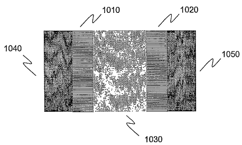
[00110] FIG. 10 is a schematic illustration of a m-i-n LED 1000 based on a
parallel array of GaN nanowires that can be developed using any of methods
200, 700 or 800. LED 1000 includes dense thin film of nanowires 1010,
dense thin film of nanowires 1020, metal to insulator junction 1030, cathode
contact 1040 and cathode contact 1050.
[00111] Dense thin films of nanowires 1010 and 1020 are deposited on a
substrate using either method 400 or one of the alternative approaches
described above. Similarly, metal to insulator junction 1030 can be fabricated
based on the approach described with respect to step 240 above. Cathode
contacts 1040 and 1050 can be created using the approach described with
respect to method 250 above.
[00112) In an embodiment, thin film of nanowires 1010 and 1020 include n-
doped GaN nanowires. In the embodiment illustrated in FIG. 10, in order to
insure that contact is made to all nanowires, two cathode contacts - cathode
contacts 1040 and 1050 can be deposited. A contact to an anode (not shown)
also exists that is coupled to metal-insulator junction 1030. The light
emission
direction of m-i-n LED 1000 is toward the bottom of the substrate (not shown)
that the nanowires have been deposited on. As a result, a transparent
substrate
is needed.
[00113] In this configuration, the entire area of nanowires, represented by
thin
film of nanowires 1010 and 1020 will emit light. When the nanowires are
closely packed, the light emission intensity per device area of m-i-n LED 1000
dramatically exceeds that of similar planar devices given the approximately
six times greater surface area around the individual nanowires relative to a
planar surface. The output of m-i-n LED 1000 will also have a high efficiency
because of the high crystalline quality of the nanowires.
[00114] FIG. 11 is a schematic illustration of a parallel lighting rod LED
1100
based on core-shell p-n junction nanowires, according to an embodiment of
the invention. LED 1100 includes p-GaN nanowire cores, such as p-GaN
nanowire core 1110, n-GaN nanowire shells, such as n-GaN nanowire core
1120, anode 1130 and cathode 1140. p-GaN nanowire cores, such as p-GaN
nanowire core 1110, have been exposed by etching away n-GaN nanowire
CA 02609042 2007-11-19
WO 2006/130359 PCT/US2006/019402
-30-
shells, such as n-GaN nanowire shell 1120, for making an ohmic contact to it.
Anode 1130 is coupled to p-GaN nanowire cores, such as p-GaN nanowire
core 1110. Cathode 1140 is coupled to n-GaN nanowire shells, such as n-GaN
nanowire shel11120. This configuration has very high efficiency.
Conclusion
[00115] While various embodiments of the present invention have been
described above, it should be understood that they have been presented by way
of example only, and not limitation. It will be apparent to persons skilled in
the relevant art that various changes in form and detail can be made therein
without departing from the spirit and scope of the invention. Thus, the
breadth
and scope of the present invention should not be limited by any of the above-
described exemplary embodiments, but should be defined only in accordance
with the following claims and their equivalents.