Note: Descriptions are shown in the official language in which they were submitted.
CA 02609614 2007-11-23
WO 2006/130665 PCT/US2006/021082
MICROELECTROMECHANICAL SYSTEMS (MEMS) DEVICE
INCLUDING A SUPERLATTICE AND ASSOCIATED METHODS
Field of the invention
[0001] The present invention relates to the field of
semiconductors, and, more particularly, to semiconductor
devices comprising superlattices and associated methods.
Background of the Invention
[0002] Structures and techniques have been proposed to
enhance the performance of semiconductor devices, such as
by enhancing the mobility of the charge carriers. For
example, U.S. Patent Application No. 2003/0057416 to
Currie et al. discloses strained material layers of
silicon, silicon-germanium, and relaxed silicon and also
including impurity-free zones that would otherwise cause
performance degradation. The resulting biaxial strain in
the upper silicon layer alters the carrier mobilities
enabling higher speed and/or lower power devices.
Published U.S. Patent Application No. 2003/0034529 to
Fitzgerald et al. discloses a CMOS inverter also based
upon similar strained silicon technology.
CA 02609614 2007-11-23
WO 2006/130665 PCT/US2006/021082
[0003] U.S. Patent No. 6,472,685 B2 to Takagi
discloses a semiconductor device including a silicon and
carbon layer sandwiched between silicon layers so that
the conduction band and valence band of the second
silicon layer receive a tensile strain. Electrons having
a smaller effective mass, and which have been induced by
an electric field applied to the gate electrode, are
confined in the second silicon layer, thus, an n-channel
MOSFET is asserted to have a higher mobility.
[0004] U.S. Patent No. 4,937,204 to Ishibashi et al.
discloses a superlattice in which a plurality of layers,
less than eight monolayers, and containing a fractional
or binary or a binary compound semiconductor layer, are
alternately and epitaxially grown. The direction of main
current flow is perpendicular to the layers of the
superlattice.
C0005] U.S. Patent No. 5,357,119 to Wang et al.
discloses a Si-Ge short period superlattice with higher
mobility achieved by reducing alloy scattering in the
superlattice. Along these lines, U.S. Patent No.
5,683,934 to Candelaria discloses an enhanced mobility
MOSFET including a channel layer comprising an alloy of
silicon and a second material substitutionally present in
the silicon lattice at a percentage that places the
channel layer under tensile stress.
[0006] U.S. Patent No. 5,216,262 to Tsu discloses a
quantum well structure comprising two barrier regions and
a thin epitaxially grown semiconductor layer sandwiched
between the barriers. Each barrier region consists of
alternate layers of Si02/Si with a thickness generally in
a range of two to six monolayers. A much thicker section
of silicon is sandwiched between the barriers.
2
CA 02609614 2007-11-23
WO 2006/130665 PCT/US2006/021082
[0007] An article entitled "Phenomena in silicon
nanostructure devices" also to Tsu and published online
September 6, 2000 by Applied Physics and Materials
Science & Processing, pp. 391-402 discloses a
semiconductor-atomic superlattice (SAS) of silicon and
oxygen. The Si/O superlattice is disclosed as useful in a
silicon quantum and light-emitting devices. In
particular, a green electromuminescence diode structure
was constructed and tested. Current flow in the diode
structure is vertical, that is, perpendicular to the
layers of the SAS. The disclosed SAS may include
semiconductor layers separated by adsorbed species such
as oxygen atoms, and CO molecules. The silicon growth
beyond the adsorbed monolayer of oxygen is described as
epitaxial with a fairly low defect density. One SAS
structure included a 1.1 nm thick silicon portion that is
about eight atomic layers of silicon, and another
structure had twice this thickness of silicon. An article
to Luo et al. entitled "Chemical Design of Direct-Gap
Light-Emitting Silicon" published in Physical Review
Letters, Vol. 89, No. 7 (August 12, 2002) further
discusses the light emitting SAS structures of Tsu.
[0008] Published International Application WO
02/103,767 Al to Wang, Tsu and Lofgren, discloses a
barrier building block of thin silicon and oxygen,
carbon, nitrogen, phosphorous, antimony, arsenic or
hydrogen to thereby reduce current flowing vertically
through the lattice more than four orders of magnitude.
The insulating layer/barrier layer allows for low defect
epitaxial silicon to be deposited next to the insulating
layer.
3
CA 02609614 2007-11-23
WO 2006/130665 PCT/US2006/021082
[0009] Published Great Britain Patent Application
2,347,520 to Mears et al. discloses that principles of
Aperiodic Photonic Band-Gap (APBG) structures may be
adapted for electronic bandgap engineering. In
particular, the application discloses that material
parameters, for example, the location of band minima,
effective mass, etc, can be tailored to yield new
aperiodic materials with desirable band-structure
characteristics. Other parameters, such as electrical
conductivity, thermal conductivity and dielectric
permittivity or magnetic permeability are disclosed as
also possible to be designed into the material.
Summary of the Invention
[0010] A microelectromechanical system (MEMS) device
may include a substrate and at least one movable member
supported by the substrate. Furthermore, the at least one
movable member may include a superlattice including a
plurality of stacked groups of layers with each group of
layers of the superlattice comprising a plurality of
stacked base semiconductor monolayers defining a base
semiconductor portion, and at least one non-semiconductor
monolayer constrained within a crystal lattice of
adjacent base semiconductor portions.
[0011] More particularly, the superlattice may be a
piezoelectric superlattice. The MEMS device may further
include a driver carried by the substrate for driving the
at least one movable member. Also, a first electrically
conductive contact may be carried by the at least one
movable member, and a second electrically conductive
contact may be carried by the substrate and aligned with
the first electrically conductive contact.
4
CA 02609614 2007-11-23
WO 2006/130665 PCT/US2006/021082
[0012] The MEMS device may further include a first
radio frequency (RF) signal line connected to the first
electrically conductive contact, and a second RF signal
line connected to the second electrically conductive
contact. In addition, a pair of bias voltage contacts may
be included for applying a bias voltage to the
superlattice for moving the at least one movable member.
Furthermore, portions of the superlattice may be spaced
apart from the substrate. Also, the MEMS device may
further include a dielectric anchor carried by the
substrate, and the at least one movable member may be
supported by the dielectric anchor.
[0013] With respect to the superlattice, the base
semiconductor may include silicon, and the at least one
non-semiconductor monolayer may include oxygen, for
example. More particularly, the at least one non-
semiconductor monolayer may include a non-semiconductor
selected from the group consisting essentially of oxygen,
nitrogen, fluorine, and carbon-oxygen. Further, at least
one non-semiconductor monolayer may be a single monolayer
thick. All of the base semiconductor portions may be a
same number of monolayers thick, or at least some of the
base semiconductor portions may be a different number of
monolayers thick. Additionally, opposing base
semiconductor portions in adjacent groups of layers of
the at least one superlattice may be chemically bound
together.
[0014] A method aspect is for making a MEMS device and
may include providing a substrate, and forming at least
one movable member supported by the substrate. The at
least one movable member may comprise a superlattice
including a plurality of stacked groups of layers with
CA 02609614 2007-11-23
WO 2006/130665 PCT/US2006/021082
each group of layers of the superlattice comprising a
plurality of stacked base semiconductor monolayers
defining a base semiconductor portion and at least one
non-semiconductor monolayer constrained within a crystal
lattice of adjacent base semiconductor portions.
Brief Description of the Drawings
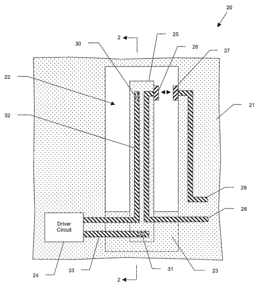
(0015] FIG. 1 is a top view of a
microelectromechanical system (MEMS) device in accordance
with the present invention including a superlattice.
[0016] FIG. 2 is cross-sectional view of the MEMS
device of FIG. 1 taken along line 2-2.
(0017] FIG. 3 is a greatly enlarged schematic cross-
sectional view of the superlattice as shown in FIG. 1.
[0018] FIG. 4 is a perspective schematic atomic
diagram of a portion of the superlattice shown in FIG. 3.
[00191 FIG. 5 is a greatly enlarged schematic cross-
sectional view of another embodiment of a superlattice
that may be used in the device of FIG. 1.
(0020] FIG. 6A is a graph of the calculated band
structure from the gamma point (G) for both bulk silicon
as in the prior art, and for the 4/1 Si/O superlattice as
shown in FIG. 2.
[0021] FIG. 6B is a graph of the calculated band
structure from the Z point for both bulk silicon as in
the prior art, and for the 4/1 Si/O superlattice as shown
in FIGS. 1.
[0022] FIG. 6C is a graph of the calculated band
structure from both the gamma and Z points for both bulk
silicon as in the prior art, and for the 5/1/3/1 Si/O
superlattice as shown in FIG. 5.
6
CA 02609614 2007-11-23
WO 2006/130665 PCT/US2006/021082
[0023] FIGS. 7A-7F are a series of cross-sectional
views illustrating a method for making superlattices for
use in a MEMS device in accordance with the invention.
[0024] FIGS. 8A-8F are a series of cross-sectional
views illustrating another method for making
superlattices for use in a MEMS device in accordance with
the invention.
[00251 FIGS. 9A-9F are a series of cross-sectional
views illustrating still another method for making
superlattices for use in a MEMS device in accordance with
the invention.
[00261 FIGS. 10A-10G are a series of cross-sectional
views illustrating yet another method for making
superlattices for use in a MEMS device in accordance with
the invention.
[0027] FIGS. 11A-11F are a series of cross-sectional
views illustrating another method for making
superlattices for use in a MEMS device in accordance with
the invention.
[0028] FIGS. 12A-12G are a series of cross-sectional
views illustrating still another method for making
superlattices for use in a MEMS device in accordance with
the invention.
Detailed Description of the Preferred Embodiments
[0029] The present invention will now be described
more fully hereinafter with reference to the accompanying
drawings, in which preferred embodiments of the invention
are shown. This invention may, however, be embodied in
many different forms and should not be construed as
limited to the embodiments set forth herein. Rather,
these embodiments are provided so that this disclosure
will be thorough and complete, and will fully convey the
7
CA 02609614 2007-11-23
WO 2006/130665 PCT/US2006/021082
scope of the invention to those skilled in the art. Like
numbers refer to like elements throughout, and prime
notation is used to indicate similar elements in
alternate embodiments.
[0030] The present invention relates to controlling
the properties of semiconductor materials at the atomic
or molecular level to achieve improved performance within
semiconductor devices. Further, the invention relates to
the identification, creation, and use of improved
materials for use in the conduction paths of
semiconductor devices.
[0031] Applicants theorize, without wishing to be
bound thereto, that certain superlattices as described
herein reduce the effective mass of charge carriers and
that this thereby leads to higher charge carrier
mobility. Effective mass is described with various
definitions in the literature. As a measure of the
improvement in effective mass Applicants use a
"conductivity reciprocal effective mass tensor", Me' and
M_' for electrons and holes respectively, defined as:
E f(Vk E(k, n)); (Vk E(k, n)); a.f (E(k, naE), EF, T ) dsk
M VL (E T)~ E> EF B.Z.
e,tJ F ~ I f .f(E(k,n),EF,T)d3k
E>Er B.Z.
for electrons and:
-Y f(0kE(k,n))i (VkE(k,n)),/ ~ af (E(k, ii), EF , T ) d 3k
aE
M-1(E T) - E<Er= B,Z.
h,ij F ~
E (1-.f(E(k,n),EF,T))d3k
E<EF B.Z.
for holes, where f is the Fermi-Dirac distribution, EF is
the Fermi energy, T is the temperature (Kelvin), E(k,n)
8
CA 02609614 2007-11-23
WO 2006/130665 PCT/US2006/021082
is the energy of an electron in the state corresponding
to wave vector k and the nth energy band, the indices i
and j refer to Cartesian coordinates x, y and z, the
integrals are taken over the Brillouin zone (B.Z.), and
the summations are taken over bands with energies above
and below the Fermi energy for electrons and holes
respectively.
[0032] Applicants' definition of the conductivity
reciprocal effective mass tensor is such that a tensorial
component of the conductivity of the material is greater
for greater values of the corresponding component of the
conductivity reciprocal effective mass tensor. Again
Applicants theorize without wishing to be bound thereto
that the superlattices described herein set the values of
the conductivity reciprocal effective mass tensor so as
to enhance the conductive properties of the material,
such as typically for a preferred direction of charge
carrier transport. The inverse of the appropriate tensor
element is referred to as the conductivity effective
mass. In other words, to characterize semiconductor
material structures, the conductivity effective mass for
electrons/holes as described above and calculated in the
direction of intended carrier transport is used to
distinguish improved materials.
[0033] Using the above-described measures, one can
select materials having improved band structures for
specific purposes. One such example would be a
superlattice 25 material (which will be discussed in
further detail below) used in a microelectromechanical
system (MEMS) device 20. Certain applications have
developed wherein relatively small devices such as
tunable capacitors, switches, etc. are desirably used.
9
CA 02609614 2007-11-23
WO 2006/130665 PCT/US2006/021082
Such devices may advantageously be made using MEMS
manufacturing processes in which very small movable
components are formed on a substrate using a combination
of deposition, plating or other additive processes, and
selective etching, and/or other lift-off techniques.
[0034] Such techniques typically form a structure
which is ultimately partially released or suspended to
permit mechanical motion, typically as a result of an
electrostatic force. The electrostatic force may be
generated by applying an electrical voltage to spaced-
apart conductors. One common MEMS structure is a switch
provided by a conductive beam anchored at one end and
with an opposite end that can be brought into engagement
with an adjacent contact via an applied electrostatic
force.
[0035] An article by Los Santo et al. entitled "RF
MEMS for Ubiquitous Wireless Connectivity: Part 1-
Fabrication," IEEE Microwave Magazine, December 2004,
discusses various applications for MEMS devices, and is
hereby incorporate herein by reference in its entirety.
This article states that MEMS technology may be applied
to radio-frequency (RF)/microwave systems, as RF MEMS may
provide passive devices such as switches, switchable
(two-state) capacitors, tunable capacitors (varactors),
inductors, transmission lines and resonators. As such,
these devices may be used in wireless appliances
operating in the home/ground, mobile, and space spheres,
such as handsets, base stations, and satellites.
[0036] An exemplary MEMS device 20 (i.e., a switch)
including the superlattice 25 is first described with
reference to FIGS. 1 and 2. It should be noted that while
a preferred embodiment of a MEMS switch is described
CA 02609614 2007-11-23
WO 2006/130665 PCT/US2006/021082
herein, the superlattice 25 may advantageously be used in
numerous types of MEMS devices, including those mentioned
above, as will be appreciated by those skilled in the art
based upon the disclosure set forth herein.
[0037] As described in the Los Santos et al. article,
one of the physical bases for actuating a MEMS is the
inverse piezoelectric effect. When a voltage is applied
across a piezoelectric layer, it causes a mechanical
deformation of the layer. The resulting deformation can
open a closed relay or close an open relay. The
conventional approach to the manufacture of MEMS switches
is to form a relay using a cantilever structure. Though
such structures provide the desired functionality, their
fabrication can be difficult.
[0038] In the MEMS device 20, the superlattice 25 is
electrically polled to be piezoelectric and provide a
movable member for the MEMS device, as discussed above.
In particular, the MEMS device 20 further illustratively
includes a substrate 21, such as a semiconductor
substrate (e.g., silicon, SOZ, etc.). A trench 22 is
formed in the substrate 21 around and underneath the
superlattice 25 so that portions of the superlattice are
spaced apart from the substrate (i.e., the underside
thereof), and a dielectric anchor 23 anchors the
superlattice to the substrate above the bottom of the
trench as shown. Of course, other arrangements may also
be used, as will be appreciated by those skilled in the
art.
I0039] The MEMS device 20 further illustratively
includes a driver circuit 24 carried by the substrate 21
for driving the superlattice 25, i.e., the movable
member. In the illustrated MEMS switch embodiment, a
11
CA 02609614 2007-11-23
WO 2006/130665 PCT/US2006/021082
first electrically conductive contact 26 is
illustratively carried by the movable member, and a
second electrically conductive contact 27 is
illustratively carried by the substrate 21 and aligned
with the first electrically conductive contact as shown
(FIG. 1). In addition, a first signal line 28, such as an
RF signal line, for example, is connected to the first
electrically conductive contact 26, and a second signal
line 29 (which may also be an RF signal line) is
illustratively connected to the second electrically
conductive contact 27.
[0040] A pair of bias voltage contacts 30, 31 are
coupled to the superlat-tice 25 for applying a bias
voltage thereto for moving the movable member. In
particular, the bias voltage contacts 30, 31 may be
electrically conductive vias formed in the superlattice
25 as shown, although surface contacts or metallizations
may also be used in some embodiments. Electrically
conductive traces/metallizations 32, 33 respectively
connect the bias voltage contacts 30, 31 to positive and
negative connectors of the driver circuit 24. As such,
when the driver circuit 24 applies a bias voltage to the
superlattice 25 via the bias voltage contacts 30, 31,
this causes a mechanical deformation of the superlattice,
which in turn causes the movable member to move the first
electrical contact 26 toward the second electrical
contact 27, as shown by the two-headed arrow in FIG. 1.
This advantageously closes the switch and allows a signal
(e.g., an RF signal) to be conducted between the first
and second signal lines 28, 29. Moreover, when the bias
voltage is removed, the movable member moves the first
contact 26 away from the second contact 27 so that the
12
CA 02609614 2007-11-23
WO 2006/130665 PCT/US2006/021082
switch is opened, as will be appreciated by those skilled
in the art.
[0041] An oxide layer 34 (FIG. 2) is formed over the
entire superlattice semiconductor region, and is
preferentially removed where contact to the superlattice
material is desired. It should be noted that in the
illustrated embodiment the trench 22 and sides/bottom of
the movable member are shown as being unpassivated.
However, it is possible to form a dielectric layer, such
as Si02, on the exposed semiconductor material if desired
in some embodiments, as will be appreciated by those
skilled in the art.
[0042] Referring now additionally to FIGS. 3 and 4,
the superlattice 25 has a structure that is controlled at
the atomic or molecular level and may be formed using
known techniques of atomic or molecular layer deposition.
The superlattice 25 includes a plurality of layer groups
45a-45n arranged in stacked relation, as noted above, as
perhaps best understood with specific reference to the
schematic cross-sectional view of FIG. 3.
[0043] Each group of layers 45a-45n of the
superlattice 25 illustratively includes a plurality of
stacked base semiconductor monolayers 46 defining a
respective base semiconductor portion 46a-46n and an
energy band-modifying layer 50 thereon. The energy band-
modifying layers 50 are indicated by stippling in FIG. 3
for clarity of illustration.
[0044] The energy-band modifying layer 50
illustratively includes one non-semiconductor monolayer
constrained within a crystal lattice of adjacent base
semiconductor portions. That is, opposing base
semiconductor monolayers 46 in adjacent groups of layers
13
CA 02609614 2007-11-23
WO 2006/130665 PCT/US2006/021082
45a-45n are chemically bound together. For example, in
the case of silicon monolayers 46, some of the silicon
atoms in the upper or top semiconductor monolayer of the
group of monolayers 46a will be covalently bonded with
silicon atoms in the lower or bottom monolayer of the
group 46b. This allows the crystal lattice to continue
through the groups of layers despite the presence of the
non-semiconductor monolayer(s) (e.g., oxygen
monolayer(s)). Of course, there will not be a complete or
pure covalent bond between the opposing silicon layers 46
of adjacent groups 45a-45n as some of the silicon atoms
in each of these layers will be bonded to non-
semiconductor atoms (i.e., oxygen in the present
example), as will be appreciated by those skilled in the
art.
[0045] In other embodiments, more than one non-
semiconductor layer monolayer may be possible. By way of
example, the number of non-semiconductor monolayers in
the energy band-modifying layer 50 may preferably be less
than about five monolayers to thereby provide desired
energy band-modifying properties.
[0046] It should be noted that reference herein to a
non-semiconductor or semiconductor monolayer means that
the material used for the monolayer would be a non-
semiconductor or semiconductor if formed in bulk. That
is, a single monolayer of a material, such as
semiconductor, may not necessarily exhibit the same
properties that it would if formed in bulk or in a
relatively thick layer, as will be appreciated by those
skilled in the art.
[0047] Applicants theorize without wishing to be bound
thereto that energy band-modifying layers 50 and adjacent
14
CA 02609614 2007-11-23
WO 2006/130665 PCT/US2006/021082
base semiconductor portions 46a-46n cause the
superlattice 25 to have a lower appropriate conductivity
effective mass for the charge carriers in the parallel
layer direction than would otherwise be present.
Considered another way, this parallel direction is
orthogonal to the stacking direction. The band modifying
layers 50 may also cause the superlattice 25 to have a
common energy band structure, while also advantageously
functioning as an insulator between layers or regions
vertically above and below the superlattice. Moreover,
this structure also advantageously provides a barrier to
dopant andjor material bleed or diffusion between layers
vertically above and below the superlattice 25. In
addition, it is theorized without wishing to be bound
thereto that the superlattice 25 may be electrically
polled so that it is piezoelectric, as will be
appreciated by those skilled i.n the art.
[0048] It is also theorized that the superlattice 25
provides a higher charge carrier mobility based upon the
lower conductivity effective mass than would otherwise be
present. Of course, all of the above-described properties
of the superlattice 25 need not be utilized in every
application. For example, in some applications the
superlattice 25 may only be used for its dopant
blocking/insulation properties or its enhanced mobility,
or it may be used for both in other applications, as will
be appreciated by those skilled in the art.
[0049] A cap layer 52 is on an upper layer group 45n
of the superlattice 25. The cap layer 52 may comprise a
plurality of base semiconductor monolayers 46. The cap
layer 52 may have between 2 to 100 monolayers of the base
CA 02609614 2007-11-23
WO 2006/130665 PCT/US2006/021082
semiconductor, and, more preferably between 10 to 50
monolayers. Other thicknesses may be used as well.
[0050] Each base semiconductor portion 46a-46n may
comprise a base semiconductor selected from the group
consisting of Group IV semiconductors, Group III-V
semiconductors, and Group II-VI semiconductors. Of
course, the term Group IV semiconductors also includes
Group IV-IV semiconductors, as will be appreciated by
those skilled in the art. More particularly, the base
semiconductor may comprise at least one of silicon and
germanium, for example.
[0051] Each energy band-modifying layer 50 may
comprise a non-semiconductor selected from the group
consisting of oxygen, nitrogen, fluorine, and carbon-
oxygen, for example. The non-semiconductor is also
desirably thermally stable through deposition of a next
layer to thereby facilitate manufacturing. In other
embodiments, the non-semiconductor may be another
inorganic or organic element or compound that is
compatible-with the given semiconductor processing, as
will be appreciated by those skilled in the art.
[0052] It should be noted that the term "monolayer" is
meant to include a single atomic layer and also a single
molecular layer. It is also noted that the energy band-
modifying layer 50 provided by a single monolayer is also
meant to include a monolayer wherein not all of the
possible sites are occupied. For example, with particular
reference to the atomic diagram of FIG. 3, a 4/1
repeating structure is illustrated for silicon as the
base semiconductor material, and oxygen as the energy
band-modifying material. Only half of the possible sites
for oxygen are occupied.
16
CA 02609614 2007-11-23
WO 2006/130665 PCT/US2006/021082
[0053] In other embodiments and/or with different
materials this one half occupation would not necessarily
be the case as will be appreciated by those skilled in
the art. Indeed it can be seen even in this schematic
diagram, that individual atoms of oxygen in a given
monolayer are not precisely aligned along a flat plane as
will also be appreciated by those of skill in the art of
atomic deposition. By way of example, a preferred
occupation range is from about one-eighth to one-half of
the possible oxygen sites being full, although other
numbers may be used in certain embodiments.
[0054] Silicon and oxygen are currently widely used in
conventional semiconductor processing, and, hence,
manufacturers will be readily able to use these materials
as described herein. Atomic or monolayer deposition is
also now widely used. Accordingly, semiconductor devices
incorporating the superlattice 25 in accordance with the
invention may be readily adopted and implemented, as will
be appreciated by those skilled in the art.
[0055] It is theorized without wishing to be bound
thereto, that for a superlattice, such as the Si/O
superlattice, for example, that the number of silicon
monolayers should desirably be seven or less so that the
energy band of the superlattice is common or relatively
uniform throughout to achieve the desired advantages. The
4/1 repeating structure shown in FIG. 3, for Si/O has
been modeled to indicate an enhanced mobility for
electrons and holes in the X direction. For example, the
calculated conductivity effective mass for electrons
(isotropic for bulk silicon) is 0.26 and for the 4/1 SiO
superlattice in the X direction it is 0.12 resulting in a
ratio of 0.46. Similarly, the calculation for holes
17
CA 02609614 2007-11-23
WO 2006/130665 PCT/US2006/021082
yields values of 0.36 for bulk silicon and 0.16 for the
4/1 Si/O superlattice resulting in a ratio of 0.44.
[0056] While such a directionally preferential feature
may be desired in certain semiconductor devices, other
devices may benefit from a more uniform increase in
mobility in any direction parallel to the groups of
layers. It may also be beneficial to have an increased
mobility for both electrons and holes, or just one of
these types of charge carriers, as will be appreciated by
those skilled in the art.
[0057] The lower conductivity effective mass for the
4/1 Si/O embodiment of the superlattice 25 may be less
than two-thirds the conductivity effective mass than
would otherwise occur, and this applies for both
electrons and holes. It may be appropriate to dope the
superlattice 25 as well. It should be noted, however,
that one or more groups of layers 45 of the superlattice
25 may remain substantially undoped depending upon the
particular type of MEMS device that is being implemented
as well as the position of the superlattice within the
device, as will be appreciated by those skilled in the
art.
[0058] Referring now additionally to FIG. 5, another
embodiment of a superlattice 25' in accordance with the
invention having different properties is now described.
In this embodiment, a repeating pattern of 3/1/5/1 is
illustrated. More particularly, the lowest base
semiconductor portion 46a' has three monolayers, and the
second lowest base semiconductor portion 46b' has five
monolayers. This pattern repeats throughout the
superlattice 25'. The energy band-modifying layers 50'
may each include a single monolayer. For such a
18
CA 02609614 2007-11-23
WO 2006/130665 PCT/US2006/021082
superlattice 25' including Si/0, the enhancement of
charge carrier mobility is independent of orientation in
the plane of the layers. Those other elements of FIG. 5
not specifically mentioned are similar to those discussed
above with reference to FIG. 3 and need no further
discussion herein.
[0059] In some device embodiments, all of the base
semiconductor portions 46a-46n of a superlattice 25 may
be a same number of monolayers thick. In other
embodiments, at least some of the base semiconductor
portions 46a-46n may be a different number of monolayers
thick. In still other embodiments, all of the base
semiconductor portions 46a-46n may be a different number
of monolayers thick.
[0060] In FIGS. 6A-6C band structures calculated using
Density Functional Theory (DFT) are presented. It is well
known in the art that DFT underestimates the absolute
value of the bandgap. Hence all bands above the gap may
be shifted by an appropriate "scissors correction."
However the shape of the band is known to be much more
reliable. The vertical energy axes should be interpreted
in this light.
[0061] FIG. 6A shows the calculated band structure
from the gamma point (G) for both bulk silicon
(represented by continuous lines) and for the 4/1 Si/O
superlattice 25 as shown in FIG. 3 (represented by dotted
lines). The directions refer to the unit cell of the 4/1
Si/O structure and not to the conventional unit cell of
Si, although the (001) direction in the figure does
correspond to the (001) direction of the conventional
unit cell of Si, and, hence, shows the expected location
of the Si conduction band minimum. The (100) and (010)
19
CA 02609614 2007-11-23
WO 2006/130665 PCT/US2006/021082
directions in the figure correspond to the (110) and (-
110) directions of the conventional Si unit cell. Those
skilled in the art will appreciate that the bands of Si
on the figure are folded to represent them on the
appropriate reciprocal lattice directions for the 4/1
Si/O structure.
[0062] It can be seen that the conduction band minimum
for the 4/1 Si/O structure is located at the gamma point
in contrast to bulk silicon (Si), whereas the valence
band minimum occurs at the edge of the Brillouin zone in
the (001) direction which we refer to as the Z point. One
may also note the greater curvature of the conduction
band minimum for the 4/1 Si/O structure compared to the
curvature of the conduction band minimum for Si owing to
the band splitting due to the perturbation introduced by
the additional oxygen layer.
[0063] FIG. 6B shows the calculated band structure
from the Z point for both bulk silicon (continuous lines)
and for the 4/1 Si/O superlattice 25 (dotted lines) of
FIG. 3. This figure illustrates the enhanced curvature of
the valence band in the (100) direction.
[0064] FIG. 6C shows the calculated band structure
from both the gamma and Z point for both bulk silicon
(continuous lines) and for the 5/1/3/1 Si/O structure of
the superlattice 25' of FIG. 5 (dotted lines). Due to the
symmetry of the 5/1/3/1 Si/O structure, the calculated
band structures in the (100) and (010) directions are
equivalent. Thus the conductivity effective mass and
mobility are expected to be isotropic in the plane
parallel to the layers, i.e., perpendicular to the (001)
stacking direction. Note that in the 5/1/3/1 Si/O example
CA 02609614 2007-11-23
WO 2006/130665 PCT/US2006/021082
the conduction band minimum and the valence band maximum
are both at or close to the Z point.
[0065] Although increased curvature is an indication
of reduced effective mass, the appropriate comparison and
discrimination may be made via the conductivity
reciprocal effective mass tensor calculation. This leads
Applicants to further theorize that the 5/1/3/1
superlattice 25' should be substantially direct bandgap.
As will be understood by those skilled in the art, the
appropriate matrix element for optical transition is
another indicator of the distinction between direct and
indirect bandgap behavior.
[0066] Applicant theorizes without wishing to be bound
thereto that modifications to the lattice discussed in
the above paragraphs produce a superlattice semiconductor
material that has piezoelectric properties, unlike
silicon, which is not piezoelectric.
[0067] Various process flows for forming the
superlattice 25 for use in MEMS devices will now be
described. Generally speaking, the MEMS device 20 is
fabricated by forming a piezoelectric region or film
comprising the superlattice 25 along the sidewalls of a
trench. After the film is formed and metallized, it is
etched free of mechanical support (i.e., the trench 22
thereunder) except for one end, which in the embodiment
illustrated in FIGS. 1 and 2 is carried by the dielectric
anchor 23.
[0068] Turning to FIGS. 7A-7F, a first process flow is
now described. This process sequence uses deposition
steps to fill an etched trench 70 in a silicon-on-
insulator (SOI) substrate. More particularly, the SOI
substrate includes a dielectric (e.g., Si02) layer 71 and
21
CA 02609614 2007-11-23
WO 2006/130665 PCT/US2006/021082
a semiconductor (e.g., silicon) layer 72 on the
dielectric layer. A pad oxide layer 73 is formed on the
semiconductor layer 72, after which a nitride (e.g.,
silicon nitride) layer 74 is deposited thereon, and
photomasking and etch steps are performed to form the
trench 70.
[0069] Next, a superlattice 75 (such as those
described above) is selectively deposited on the walls of
the trench 70. A dielectric 76, dielectric sandwich, or
other trench fill material is then deposited over the
superlattice 75 and the nitride layer 74, followed by a
planarization step (FIG. 7D) that removes all material
above the nitride layer. The nitride layer 74 and pad
oxide layer 73 are then removed by etching, followed by
the semiconductor layer 72. The material used to fill the
trench 70 (i.e., the dielectric 76) is then etched, at
which point the substrate is ready for oxidation, contact
formation, metallization, and release etching to form the
above-described MEMS device 20 (or other MEMS devices).
[0070] Yet another flow process which similarly uses
deposition steps to fill an etched trench is now
described with reference to FIGS. 8A-8F. It should be
noted that in these and the following series of flow
diagrams discussed below, similar elements are indicated
by increments of ten (e.g., the dielectric layer 71 is
similar to the dielectric layer 81, 91, etc.). As such,
these elements are only described upon the first
occurrence thereof.
[0071] The process illustrated in FIGS. 8A-8F is
similar to the above-described approach of FIGS. 7A-7F,
except that during the superlattice 85 deposition single
crystal superlattice semiconductor material is formed on
22
CA 02609614 2007-11-23
WO 2006/130665 PCT/US2006/021082
the trench 80 walls, while polycrystalline superlattice
semiconductor material 87 (which is shown with stippling
for clarity of illustration) is formed on the trench
bottom and the nitride layer 84. After trench filling and
planarization steps (FIGS. 8C and 8D), portions of the
polycrystalline silicon 87 are etched away, and the
remainder thereof is oxidized to form an oxide layer 88
(FIG. 8E). The nitride layer 84 and pad oxide layer 83
are removed (i.e., etched). The substrate is then ready
for contact formation, metallization and a release etch,
as discussed above (FIG. 8F).
[00721 Four process flows that may be used to form a
separate lateral piezoelectric cantilever superlattice
structure along each sidewall of a trench are now
described with reference to FIGS. 9-12. More
particularly, the process illustrated in FIGS. 9A-9F is
similar to the process illustrated in FIGS 7A-7F, with
the exception that the superlattice 95 is selectively
deposited on the trench walls 90, as opposed to filling
the entire trench.
[00731 Still another process similar to the one
illustrated in FIGS. 9A-9F is illustrated in FIGS. 10A-
10F. This process begins with a standard semiconductor
substrate 102, as opposed to an SOI substrate. The other
difference is that an oxide layer (e.g., Si02) is formed
in the bottom of the trench 100 prior to selective
deposition of the superlattice 105 on the sidewalls of
the trench (FIG. 10B). Another process illustrated in
FIGS. 11A-11F is similar to the process illustrated in
FIGS. 8A-8F, with the exception that the superlattice 115
is selectively deposited on the sidewalls of the trench
110, as opposed to filling the entire trench. Yet another
23
CA 02609614 2007-11-23
WO 2006/130665 PCT/US2006/021082
process illustrated in FIGS. 12A-12G is similar to the
process illustrated in FIGS. 10A-10G, with the exception
that it incorporates polysilicon deposition as described
above with reference to FIGS. 8A-8F. In all of the
process sequences shown in FIGS. 9-12, a layer of silicon
dioxide is present on top of the piezoelectric
superlattice material before contact opening are formed.
[0074] Many modifications and other embodiments will
come to the mind of one skilled in the art having the
benefit of the teachings presented in the foregoing
descriptions and the associated drawings. Therefore, it
is understood that such modifications and embodiments are
intended to be included within the scope of the appended
claims.
24