Note: Descriptions are shown in the official language in which they were submitted.
CA 02609646 2010-08-06
' WO 2006/132766
PCT/US2006/018790
1
LEAD FREE SOLAR CELL CONTACTS
FIELD OF THE INVENTION
This invention relates to lead- free and cadmium- free paste compositions
and a method of making contacts for solar cells as well as other related
components
used in fabricating photovoltaic cells.
BACKGROUND
Solar cells are generally made of semiconductor materials, such as silicon
(Si), which convert sunlight into useful electrical energy. Solar cells are,
in general,
made of thin wafers of Si in which the required PN junction is formed by
diffusing
phosphorus (P) from a suitable phosphorus source into a P-type Si wafer. The
side of
the silicon wafer on which sunlight is incident is generally coated with an
anti-
reflective coating (ARC) to prevent reflective loss of sunlight, which
increases the
solar cell efficiency. A two dimensional electrode grid pattern known as a
front
contact makes a connection to the N-side of silicon, and a coating of aluminum
(Al)
= makes connection to the P-side of the silicon (back contact). Further,
contacts known
as silver rear contacts, made out of silver or silver-aluminum paste are
printed and
fired on the N-side of silicon to enable soldering of tabs that electrically
connect one
cell to the next in a solar cell module. These contacts are the electrical
outlets from
the PN junction to the outside load.
Conventional pastes for solar cell contacts contain lead frits. Inclusion of
Pb0 in a glass component of a solar cell paste has the desirable effects of
(a) lowering
CA 02609646 2010-08-06
WO 2006/132766 PCT/US2006/018790
2
the firing temperature of paste compositions, (b) facilitating interaction
with the
silicon substrate and, upon firing, helping to form low resistance contacts
with silicon.
For these and other reasons Pb0 is a significant component in many
conventional
solar cell paste compositions. However, in light of environmental concerns,
the use of
Pb0 (as well as CdO), in paste compositions is now largely avoided whenever
possible. Hence a need exists in the photovoltaic industry for lead-free and
cadmium-
free paste compositions, which afford desirable properties using lead-free and
cadmium-free glasses in solar cell contact pastes.
SUMMARY OF THE INVENTION
The present invention provides lead-free and cadmium-free glass
compositions for use in solar cell contact paste materials that provide low
series
resistance (Rs) and high shunt resistance (Rsh) to give high performance solar
cells, as
measured by efficiency (1) and fill factor (FF). Generally, the present
invention
includes a solar cell comprising a contact, made from a mixture wherein, prior
to
firing, the mixture comprises a solids portion and an organics portion. The
solids
portion comprises from about 85 to about 99 wt% of a conductive metal
component
and from about 1 to about 15 wt% of a lead-free glass component.
The compositions and methods of the present invention overcome the
drawbacks of the prior art by optimizing interaction, bonding, and contact
formation
between contact components, typically silicon with either Ag (front contact)
or Al
(back contact) or Ag (silver rear contact), through the lead-free glass
medium. A
conductive paste containing glass and silver, or glass and aluminum, is
printed on a
silicon substrate, and fired to fuse the glass and sinter the metal therein.
For a silver
CA 02609646 2010-08-06
' WO 2006/132766
PCT/US2006/018790
3
rear contact, the metal component may comprise silver, or a combination of
silver and
aluminum powders and/or flakes. Upon firing, for a front contact, Ag/Si
conductive
islands are formed providing conductive bridges between bulk paste and silicon
wafer. In a front contact, the sequence and rates of reactions among glasses,
metals
and silicon, occurring as a function of temperature are factors in forming the
low
resistance contact between the silver paste and silicon wafer. The interface
structure
consists of multiple phases: substrate silicon, Ag/Si islands, Ag precipitates
within the
insulating glass layer, and bulk silver. The glass forms a nearly continuous
layer
between the silicon interface and the bulk silver. For a back contact, upon
firing, a p+
layer forms on the underlying silicon by liquid-phase epitaxy. This occurs
during the
resolidification of the aluminum-silicon (Al-Si) melt. High-bismuth lead-free
and
cadmium- free glasses allow low firing temperatures in making front contacts
owing
to their excellent flow characteristics relatively at low temperatures.
Relatively high-
silicon, low bismuth lead-free and cadmium- free glasses provide suitable
properties
for back contacts, without excessive interaction with backside Si. Similarly,
high-
bismuth lead-free and cadmium- free glasses allow the formation of suitable
lead-free
silver rear contacts on backside Si with optimal interaction with both Si and
back
contact Al layer.
The foregoing and other features of the invention are hereinafter more fully
described and particularly pointed out in the claims, the following
description setting
,=
forth in detail certain illustrative embodiments of the invention, these being
indicative, however, of but a few of the various ways in which the principles
of the
present invention may be employed.
CA 02609646 2010-08-06
3a
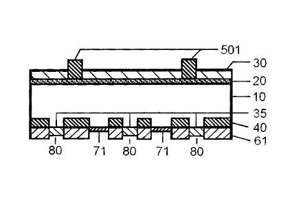
FIGS. 1A-1E provide a process flow diagram schematically illustrating the
fabrication of
a semiconductor device. Reference numerals shown in FIGS. 1A-1E are explained
below.
10: p-type silicon substrate
20: n-type diffusion layer
30: front side passivation layer/ anti-reflective coating (e.g., SiNX, Ti02,
Si02 film)
35: back side passivation layer (e.g., SiNX, Ti02, Si02 film)
40: p+ layer (back surface field, BSF)
60: aluminum paste formed on backside
61: aluminum back electrode after firing showing fire through of passivation
layer and
BSF formation
70: silver or silver/aluminum paste formed on backside
71: silver or silver/aluminum back electrode (obtained by firing back side
silver paste)
80: gap in silver aluminum back paste or electrode
500: silver paste formed on front side
501: silver front electrode after firing through ARC
CA 02609646 2010-08-06
) WO 2006/132766 PCT/US2006/018790
4
DETAILED DESCRIPTION OF THE INVENTION
Broadly, the invention provides a solar cell contact made from a mixture
wherein, prior to firing, the mixture comprises a solids portion and an
organics
portion, wherein the solids portion comprises from about 85 to about 99 wt%,
preferably about 88 to about 96 wt % of a conductive metal component, and from
about 1 to about 15 wt%, preferably about 2 to about 9 wt % and more
preferably
about 3 to about 8 wt % of a glass component, wherein the glass component is
lead-
free and cadmium- free. A solar panel comprising any solar cell herein is also
envisioned. When the solar cell contact is a front contact, the metal
component
preferably comprises silver, and the glass component comprises from about 5 to
about
85 mol% Bi203, and from about 1 to about 70 mol% Si02. The compositions used
in
making front contacts are also useful in making a busbar (silver rear contact)
for a
solar cell back contact. A silver (or silver-aluminum) rear contact in the
back makes
contact with both Si and the Al back contact layer, even though back contact
Al also
directly contacts Si. The silver rear contact in the back contact helps to
solder
connecting tabs to the solar cells that connect one cell to the next in a
solar cell
module. In a back contact, the metal component preferably comprises aluminum,
and
the glass component comprises from about 5 to about 55 mol% Bi203, from about
20
to about 70 mol% Si02, and from about 0.1 to about 35 mol% B203.
Broadly, silver- and glass-containing thick film pastes are used to make
front contacts for silicon-based solar cells to collect current generated by
exposure to
light. While the paste is generally applied by screen-printing, methods such
as
extrusion, pad printing, and hot melt printing may also be used. Solar cells
with
screen-printed front contacts are fired to relatively low temperatures (550 C
to 850 C
CA 02609646 2010-08-06
' WO 2006/132766
PCT/US2006/018790
wafer temperature; furnace set temperatures of 650 C to 1000 C) to form a low
resistance contact between the N-side of a phosphorus doped silicon wafer and
a
silver based paste. Methods for making solar cells are also envisioned herein.
Aluminum- and glass-containing back contacts are used to form low
resistance ohmic contacts on the back side of the solar cell due to large area
melting
and re solidification of Al doped (p+) epitaxially grown Si layer which
increases the
solar cell performance due to improved back surface field. For optimum
performance
a thick p+ re-grown region is believed to be ideal. It is also believed that
the rejection
of metallic impurities from the epitaxially growing p+ layer leads to high
carrier
lifetimes. These two factors are believed to increase the open circuit
voltage, and
more importantly, the open circuit voltage falls only slightly as the bulk
resistivity
increases. Therefore solar cell performance improves due to the formation of
substantial epitaxially re grown p+ layer in the Al back contact. Therefore
the
interaction of lead- free and cadmium- free glass in the back contact paste,
with Si
should be minimal, and its interaction with Al should be enough to form a
continuous
Al layer without beading.
Paste Glasses. The glass component of the pastes comprises, prior to
firing, one or more glass compositions. Each glass composition comprises oxide
fits
including, at a minimum, Bi203 and Si02. In particular, in various embodiments
of
the present invention, glass compositions for a front contact may be found in
Table 1.
Glass compositions for back contacts may be found in Table 2. More than one
glass
composition can be used, and compositions comprising amounts from different
columns in the same table are also envisioned. Regardless of the number of
glass
compositions used, the total content of 1Bi203 and SiO2 in the glass component
CA 02609646 2010-08-06
WO 2006/132766 PCT/US2006/018790
6
preferably falls within the range of about 5 to about 85 mol% Bi203 and from
about 1
to about 70 mol% Si02. If a second glass composition is used, the proportions
of the
glass compositions can be varied to control the extent of paste interaction
with silicon,
and hence the resultant solar cell properties. For example, within the glass
component, the first and second glass compositions may be present in a weight
ratio
of about 1:20 to about 20:1, and preferably about 1:3 to about 3:1. The glass
component preferably contains no lead or oxides of lead, and no cadmium or
oxides
of cadmium.
Table 1. Oxide fit ingredients for front contact glasses in mole percent.
Glass Composition I 11 111
Ingredient
Bi203 5-85 15-80 50-80
Si02 1-70 2-45 15-35
ZnO 0-55 0.1-25 1-15
V205 0-30 0.1-25 1-15
Table 2. Oxide fit ingredients for back contact glasses in mole percent.
Glass Composition IV V VI
Ingredient
Bi203 5-65 5-55 10-40
S102 15-70 20-70 30-65
B203 0-35 0.1-35 3-20
Alkali oxides 0-35 0.1-25 5-25
CA 02609646 2010-08-06
WO 2006/132766 PCT/US2006/018790
7
In addition to the oxides of Table 1 and Table 2, additional oxides may be
included in the glass component, for example about 1 to about 20 mol% of a
trivalent
oxide of one or more of Al, B, La, Y, Ga, In, Ce, and Cr; about 0.1 to about
15 mol%
of a tetravalent oxide of one or more of Ti, Zr and Hf; about 0.1 to about 20
mol% of
a pentavalent oxide of one or more of P, Ta, Nb, and Sb. Ag20 may be included
in
the silver paste glass as a source of silver, from about 0.1 to about 12 mol%.
Metal Component. In a solar cell contact, the metal must be conductive.
In a front contact, the metal component comprises silver. The source of the
silver can
be one or more fine powders of silver metal, or alloys of silver. A portion of
the
silver can be added as silver oxide (Ag20) or as silver salts such as silver
chloride
(AgC1), silver nitrate (AgNO3) or silver acetate (AgOOCCH3). The silver
particles
used in the paste may be spherical, flaked, or provided in a colloidal
suspension, and
combinations of the foregoing may be used. For example the solids portion of
the
paste may comprise about 80 to about 99 wt% spherical silver particles or
alternatively about 75 to about 90 wt% silver particles and about 1 to about
10 wt%
silver flakes. Alternatively the solids portion may comprise about 75 to about
90 wt%
silver flakes and about 1 to about 10 wt% of colloidal silver, or about 60 to
about 95
wt % of silver powder or silver flakes and about 0.1 to about 20 wt % of
colloidal
silver. Suitable commercial examples of silver particles are spherical silver
powder
Ag3000-1, silver flakes SF-29, and colloidal silver suspension RDAGCOLB, all
commercially available from Ferro Corporation, Cleveland, Ohio.
In a back contact, the metal component comprises aluminum or alloys of
aluminum. The aluminum metal component may come in any suitable form,
including those noted hereinabove for silver in the front contact.
CA 02609646 2010-08-06
WO 2006/132766 PCT/US2006/018790
8
For a silver rear contact, the metal component may comprise silver or a
combination of both silver and aluminum pastes as disclosed hereinabove.
Other Additives. Up to about 30wt % of other (i.e., inorganic) additives,
preferably up to about 25 wt % and more preferably up to about 20 wt%, may be
included as needed. Phosphorus can be added to the paste in a variety of ways
to
reduce the resistance of the front contacts. For example, certain glasses can
be
modified with P205 in the form of a powdered or fitted oxide, or phosphorus
can be
added to the paste by way of phosphate esters or other organo-phosphorus
compounds. More simply, phosphorus can be added as a coating to silver
particles
prior to making a paste. In such case, prior to pasting, the silver particles
are mixed
with liquid phosphorus and a solvent. For example, a blend of from about 85 to
about
95 wt % silver particles, from about 5 to about 15 wt % solvent and from about
0.5 to
about 10 wt % liquid phosphorus is mixed and the solvent evaporated.
Phosphorus
coated silver particles help ensure intimate mixing of phosphorus and silver
in the
inventive silver pastes.
Other additives such as fine silicon or carbon powder, or both, can be added
to control the reactivity of the metal component with silicon. For example
these fine
silicon or carbon powder can be added to the front contact silver paste to
control the
silver reduction and precipitation reaction. The silver precipitation at the
Ag/Si
interface or in the bulk glass, for the silver pastes in both front contacts
and silver rear
contacts, can also be controlled by adjusting the firing atmosphere (e.g.,
firing in
flowing N, or N2/H2/H20 mixtures). Fine particles of low melting metal
additives
(i.e., elemental metallic additives as distinct from metal oxides) such as Pb,
Bi, In, Ga,
Sn, and Zn and alloys of each with at least one other metal can be added to
provide a
CA 02609646 2010-08-06
WO 2006/132766 PCT/US2006/018790
9
contact at a lower temperature, or to widen the firing window. Zinc is the
preferred
metal additive, and a zinc-silver alloy is most preferred for the front
contact.
A mixture of (a) glasses or a mixture of (b) crystalline additives and glasses
or a mixture of (c) one or more crystalline additives can be used to formulate
a glass
component in the desired compositional range. The goal is to reduce the
contact
resistance and improve the solar cell electrical performance. For example,
second-
phase crystalline materials such as Bi203, Sb203, 1n203, Ga203, SnO, ZnO,
Si02,
Zr02, A1203, B203, V205, Ta205, various alumino-silicates, bismuth borates
such as
1213i203=Si02, 2Bi203=Si02, 3Bi203=5Si02 and Bi203.4Si02, bismuth silicates
such
as 6Bi203=Si02, Bi203 =
S102, 2Bi203=3Si02, bismuth titanates such as Bi203=2Ti02,
2Bi203.3TiO2, 2Bi203.4Ti02, and 6Bi203=Ti02, various vanadates such as
MgO .V205, SrO*V205, CaO=V205, BaO .V205, ZnO*V205, Na20 = 17V205,
K20=4V205, 2Li20=5V205, and bismuth vanadates such as 6Bi203=V205, BiVO4,
2Bi203=3V205, and BiV309, bismuth vanadium titanates such as
6.5Bi203=2.5V205=T102, zinc titanates such as 2Zn003Ti02, zinc silicates such
as
ZnO=Si02, zirconium silicates such as Zr02=Si02, and reaction products thereof
and
combinations thereof may be added to the glass component to adjust contact
properties. However, the total amounts of the above oxides must fall within
the
ranges specified for various embodiments disclosed elsewhere herein.
Organic Vehicle. The pastes herein include a vehicle or carrier which is
typically a solution of a resin dissolved in a solvent and, frequently, a
solvent solution
containing both resin and a thixotropic agent. The organics portion of the
pastes
comprises (a) at least about 80 wt % organic solvent; (b) up to about 15 wt %
of a
thermoplastic resin; (c) up to about 4 wt % of a thixotropic agent; and (d) up
to about
CA 02609646 2010-08-06
WO 2006/132766 PCT/US2006/018790
2 wt % of a wetting agent. The use of more than one solvent, resin,
thixotrope, and/or
wetting agent is also envisioned. Although a variety of weight ratios of the
solids
portion to the organics portion are envisioned, one embodiment includes a
weight
ratio of the solids portion to the organics portion from about 20:1 to about
1:20,
preferably about 15:1 to about 1:15, and more preferably about 10:1 to about
1:10.
Ethyl cellulose is a commonly used resin. However, resins such as ethyl
hydroxyethyl cellulose, wood rosin, mixtures of ethyl cellulose and phenolic
resins,
polymethacrylates of lower alcohols and the monobutyl ether of ethylene glycol
monoacetate can also be used. Solvents having boiling points (1 atm) from
about
130 C to about 350 C are suitable. Widely used solvents include terpenes such
as
alpha- or beta-terpineol or higher boiling alcohols such as Dowanol
(diethylene
glycol monoethyl ether), or mixtures thereof with other solvents such as butyl
Carbitol (diethylene glycol monobutyl ether); dibutyl Carbitol (diethylene
glycol
dibutyl ether), butyl Carbitol acetate (diethylene glycol monobutyl ether
acetate),
hexylene glycol, Texanol (2,2,4-trimethy1-1,3-pentanediol monoisobutyrate),
as
well as other alcohol esters, kerosene, and dibutyl phthalate. The vehicle can
contain
organometallic compounds, for example those based on nickel, phosphorus or
silver,
to modify the contact. N-DEFFUSOLO is a stabilized liquid preparation
containing an
n-type diffusant with a diffusion coefficient similar to that of elemental
phosphorus.
Various combinations of these and other solvents can be formulated to obtain
the
desired viscosity and volatility requirements for each application. Other
dispersants,
surfactants and rheology modifiers, which are commonly used in thick film
paste
formulations, may be included. Commercial examples of such products include
those
sold under any of the following trademarks: Texanol (Eastman Chemical
Company,
CA 02609646 2010-08-06
WO 2006/132766 PCT/US2006/018790
11
Kingsport, TN); Dowanole and Carbitole (Dow Chemical Co., Midland, MI);
Triton (Union Carbide Division of Dow Chemical Co., Midland, MI), Thixatrol
(Elementis Company, Hightstown NJ), and Diffusol (Transene Co. Inc., Danvers,
MA).
Among commonly used organic thixotropic agents is hydrogenated castor
oil and derivatives thereof. A thixotrope is not always necessary because the
solvent
coupled with the shear thinning inherent in any suspension may alone be
suitable in
this regard. Furthermore, wetting agents may be employed such as fatty acid
esters,
e.g., N-tallow-1,3-diaminopropane di-oleate; N-tallow trimethylene diamine
diacetate;
N-coco trimethylene diamine, beta diamines; N-oleyl trimethylene diamine; N-
tallow
trimethylene diamine; N-tallow trimethylene diamine dioleate, and combinations
thereof.
It should be kept in mind that the foregoing compositional ranges are
preferred and it is not the intention to be limited to these ranges where one
of ordinary
skill in the art would recognize that these ranges may vary depending upon
specific
applications, specific components and conditions for processing and forming
the end
products.
Paste Preparation. The paste according to the present invention may be
conveniently prepared on a three-roll mill. The amount and type of carrier
utilized are
determined mainly by the final desired formulation viscosity, fineness of
grind of the
paste, and the desired wet print thickness. In preparing compositions
according to the
present invention, the particulate inorganic solids are mixed with the vehicle
and
dispersed with suitable equipment, such as a three-roll mill, to form a
suspension,
resulting in a composition for which the viscosity will be in the range of
about 100 to
CA 02609646 2010-08-06
WO 1006/132766 PCT/US2006/018790
12
about 500 'kcps, preferably about 300 to about 400 kcps, at a shear rate of
9.6 sec-1 as
determined on a Brookfield viscometer HBT, spindle 14, measured at 25 C.
Printing and Firing of the Pastes. The aforementioned paste
compositions may be used in a process to make a solar cell contact or other
solar cell
components. The inventive method of making solar cell front contact comprises
(1)
applying a silver-containing paste to the silicon substrate, (2) drying the
paste, and (3)
firing the paste to sinter the metal and make contact to silicon. The printed
pattern of
the paste is fired at a suitable temperature, such as about 650-950 C furnace
set
temperature, or about 550-850 C wafer temperature. Preferably, the furnace set
temperature is about 750- 930 C, and the paste is fired in air. During the
firing the
antireflective SiNx layer is believed to be oxidized and corroded by the glass
and
Ag/Si islands are formed on reaction with the Si substrate, which are
epitaxially
bonded to silicon. Firing conditions are chosen to produce a sufficient
density of
Ag/Si islands on the silicon wafer at the silicon/paste interface, leading to
a low
resistivity, high efficiency, high-fill factor front contact and solar cell.
The lead-free silver pastes herein can also be used to form a backside Ag
silver rear contact. A method of making a backside Ag silver rear contact
comprises:
(1) applying a silver paste to the P-side of a silicon wafer in bus-bar
configuration, (2)
drying the paste, (3) printing and drying a Al-back contact paste, (4)
applying and
drying the above mentioned silver front contact paste, and (5) co-firing all
three
pastes, at a suitable temperature, such as about 650-950 C furnace set
temperature; or
about 550-850 C wafer temperature.
The inventive method of making solar cell back contact comprises: (1)
applying an Al-containing paste to the P-side of a silicon wafer on which back
silver
CA 02609646 2010-08-06
WO 2006/132766
PCT/US2006/018790
13
rear contact paste is already applied and dried, (2) drying the paste, and (3)
applying
the front contact silver paste, and (4) co-firing the front contact, silver
rear contact,
and Al-back contact. The solar cell printed with silver rear contact Ag-paste,
Al-back
contact paste, and Ag-front contact paste is fired at a suitable temperature,
such as
about 650-950 C furnace set temperature; or about 550-850 C wafer temperature.
During firing Al as the wafer temperature rises above Al-Si eutectic
temperature of
577 C, the back contact Al dissolves Si from the substrate and liquid Al-Si
layer is
formed. This Al-Si liquid continues to dissolve substrate Si into it during
further
heating to peak temperature. During the cool down period, Si precipitates back
from
Al-Si melt. This precipitating Si grows as an epitaxial layer on the
underlying Si
substrate and forms a purer p+ layer. When the cooling melt reaches Al-Si
eutectic
temperature the remaining liquid freezes as Al-Si eutectic layer. A purer P+
layer is
believed to provide a back surface field (BSF), which in turn increases the
solar cell
performance. So the glass in Al-back contact should optimally interact with
both Al
and Si without unduly affecting the formation of an efficient BSF layer.
A typical ARC is made of a silicon compound such as silicon nitride,
generically SiNx, such as Si31\14, and it is generally on the front contact
side of silicon
substrate. This ARC layer acts as an insulator, which tends to increase the
contact
resistance. Corrosion of this ARC layer by the glass component is hence a
necessary
step in front contact formation. Reducing the resistance between the silicon
wafer and
the paste improves solar cell efficiency and is facilitated by the formation
of epitaxial
silver/silicon conductive islands at the front contact Ag /Si interface. That
is, the
silver islands on silicon assume the same crystalline structure as is found in
the silicon
substrate. Until now, the processing conditions to achieve a low resistance
epitaxial
CA 02609646 2010-08-06
WO 2006/132766
PCT/1JS2006/018790
14
silver/silicon interface have involved the use of Ag pastes that contain
leaded glasses.
The lead free Ag-pastes and processes herein now make it possible to produce
an
epitaxial silver/silicon interface leading to a contact having low resistance
under
broad processing conditions¨a firing temperature as low as about 650 C, and
as
high as about 850 C (wafer temperature)¨to produce lead free front contacts.
The
lead-free pastes herein can be fired in air; i.e., where no special
atmospheric
conditions are required.
The formation of a low resistance lead-free front contact on a silicon solar
cell is technically challenging. Both the interactions among paste
constituents (silver
metal, glass, additives, organics), and the interactions between paste
constituents and
silicon substrate are complex, yet must be controlled. The rapid furnace
processing
makes all the reactions highly dependent on kinetics. Further, the reactions
of interest
must take place within a very narrow region (<0.5 micron) of silicon in order
preserve
the P-N junction. Similarly the formation of lead-free back contacts on a
silicon solar
cell is technically challenging.
Method of Front Contact Production. A solar cell front contact
according to the present invention can be produced by applying any Ag paste
produced by mixing silver powders with lead free and cadmium-free glasses
disclosed
in Table 1 to the N-side of the silicon substrate pre coated with back Ag
silver rear
contact paste and Al back contact paste, for example by screen printing, to a
desired
wet thickness, e.g., from about 40 to 80 microns.
Method of Silver Rear Contact Production. A solar cell silver rear
contact according to the present invention can be produced by applying any Ag
paste
produced by mixing silver or silver alloy powders with lead free glasses
disclosed in
CA 02609646 2010-08-06
Table 1 to the P-side of the silicon substrate, for example by screen
printing, to a desired wet thickness,
e.g., from about 40 to 80 microns.
Method of Back Contact Production. A solar cell back contact according to the
present
invention can be produced by applying any Al paste produced by mixing aluminum
powders with lead
free glasses disclosed in Table 2 to the P-side of the silicon substrate pre
coated with silver rear contact
paste, for example by screen printing, to a desired wet thickness, e.g., from
about 30 to 50 microns.
Referring now to FIGS. 1A-1E, a solar cell front contact according to the
present invention
generally can be produced by applying any silver-based paste to a solar grade
Si wafer. In particular,
FIG. lA schematically shows a step in which a substrate of single-crystal
silicon or multicrystalline
silicon is provided, typically with a textured surface which reduces light
reflection. In the case of solar
cells, substrates are often used as sliced from ingots which have been formed
from pulling or casting
processes. Substrate surface damage caused by tools such as a wire saw used
for slicing and
contamination from the wafer slicing step are typically removed by etching
away about 10 to 20 microns
of the substrate surface using an aqueous alkali solution such as KOH or NaOH,
or using a mixture of HF
and HNO3. The substrate optionally may be washed with a mixture of HC1 and
H202 to remove heavy
metals such as iron that may adhere to the substrate surface. An
antireflective textured surface is
sometimes formed thereafter using, for example, an aqueous alkali solution
such as aqueous potassium
hydroxide or aqueous sodium hydroxide. This gives the substrate, 10, depicted
with exaggerated
thickness dimensions, as a typical silicon wafer is ca. 200 microns thick.
Referring to FIG. 1B, schematically showing that, when a p-type substrate is
used, an n-type layer
is formed to create a p-n junction. A phosphorus diffusion layer is supplied
in any of a variety of
suitable forms, including phosphorus oxychloride (POC13), organophosphorus
compounds, and others
disclosed herein. The phosphorus source may be selectively applied to only one
side of the silicon wafer.
The depth of the diffusion layer can be varied by controlling the diffusion
temperature and time, is
generally about 0.3 to 0.5 microns, and has a sheet resistivity of about 40 to
about 100 ohms per square.
CA 02609646 2010-08-06
15a
The phosphorus source may include phosphorus-containing liquid coating
material such as
phosphosilicate glass (PSG) is applied onto only one surface of the substrate
by a process such as spin
coating, where diffusion is effected by annealing under suitable conditions.
Next, in FIG. 1C, an antireflective coating (ARC) 30, which also usually
serves as a passivating
film, which may be SiNX, TiO2 or Si02, is formed on the above-described n-type
diffusion layer, 20. A
passivating film 35 is similarly applied to the back side of the silicon wafer
10. Silicon nitride is
sometimes expressed as SiNX:H to emphasize passivation by hydrogen. The ARC 30
reduces the surface
reflectance of the solar cell to incident light, thus increasing the amount of
light absorption, and thereby
increasing the electrical current generated. The thickness of passivating
layers 30 and 35 depends on the
refractive index of the material applied, although a thickness of about 700 to
900 A is suitable for a
refractive index of about 1.9 to 2Ø The passivating layer may be formed by a
variety of procedures
including low-pressure CVD, plasma CVD, or thermal CVD. When thermal CVD is
used to form a SiNX
coating, the starting materials are often dichlorosilane (SiC12H2) and ammonia
(NI-13) gas, and film
formation is carried out at a temperature of at least 700 C. When thermal CVD
is used, pyrolysis of the
starting gases at the high temperature results in the presence of
substantially no hydrogen in the silicon
nitride film, giving a substantially stoichiometric compositional ratio
between the silicon and the
nitrogen¨Si3N4. Other methods of forming a passivating layer are known in the
art.
As shown in FIG. 1D, a back side silver or aluminum paste 70 and an Al paste
60 are then
selectively screen printed and successively dried on the backside of the
substrate. While not individually
labeled, it is noted that FIG. 1D shows six segments of paste 60 applied to
the backside of the silicon
wafer 10. Gaps 80 between segments of paste 60 leave backside passivation
layer 35 uncovered. The Al
paste may include glass frits described elsewhere herein. A silver paste 500
for the front electrode is next
screen printed and dried over the ARC 30. Firing is then carried out in an
infrared belt furnace in a
temperature range of approximately 700 C to 1000 C for a period of from
about one to several minutes.
CA 02609646 2010-08-06
15 b
Consequently, as schematically shown in FIG. 1E, aluminum from the Al paste
melts and reacts
with the silicon substrate 10 during firing, then solidifies forming a partial
p+ layer, 40, containing a high
concentration of aluminum dopant. This layer is generally called the back
surface field (B SF) layer, and
helps to improve the energy conversion efficiency of the solar cell. FIG. lE
shows six segments of layer
40, corresponding with the six segments of aluminum paste 60 applied in FIG.
1D. Passivation layer 35
remains essentially unchanged after firing (FIG. 1E) in those areas where it
was not covered by aluminum
paste 60 in FIG. 1D.
The Al paste is transformed by firing from a dried state 60 to an aluminum
back contact 61. The
backside silver or aluminum paste 70 is fired at the same time, becoming a
silver or aluminum back
contact 71. During firing, the boundary between the back side Al and the back
side silver or aluminum
assumes an alloy state, and is also connected electrically. The back contact
is largely covered with the Al
paste, to a wet thickness of about 30 to 50 microns, owing in part to the need
to form a thicker p+ layer
40. The back side silver paste areas are used for tab attachment during module
fabrication. In addition,
the front electrode-forming silver paste 500 sinters and penetrates through
(i.e., fires through) the silicon
nitride film 30 during firing, and is thereby able to electrically contact the
n-type layer 20, as shown by
front electrodes 501 in FIG. 1E.
Common to the production of front contacts, back contacts and silver rear
contacts is the
following. Automatic screen printing techniques can be employed using a 200-
325 mesh screen. The
printed pattern is then dried at 200 C or less, preferably at about 1200C for
about 5-15 minutes before
firing. The dry printed pattern can be co fired with silver rear contact and
Al back contact pastes for as
little as 1 second up to about 5 minutes at peak temperature, in a belt
conveyor furnace in air.
Nitrogen (N2) br another inert atmosphere may be used if desired, but it is
not necessary. The
firing is generally according to a temperature profile that will allow burnout
of the organic matter at about
3000C to about 5500C, a period of peak furnace set temperature of about 6500C
to about 10000C, lasting
CA 02609646 2010-08-06
15c
as little as about 1 second, although longer firing times as high as 1, 3, or
5 minutes are possible when
firing at lower temperatures. For example a three-zone firing profile may be
used, with a belt speed of
about 1 to about 4 meters (40-160 inches) per minute. Naturally, firing
arrangements having more than 3
zones are envisioned by the present invention, including 4, 5, 6, or 7, zones
or more, each with zone
lengths of about 5 to about 20 inches and firing temperatures of 650 to
10000C.
CA 02609646 2010-08-06
WO 2006/132166 PCT/US2006/018790
16
Examples. Polycrystalline silicon wafers, 12.5 cm x 12.5 cm, thickness
250-300 p.m, were coated with a silicon nitride antireflective coating on the
N-side of
Si. The sheet resistivity of these wafers was about 1 2-cm. Exemplary lead-
free and
cadmium- free glasses of this invention are listed in Table 3.
Table 3: Exemplary Glass Compositions
Glass --> G , I J
Mole %
Bi203 60 60 75 35.8 21.57
Si02 35 30 , 20 35.5 43.9
ZnO 5 9.7
B203 7.2 10.0
A1,03 10
V205 5
Li20 10.5
Na20 2.5
K20 21.5
Nb205 1.86
Exemplary Ag- or Al-paste formulations in Table 4 were made with
commonly used 2-5 pm silver powders or flakes and 4 ¨10 !..mi aluminum
powders,
and the organic vehicles V131, V132, V148, V205, and V450 commercially
available
from Ferro Corporation, Cleveland, Ohio. N-Diffusol is commercially available
from
Transene Co. Inc., Danvers, MA. Anti-Terra 204 is a wetting agent commercially
available from BYK-Chemie GmbH, Wesel, Germany. Cabosil is fumed silica,
commercially available from Cabot Corporation, Billerica MA. All amounts in
Table
4 are in weight percent of the paste, including the solids portion and the
organics
portion.
CA 02609646 2010-08-06
WO 2006/132766
PCT/US2006/018790
17
Table 4: Exemplary Pb-free Paste Formulations
Paste) 1 2 3 4
Type front front back silver rear contact
Ingredients in wt%
Glass component I J L M
Glass component in paste 4.7 4.5 1.6 5
Silver 80.9 78.0 69.9
Aluminum 78.2
Cabosil 0.4
Vehicle V131 1.1 3.5 10.4
Vehicle V132 8.8 13.5 14.7
Vehicle V148 4.1
Vehicle V205 725
Vehicle V450 3.75
Texanol 7.8
Anti-Terra 204 1.0
N-diffusol 0.4 0.5
The exemplary lead- free pastes in Table 4 were printed either as front
contact or back silver rear contact or back contact on a silicon solar cell
and their solar
cell properties are compared to the prior art lead containing pastes as shown
in Table
5. The other two pastes were accordingly commercially available front contact
(CN33-462) or silver rear contact (3368, 33-451, or 33-466) or Al back contact
(FX53-038, or CN53-100 or CN53-101) pastes from Ferro corporation, Cleveland,
Ohio. The front contact pattern was printed using a 280 mesh screen with 100
gm
openings for finger lines and with about 2.8 mm spacing between the lines. The
silver
rear contact and back contact pastes were printed using 200 mesh screen. The
printed
wafers were co-fired using a 3-zone infrared (JR) belt furnace with a belt
speed of
about 3 meters (120") per minute, with temperature settings of 780 C, 810 C,
and 930
to 970 C for the three zones. The zones were 7", 16", and 7" long,
respectively. For
the front contact Ag lines the fired finger width for most samples was about
120 to
170 gm and the fired thickness was about 10 to 15 p.m.
CA 02609646 2010-08-06
WO 2006/132766 PCT/US2006/018790
18
These lead free pastes and their comparative prior art lead pastes were fired
side by side according to the aforementioned firing profile. Electrical
performance of
these solar cells was measured with a solar tester, Model 91193-1000, Oriel
Instrument Co., Stratford, CT, under AM 1.5 sun conditions, in accordance with
ASTM G-173-03. The electrical properties of the resultant solar cells are set
forth in
Table 5.
Table 5: Properties of Solar cells made with Pb-free pastes of Table 4
compared to the
corresponding prior art lead containing pastes.
Paste -> 1 Prior 2 Prior 3 Prior 4 Prior
art art art art
CN33- CN33- FX53- 3398
462 462 038
PasteType-> Lead leaded Leaded Leaded Leaded
free
Glass-)
Glass Pb- Pb Pb- Pb Pb- Pb Pb- Pb
Type-) free free free free
Ise, A 5.653 5.718 5.087 5.177 , 4.966 5.079 4.942 4.920
Voc, naV 601 609 610 , 609 600 606 606 603
Efficiency, 13.10 15.49 14.91 15.18 13.96 13.39 13.6 13.4
Fill Factor, 59.8 69.0 75.0 75.1 73.1 67.7 70.6 70.5
Rs m...(2 21 , 10.0 8.8 8.0 11.0 14.0 14.0 , 13.0
Rsh, 1 3.47 4.12 12.8 17.3 9.45 5.88 8.0 , 6.7
The prior art pastes 3398, CN33-462, FX53-038 are commercially available
from Ferro Corporation, Cleveland, Ohio. Isc means short circuit current,
measured
at zero output voltage; Voc means open circuit voltage measured at zero output
current; Rs and Rsh were previously defined. The terms Efficiency and Fill
Factor are
known in the art.
CA 02609646 2013-07-30
WO 2006/132766
PCMJS2006/018790
19
Table 5 clearly shows the invented lead free pastes give solar cell
properties comparable to applopriate prior art lead containing pastes.
Additional advantages and modifications will readily occur to those skilled in
the art.