Note: Descriptions are shown in the official language in which they were submitted.
CA 02609843 2007-11-26
DEVICE AND METHOD FOR PRE-DISTORTING A BASE-BAND
DIGITAL SIGNAL
Field of the present invention
[0001] The present invention relates to signal processing systems in the field
of modern
communications, and in particular, to a device and method for pre-distorting a
base-band digital
signal.
Background of the present invention
[0002] The Global System for Mobile Communications (GSM), known as a Second
Generation
(2G) digital mobile cellular communication system, has been commonly applied
worldwide. Due
to the scarcity of frequency resources and the increasing demands for new
services, the trend of
development is turning to the Third Generation (3G) mobile communication
system and the
Beyond Third Generation (B3G) mobile communication system inevitably. In the
existing 3G
system and B3G system, a non-constant envelope digital modulation system is
commonly used to
obtain a sufficient signal bandwidth. The use of this modulation technology
not only facilitates the
acquisition of a high rate signal, but also brings about a stricter
requirement upon the linearity of a
base station transmitter including a power amplifier.
[0003] In the prior art, one solution to the linearity of a power amplifier in
the 3G system or the
like is a feed forward scheme. However, this scheme may be disadvantageous
because the use of
analogy technologies results in a high complexity in implementation of this
scheme and a poor
consistency in manufacturing procedures, as well as precise adjustment for
various parameters of
a feed-forward network required for a professional technician. Moreover, a
large number of
additional analogy radio frequency devices are needed in the implementation of
the method, so
the efficiency of the power amplifier can not be improved effectively.
[0004] In the prior art, another solution to the linearity of a power
amplifier in the 3G system or
the like is a method for pre-distorting a base-band digital signal. The
essence of this method is to
feed back a signal output from the power amplifier to the digital domain in a
certain way, then to
calculate the linearity characteristic of a radio frequency channel including
the power amplifier by
using an adaptive algorithm, and finally to preprocess the base-band digital
signal by a
pre-distorter before converting the signal from the digital domain into the
analogy domain. The
preprocessed signal passed through the power amplifier approximately presents
no distortion
compared with the base-band digital signal. As a result, a linear output from
the power amplifier is
achieved.
[0005] This pre-distortion method may be disadvantageous in that the nonlinear
function of the
pre-distorter can not be selected according to different applications. In
other words, this method
1
CA 02609843 2010-08-16
has to be designed according to specific applications, and hence can not be
applied universally. As
a result, the transmitter of a base station may have a relatively low
efficiency as a whole.
Summary of the present invention
[0006] In view of the above, the present invention is to provide a device and
method for
pre-distorting a. base-band digital signal, in which different nonlinear
inverse models may be
selected in accordance with different input signals and the characteristics of
power amplifier, so
that the whole efficiency of a base station transmitter may be improved.
[0007] The present invention provides the following technical solutions:
[0008] A device for pre-distorting a base-band digital signal, which may
include an adaptive
parameter calculation unit and a pre-distorter. The adaptive parameter
calculation unit is adapted
to calculate nonlinear filter parameters in accordance with samples of a base-
band digital signal
and samples of a feedback signal of a radio frequency channel, and output a
calculation result to
the pre-distorter. The pre-distorter is adapted to store and update the
nonlinear filter parameters,
perform power statistics of the base-band digital signal, select nonlinear
filter parameters
corresponding to a result of the power statistics, pre-distort the base-band
digital signal by using
the selected nonlinear filter parameters, and output the pre-distorted base-
band digital signal.
[0009] Optionally, nonlinearity characteristic of the pre-distorter is
reciprocal to nonlinearity
characteristic of the radio frequency channel.'
[0010] Optionally, the pre-distorter may include:
a nonlinear filter unit, including multi-stage coefficient-variable Finite
Impulse Response
filters, adapted to delay data stream of an input signal, do calculation with
multi-stage input
signals obtained by delaying the input signal and the selected nonlinear
filter parameters, and
form and output an output signal.
[0011] Optionally, the nonlinear filter may include a delay module, a
multiplier module and an
accumulator,
the delay module is adapted to delay data streams of I, Q components of the.
input
signal, and send the delayed I, Q components of the input signal to a
corresponding multiplier
the : multiplier module is adapted to complex multiply the input signal in
accordance with the
delayed I, Q components of the input signal and the selected nonlinear filter
parameters, and
output the multiplied signal to the accumulator; and the accumulator is
adapted to accumulate
the signal output from the multiplier ,. and output the accumulated signal.
[0012] Optionally, in the multiplier , a relationship between the input signal
and the output
multiplied signal is expressed by
2
CA 02609843 2010-08-16
0,= I;xTõ+Q,XT,q
Oq = I, x Tqi + Q, x Tqq
where I, and Qi respectively denote the I, Q components of the input signal,
Tii, Tiq, Tqi and
Tqq respectively denote four corresponding selected nonlinear filter
parameters, Oi and Qq
respectively denote I, Q components of the output multiplied signal.
[0013] Optionally, in the multiplier a relationship between the input signal
and the output
multiplied signal is expressed by
01 = Ii XT, - Q, xTq
Oq=l;xTq+Q,xT;
where I, and Qq respectively denote the I, Q components of the input signal,
Ti and Tq
respectively denote two corresponding nonlinear filter parameters, and Oi and
Oq respectively
denote I, Q components of the output multiplied signal.
[0014] Optionally, the pre-distorter may further include a signal
instantaneous .power acquiring
module, a signal short-time average power acquiring module and a lookup table
module, :
the signal instantaneous power acquiring module is adapted to calculate
instantaneous
power of an input signal, and send a calculation result to the lookup table
module; the signal
short-time average power acquiring module is adapted to -calculate short-time
average power
of an input signal, and send a calculation result to the lookup table module;
and the lookup
table is adapted to store and update the nonlinear filter parameters
calculated by the adaptive
parameter calculation unit, select nonlinear filter parameters in accordance
with the calculation
results received from the signal instantaneous. power acquiring module and the
signal
short-time average power acquiring module as well as an order number of taps
of the nonlinear
filter unit, and output the selected nonlinear filter parameters to the
nonlinear filter unit.
[0015] Optionally, the lookup table module may include:
a buffer memory for switching the nonlinear filter parameters, adapted to
update the
nonlinear filter parameters dynamically.
[0016] Optionally, the pre-distorter may further include:
a pre-power adjustment and delay unit, adapted to adjust power of the base-
band digital
signal, delay data stream of the adjusted signal, and send the delayed data
stream to the
nonlinear filter unit; a signal sampling and buffer module, adapted to sample
the base-band
digital signal and the feedback signal of an output signal of the radio
frequency channel, and
buffer and send the sampled signals to the adaptive parameter calculation
unit; a post power
adjustment unit, adapted to adjust power of an output signal of the pre-
distorter, and send the
3
CA 02609843 2007-11-26
adjusted output signal to a signal adjustment module; and a signal adjustment
module, adapted
to adjust phase of a signal output from the post power adjustment unit, and
output the adjusted
output signal.
[0017] Optionally, the signal adjustment module may include:
a direct-current bias correction unit, adapted to adjust direct-current bias
of a digital
signal, and send the corrected signal; or a Quadrature Modulation Compensation
network,
adapted to correct IQ gain, phase imbalance and direct-current bias of a
digital signal, and
output the corrected signal; or a digital modulator, adapted to modulate
digital IQ signals onto
a digital intermediate frequency, and output the modulated signals.
[0018] Optionally, the pre-distorter may further include:
an over power protection unit, adapted to detect average power of an output
signal of
the pre-distorter, and limit amplitude of an output signal with an average
power greater than a
threshold of the pre-distorter; and a power overshoot protection unit, adapted
to detect
instantaneous power of an output signal of the pre-distorter, switch off the
output signal of the
pre-distorter if a proportion of the instantaneous power of the output signal
greater than the
threshold is greater than a predefined proportion, and recover the output
signal of the
pre-distorter after the instantaneous power of the output signal becomes
normal.
[0019] Optionally, the pre-distorter may further include:
a synchronization signal module, adapted to provide the pre-distorter with a
synchronization signal of the base-band digital signal if an abnormity appears
in the
base-band digital signal, control the selection of nonlinear filter parameters
in the lookup table
module by using the synchronization signal, and control the pre-distorter to
stop sampling the
base-band digital signal and the feedback signal if an abnormity appears in
the base-band
digital signal.
[0020] Optionally, the synchronization signal provided by the synchronization
signal module
enters a low-level state prior to occurrence of a power abnormity of the base-
band digital signal,
and enters a high-level state after the base-band digital signal recovers from
the power
abnormity.
[0021] Optionally, the adaptive parameter calculation unit may include:
a demodulation module, adapted to demodulate a feedback digital
intermediate-frequency signal so as to obtain feedback IQ signals; a delay and
matching
module, adapted to delay and match received base-band IQ signals and the
feedback IQ signals;
a frequency shift/phase shift correction module, adapted to correct frequency
shift and phase
shift between the delayed and matched base-band IQ signals and feedback IQ
signals; an
4
CA 02609843 2007-11-26
optimal signal selection module, adapted to select optimal data from the
corrected base-band
IQ signals and feedback IQ signals; and a nonlinear parameter resolution
module, adapted to
calculate nonlinear filter parameters in accordance with the optimal data by
using a certain
algorithm.
[0022] Optionally, the device may further include:
a signal conversion and modulation module, adapted to convert a pre-distorted
digital
signal into an analog signal, modulate and convert the analog signal to a
radio frequency; a
radio frequency channel, including a power amplifier, adapted to amplify power
of the analog
signal converted to the radio frequency, and output the amplified signal; and
a signal feedback
and sampling module, adapted to feed back and sample the signal output from
the radio
frequency channel, and send the sampled signal to the pre-distorter.
[0023] Another embodiment of the present invention provides a method for
calculating nonlinear
filter parameters, which may include:
demodulating a feedback digital signal; delaying and matching the demodulated
feedback
digital signal and a base-band digital signal; correcting frequency shift and
phase shift of the
delayed and matched feedback digital signal and base-band digital signal;
selecting optimal
data from the base-band digital signal and the feedback digital signal
obtained by correcting
the frequency shift and phase shift; and calculating nonlinear filter
parameters in accordance
with the selected optimal data.
[0024] Optionally, prior to the correcting frequency shift and phase shift of
the delayed and
matched feedback digital signal and base-band digital signal, the method may
further include:
obtaining the frequency shift and phase shift between the base-band digital
signal and
the feedback digital signal by using a least square algorithm.
[0025] Optionally, the selecting optimal data from the base-band digital
signal and the feedback
digital signal obtained by correcting the frequency shift and phase shift may
include:
selecting optimal data from the base-band digital signal and the feedback
digital signal
by using a peak sample selection method and/or a random sample selection
method, wherein
the peak sample selection method selects sufficient samples having one of
maximum signal
instantaneous amplitude, or maximum signal absolute value, or maximum signal
amplitude
variance; and the random sample selection method selects sufficient samples
having
distribution characteristic identical to amplitude distribution characteristic
of a signal to be
selected.
[0026] Another embodiment of the present invention provides a method for pre-
distorting a
base-band digital signal, which may include:
5
CA 02609843 2007-11-26
calculating nonlinear filter parameters in accordance with samples of an input
base-band digital signal and samples of a feedback signal of a radio frequency
channel; and
performing power statistics of the input base-band digital signal, selecting
nonlinear
filter parameters corresponding to a result of the power statistics, pre-
distorting the input
base-band digital signal by using the selected nonlinear filter parameters,
and outputting the
pre-distorted base-band digital signal.
[0027] Optionally, the pre-distorting may include:
delaying data stream of the input base-band digital signal, performing
calculation for
multi-stage input signals obtained by the delaying and the selected nonlinear
filter parameters,
and forming and outputting an output signal.
[0028] Optionally, the pre-distorting may include:
delaying data streams of I, Q components of the input base-band digital
signal; and
complex multiplying the input base-band digital signal in accordance with the
delayed IQ
components of the input base-band digital signal and the selected nonlinear
filter parameters,
accumulating signals obtains from the complex multiplying, and outputting the
accumulated
signal.
[0029] Optionally, in the complex multiplying, a relationship between the
input base-band digital
signal and the output signal may be expressed by
O, = I, XTõ +Q, xT,q
Oq = I; x Ty; + Q, x Tqq
wherein I, and Q1 respectively denote the I, Q components of the input base-
band digital
signal, T,1, Tjq, Tqi and Tqq respectively denote four selected nonlinear
filter parameters, O, and
Qq respectively denote I, Q components of the output signal.
[0030] Optionally, in the complex multiplying, a relationship between the
input signal and the
output signal may be expressed by
O; = I; x T, - Q, x Tq
Oq =I,xTq+Q,xT,
wherein I, and Qq respectively denote I, Q components of the input base-band
digital signal, T,
and Tq respectively denote two selected nonlinear filter parameters, and O,
and Oq
respectively denote I, Q components of the output signal.
[0031] Optionally, the power statistics may include: calculating instantaneous
power of the input
base-band digital signal; and calculating short-time average power of the
input base-band digital
6
CA 02609843 2010-08-16
signal.
[0032] Optionally, selecting nonlinear filter parameters may include:
selecting nonlinear filter
parameters in accordance with calculation results received from a signal
instantaneous power
acquiring module and a signal short-time average power acquiring module as
well as an order
5. number of taps of a nonlinear filter unit.
[0033] Optionally, the method may further include: updating the nonlinear
filter parameters
redundantly and dynamically.
[0034] Optionally, in the method, a pre-distorter is provided with a
synchronization signal of the
base-band digital signal if an abnormity appears in the base-band digital
signal, the selection of
nonlinear filter parameters is controlled by using the synchronization signal,
and the pre-distorter
is controlled so as to stop sampling the base-band digital signal and the
feedback signal if an
abnormity appears in the base-band digital signal.
[0035] Optionally, calculating nonlinear filter parameters may include:
demodulating a feedback digital intermediate-frequency signal so as to obtain
feedback
IQ signals; delaying and matching base-band IQ signals and the feedback IQ
signals;
correcting frequency shift and phase. shift between the delayed and matched
base-band IQ
signals and feedback IQ signals; selecting optimal data from the corrected
base-band IQ
signals and feedback IQ signals; and calculating the nonlinear filter
parameters in accordance
with the selected optimal data.
2-0 [0036] As can be seen from the above, the embodiments of the present
invention provide a device
for pre-distorting a base-band signal with the following advantages:
[0037] 1. In the embodiments of the present invention, different nonlinear
inverse models may be
selected depending upon different input signals and power amplifier
characteristics, so that the
device may. be applicable to all the wireless communication systems adopting
the
spread-frequency communication technologies or Orthogonal Frequency Division
Multiplexing
(OFDM) technologies, such as 2G, 3Gs B3G or the like.
[0038] 2. With the method according to the embodiments of the present
invention, the quality of a
transmitted signal may be improved, the efficiency of a power amplifier may be
improved, and
the cost and size of a base station may be reduced.
[0039] 3. The pre-distorter according to the embodiments of the present
invention may be
implemented with an Application Specific Integrated Circuit (ASIC) or a Field
Programmable
Gate Array (FPGA), without a huge number of multipliers . Further, it is not
necessary to
calculate the accumulative sum of a signal and its higher-order frequency
components in the
pre-distorter. Therefore, it may be avoided to process data with a large
dynamic range. As a result,
7
CA 02609843 2007-11-26
the system cost may be further reduced.
[0040] Furthermore, in the embodiments of the present invention, a uniform
lookup table is
utilized, which improves the efficiency. Further, a synchronization mechanism
for the base-band
signal is adopted in the embodiments of the present invention. As a result,
the output signal may
be prevented from being deteriorated when the power of the base-band signal
becomes abnormal.
Brief Descriptions of the Drawings
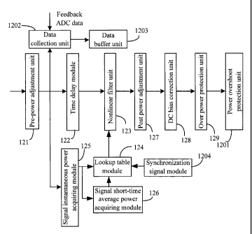
[0041] Figure 1 is a structural diagram of a device according to an embodiment
of the present
invention;
[0042] Figure 2 is a structural diagram of a pre-distorter in the device shown
in Figure 1;
[0043] Figure 3 is a structural diagram of a nonlinear filter unit in the pre-
distorter shown in Figure
2;
[0044] Figure 4 is a schematic diagram of a lookup table switching policy in
the pre-distorter
shown in Figure 2;
[0045] Figure 5 illustrates a timing relationship between a power abnormity
signal and a
synchronization signal of a base station transmitter according to an
embodiment of the present
invention;
[0046] Figure 6 shows a flow chart of calculating a nonlinear filter parameter
in an adaptive
parameter calculation unit in the device shown in Figure 2;
[0047] Figure 7 shows a selection procedure in a method for selecting a peak
sample according to
an embodiment of the present invention;
[0048] Figure 8 is a structural diagram of a simplified pre-distorter
according to an embodiment of
the present invention;
[0049] Figure 9 is a structural diagram of a QMC network in the pre-distorter
shown in Figure 8;
[0050] Figure 10 is a structural diagram of a nonlinear filter unit in the pre-
distorter shown in
Figure 8;
[0051] Figure 11 is a structural diagram of an improved pre-distorter
according to an embodiment
of the present invention; and
[0052] Figure 12 is a structural diagram of a digital modulator in the pre-
distorter shown in Figure
11.
8
CA 02609843 2007-11-26
Detailed Descriptions of the Embodiments
[0053] The present invention provides a device for pre-distorting a base-band
digital signal. The
essence of the present invention lies in that filter coefficients in a pre-
distorter may follow the
change of the characteristics of a power amplifier. This may be implemented by
use of a lookup
table. Accordingly, good radio frequency characteristics of an output signal
may be achieved.
[0054] The device according to the present invention will be detailed with
reference to the
drawings. Figure 1 shows a device for pre-distorting a base-band digital
signal according to the
present invention which processes the base-band digital signal as follows:
[0055] Multi-carrier I, Q signals transmitted from a base-band modem 110 are
pre-distorted by a
pre-distorter 120, and the distorted multi-carrier I, Q signals are sent
respectively to a first
Digital-to-Analog Converter (DAC) 131 and a second Digital-to-Analog Converter
(DAC) 132.
The first and second DACs 131 and 132 convert the I, Q signals into analog
zero
intermediate-frequency I, Q signals respectively, and then an IQ modulator 140
performs an
Analog Quadrature Modulation (AQM) to the analog zero intermediate-frequency
I, Q signals, so
that the signals are up converted into radio frequency. Then the signals are
amplified, attenuated
and impedance matched through a radio frequency channel, and then sent to a
power amplifier
150 for power amplification.
[0056] A part of the signal output from the power amplifier 150 is transmitted
by an antenna 200
via a duplexer, and the remaining part of the signal is fed back by a coupler
160 to a detection
channel, converted by a down converter 170 into analog intermediate frequency,
and sampled by a
high speed Analog-to-Digital Converter (ADC) 180. The high speed Analog-to-
Digital Converter
(ADC) 180 outputs a digital intermediate feedback signal, which is then sent
to the pre-distorter
120.
[0057] The digital intermediate-frequency feedback signal and the multi-
carrier I, Q signals which
are input into the pre-distortion system are sampled and buffered in the pre-
distorter 120, and the
buffered signals are sent to an adaptive parameter calculation unit 190 via an
interface between
the pre-distorter 120 and the adaptive parameter calculation unit 190.
[0058] The adaptive parameter calculation unit 190 calculates the filter
parameters based upon the
received signals by using an adaptive correction algorithm, and sends the
calculated filter
parameters to the pre-distorter 120. The calculated filter parameters are then
stored in a lookup
table module 124 (shown in Figure 2) of the pre-distorter 120. The pre-
distorter 120 selects the
appropriate filter parameters depending upon the practical requirements to pre-
distort the signals.
[0059] In an embodiment of the present invention, the pre-distorter 120 is
typically implemented
with a Field Programmable Gate Array (FPGA) or an Application Specific
Integrated Circuit
(ASIC) for the purpose of real-time correction of the base-band I, Q signals.
Because the
9
CA 02609843 2007-11-26
characteristics of the power amplifier changes slowly, and the updating of
filter parameters may
be enabled offline in a non-real-time manner, the adaptive parameter
calculation unit 190 is
typically implemented by using a Digital Signal Processor (DSP).
[0060] The core part of the device according to the embodiment of the present
invention is the
pre-distorter 120. The main characteristic of the pre-distorter 120 lies in
that, its nonlinearity
characteristic is reciprocal to that of the radio frequency channel including
the power amplifier.
[0061] If the real part, the imaginary part and the instantaneous amplitude of
a complex signal
input into the pre-distorter 120 are denoted by Ii,(-), Q1, (=) and Mg,,(-)
respectively, the real and
imaginary parts of a complex signal output from the pre-distorter 120 Ioõt(=)
and Q0õ((=) may be
expressed by
M-1
IouT(k) = io + J[a(m)f (Mg;,, (k -m))I,,, (k -m) +b(m)f (Mgrõ (k -m))Q.,, (k -
m)]
M=O
M-1
QouT(k) = qa + J[c(m) f (Mgrõ (k -m))Irõ (k -m) +d(m) f (Mg;,,(k -m))Q.,, (k -
m)]
nr~o
[0062] Here, f(=) denotes a nonlinear function for correcting the nonlinearity
of the radio
frequency channel, i.e. an inverse function of the nonlinearity characteristic
of the radio
frequency channel. This function may be selected based upon the
characteristics of the power
amplifier 150, the system-required characteristics of a radio frequency output
signal and the
calculation capability supported by the system. The M in the above equations
denotes a time
constant of a power amplifier memory effect which may be corrected by the pre-
distorter 120.
The larger the M, the more precise but the more complex the calculation in the
pre-distorter
would be. The corresponding parameters have to be selected reasonably to
represent the
compromise between the system requirements and the cost. The inverse nonlinear
function f(=) of
the radio frequency channel may be expanded by using various base functions,
for example, a
power function, a Legendre function, etc.
[0063] In the case of a power function, this nonlinear function may be
expressed by
N-1
f (X) = an,xna
n=0
[0064] Here, an denotes an expansion coefficient, and a denotes the lowest
order of the power
function, and may be selected as an integer or fraction. The smaller the c the
larger an order N
of the base function is, the more precise the pre-distortion model is, the
higher the algorithm
performance is, but the more complex the calculation would be. Thus, the
corresponding
parameters have to be selected reasonably to represent the compromise between
the system
CA 02609843 2010-08-16
requirements and cost.
[0065] In the case of a Legendre function, this nonlinear function may be
expressed by
N-1
f(x)aõPõ(x)
n=O
[0066] Here, P,,,(x) denotes an n-order Legendre function, a, denotes an
expansion coefficient, and
N is the number of items in the expanded polynomial. Similarly, the larger the
N, the more
precise the pre-distortion model is, the higher the algorithm performance is,
but the more
complex the calculation would be.
[0067] As can be seen from the above, each of the I, Q signals output from the
pre-distorter 120 in
the embodiment of the present invention may be regarded as a sum of outputs of
two Finite
Impulse Response (FIR) filters which respectively filter the input I, Q
signals. Different from the
conventional FIR filter, however, coefficients of these filters depend upon
the amplitude of an
input signal, and this dependency may be expressed by function fl-). The
function fl*) (=) may be
searched for in a lookup table in accordance with the amplitude of an input
signal, for example,
for Mgin(n), a corresponding f (Mg,n(n)) may be found.
[0068] As shown in Figure 2, the pre-distorter 120 according to an embodiment
of the present
invention includes the following modules:
[0069] 1. a pre power adjustment unit 121: this unit is adapted to adjust the
power of a signal
output from a base-band modem 110, and send the adjusted signal to a time
delay module 122.
The pre-power adjustment unit 121 is designed to prevent the input signal from
being saturated
after passing the pre-distorter 120, and may be implemented with a simple
scalar multiplier .
[0070] 2. a time delay module 122: this module is adapted to delay the data
stream of a signal, so
as to ensure the coefficients of an FIR lookup table used for FIR calculation
to match the samples
used by a signal instantaneous power acquiring module 125 and a signal short-
time average power
acquiring module 126 for calculating the index of the lookup table, and send
the delayed signal to
a nonlinear filter unit 123.
[0071] 3. a nonlinear filter unit 123: this unit is a core part in the pre-
distorter 120. As shown in
Figure 3, the nonlinear filter unit 123 is implemented as an M-tap FIR filter
with variable
coefficients, includes delay modules 1231, :multiplier modules 1232 and an
accumulator module
1233.
100721 Each of the delay modules 1231 is adapted to delay the data streams of
I, Q 'components of
an input signal, and send the delayed input signal to a corresponding :
multiplier module 1232.
[0073] Each of the multiplier modules 1232 is adapted to complex multiplying
the input signals
11
CA 02609843 2010-08-16
respectively in accordance with the received and delayed I, Q components of
the input signals as
well as the corresponding four nonlinear filter parameters, and output the
multiplied signals to the
accumulator module 1233.
[0074] Each of the multiplier modules 1232 is provided with two I and Q signal
inputs, four filter
parameter inputs, and two I and Q signal outputs, and may correct the
different delays of the I, Q
analog signals resulted from. transmission effectively. Assume that the I, Q
signals input into one
of the multiplier modules 1232 are denoted by I and Q6 and the four input
filter parameters are
denoted by Tu, Tiq Tqi and Tqq, then the output I, Q signals Oi and Qq may be
denoted by
O,=I,xTõ+Q;xT;q
Oq = I, x T9, + Q, x T~
[0075] The four filter parameters Tii, Tiq, Tqi and Tqq correspond to the four
parameters a, b, c and d
contained in the equation showing the relationship of an output complex signal
and an input
complex signal of the pre-distorter 120, respectively. The parameters T may be
determined
according to the instantaneous power and the short-time average power of the
signals and a
synchronization signal, and may be found through searching in a lookup table
module 124 in the
pre-distorter 120.
[0076] The accumulator module 1233 is adapted to accumulate the received
signals output from
the multiplier modules 1232, and output the accumulated signals to a post
power adjustment unit
127.
[0077] 4. a lookup table module 124: this module is adapted to store and
update the nonlinear filter
, parameters calculated by the adaptive parameter calculation unit 190, select
nonlinear filter
parameters according to the received statistic results of instantaneous power
and short-time
average power of an input signal as well as the order number of taps of the
nonlinear filter unit
123, and send the selected nonlinear filter parameters to the nonlinear filter
unit 123.
[0078] Various nonlinear filter parameters and various nonlinear inverse
functions A-) are stored
in the lookup table module 124. The lookup table is of three dimensions
determined by
instantaneous power, short-time average power of a signal and an order number
of taps
respectively. A nonlinear inverse function f-) defines a nonlinear
relationship between the
instantaneous power of an signal, and an output signal. The short-time average
power defines an
operation point and a temperature of the power amplifier 150, while different
short-time average
powers correspond to different characteristics of the power amplifier 150.
Consequently, different
nonlinear inverse functions shall be selected for different short-time average
powers. The taps
define the correction characteristics of a memory effect of the radio
frequency channel. Different
nonlinear inverse functions shall be selected according to different taps.
[0079] The nonlinear filter parameters stored in the lookup table need to be
updated in accordance
12
CA 02609843 2007-11-26
with the calculation result of the adaptive parameter calculation unit 190.
When updating the
nonlinear filter parameters stored in the lookup table, only one set of
parameters therein may be
updated at one time. This set of nonlinear parameters may be in use during the
updating, while the
power of the signal output from the transmitter shall remain substantially
stable during a period of
time. Therefore, in order to ensure a good quality of the signal output from
the transmitter during
the updating of the lookup table, a redundant dynamic switching method may be
used for the
updating of the parameters in the lookup table according to an embodiment of
the present
invention. The basic principle of this method will be described below.
[0080] If N sets of nonlinear filter parameters are needed to ensure a stable
quality of the signal
output from the system, N+1 sets of nonlinear filter parameters may be
provided in the
pre-distorter 120, respectively indexed with 0, 1, 2. ......, N, where the
0th, 1st 2nd, , (N-1)th
sets of nonlinear filter parameters are used for the practical application,
and the Nth set is used as a
switching buffer, which is allocated dynamically in use. If the set of
nonlinear filter parameters
indexed with M need to be switched in an example, the memory states of the
lookup table before
and after the switching are as shown in Figure 4.
[0081] Before the switching, the pre-distorter 120 utilizes the sets of
nonlinear filter parameters
indexed with 0, 1, 2. ......, N-1, while the set of nonlinear filter
parameters indexed with N is
used for switching. If the set of nonlinear filter parameters indexed with M
need to be switched in
the example, the adaptive parameter calculation unit 190 firstly writes a new
set of filter
parameters into the set of nonlinear filter parameters currently indexed with
N via an interface
provided by the pre-distorter 120. At this time, the original set of nonlinear
filter parameters
indexed with M are in use, thus the adaptive parameter calculation unit 190
notifies, via an
interface, the pre-distorter 120 that the index number of the set of nonlinear
filter parameters
which need to be switched is M. Then the pre-distorter 120 changes the index
number of the set of
nonlinear filter parameters, which were originally indexed with M, into N, and
changes the index
number of the set of nonlinear filter parameters, which were originally
indexed with N, into M.
The new set of nonlinear filter parameters indexed with M will be used in the
subsequent
real-time data processing.
[0082] This redundant dynamic switching method may effectively prevent the
nonlinear filter
parameters being in use from being changed dynamically, thereby ensuring a
stable quality of the
output signal.
[0083] Furthermore, in practical implementation, it generally takes a certain
period of time to
carry out a statistic of the short-time average power of a signal. During this
period of time, only
one set of nonlinear parameters may be in use. At this time, the addressing
for other sets of
parameters may be disabled, thus the powering current for these inactive
signals may be reduced,
so as to achieve a lower power consumption.
13
CA 02609843 2010-08-16
[0084] 5. a signal instantaneous power acquiring module 125: this module is
adapted to acquire
the instantaneous power of a signal by first calculating the squared sum of I,
Q components and
then calculating square root of the squared sum, and send the calculation
result to the lookup table
module 124 so as to select filter parameters.
[0085] 6. a short-time average power acquiring module 126: this module is
adapted to acquire the
short-time average power of a signal by calculating the average value of the
instantaneous powers
of adjacent N points of the signal, and send the calculation result to the
lookup table module 124
so as to select filter parameters.
[0086] 7. a post power adjustment unit 127: this unit is adapted to adjust the
power of a signal
output from the pre-distorter 120, and send the adjusted signal to a direct-
current bias correction
unit 128. The post power adjustment unit 127 is provided to ensure that the
power of a signal
output from the power amplifier satisfies the design requirement. The post
power adjustment unit
127 may be implemented by a simple multiplier ; The post power adjustment unit
127 may
achieve the function of stabilizing the power of the transmitter, by
cooperating with a numerically.
controlled radio frequency attenuator.
[0087] 8. a direct-current bias correction unit 128: this unit is adapted to
adjust the direct-current
bias of an output digital signal, and send the adjusted signal to an over
power protection unit 129.
[0088] 9. an over power protection unit 129: this unit is adapted to detect
the average power of an
output digital signal, and limit the amplitude of the output signal if the
average power is greater
than a threshold so as to prevent the calculation error of the method and thus
protect the power
amplifier. The output signal of the over power protection unit 129 is sent to
a power overshoot
protection unit 1201.
[0089] 10. a power overshoot protection unit 1201: this unit is adapted to
detect the instantaneous
power of an output digital signal, and determine the occurrence of power
overshoot if a proportion
of the instantaneous power greater than the threshold is greater than a
predefined proportion. In .
the case of power overshoot, the system may directly cause the pre-distorter
120 to stop outputting
signal, so as to prevent the power amplifier from being burnt down. After the
power overshoot
disappear, the output of the pre-distorter 120 will be recovered quickly, so
as to ensure the normal
communication on the link. The pre-distorter 120 outputs the signal via the
power overshoot
protection unit 1201.
[0090] 11. a data capture unit 1202: this unit is adapted to sample a certain
length of continuous
base-band I, Q signals as well as a feedback ADC signal, and send the sampled
signals to a data
buffer unit 1203.
[0091] 12. a data buffer unit 1203: this unit is adapted to store the base-
band I, Q signals and the
feedback ADC signal sampled by the data capture unit 1202. The signals stored
in the buffer unit
14
CA 02609843 2007-11-26
1203 are sent to the adaptive parameter calculation unit 190 via an interface
between the
pre-distorter 120 and the adaptive parameter calculation unit 190, so that the
adaptive parameter
calculation unit 190 may calculate and update the filter parameters in the
lookup table.
[0092] 13. a synchronization signal module 1204: this module is adapted to
control the selection of
the filter parameters in the lookup table, and control the selection of the
sampled signals by the
data capture unit in the case of a base-band signal abnormity.
[0093] A synchronization signal may be sent in a base-band data stream to the
pre-distorter 120
through a hardware connection, or may be directly acquired from the base-band
I, Q data stream
through a simple detection mechanism inside the pre-distorter 120 if it is
easy to detect a signal
abnormity.
[0094] In the 3G system or the like, in order to locate a user, a base station
transmitter may
sometimes switch off or reduce the signal output for a while to reserve
certain timeslots for the
user for location calculation. Alternatively, during data communication, the
base station
transmitter may periodically transmits a large pilot signal when there is no
access of a user, and
reduce the transmission power or switch off the signal when there is still no
access of a user. Each
of these abrupt changes of the signal power may be considered as a power
abnormity. In these
cases, the synchronization signal of the power signal is needed for special
processing.
[0095] The timing relationship between a power abnormity signal and a
synchronization signal is
as shown in Figure 5.
[0096] Because the base station transmitter presents an apparent nonlinearity
in the case of a large
signal, the base station transmitter takes the high-power portion of the
signal as a normal signal
power and takes the low-power portion as an abnormal signal power. It is
necessary for the active
portion (i.e., the low-level portion) of the synchronization signal to include
all the moments at
which the signal power is reduced abnormally, so as to achieve effective
signal synchronization.
In other words, t1 and t2 as shown in Figure 5 are both larger than zero
(where tl is the time
difference between the falling edge of the synchronization signal and
occurrence of a signal
power abnormity, and t2 is the time difference between the recovery moment
from the signal
power abnormity and a rising edge of the synchronization signal). The
synchronization signal
enters a low-level (active) state prior to the occurrence of the power
abnormity, and enters a
high-level (inactive) state after the recovery from the power abnormity.
Unfortunately, this timing
may be difficult to implement in the system, because it is impossible to
predict an abnormity of
the signal power. For the purpose of implementing the timing, the falling edge
of the
synchronization signal may be allowed to lag slightly behind the falling edge
of the signal power,
but it should be ensured that the synchronization signal appears in a low
level before the detection
mechanism of short-time average power in the pre-distorter 120 calculates that
a short-time power
decision switching occurs. Also, for the purpose of preventing any influence
on the pre-distorter
CA 02609843 2007-11-26
120 in the processing of a normal signal, the durations of tl and t2 should be
selected reasonably
depending on the system requirement, and should not be over long. Preferably,
the durations of tl
and t2 may be -3 s < tl < 10 s, and 0 < t2 < 10 s.
[0097] The synchronization signal may have an influence on the function of
short-time average
power calculation and decision and the function of signal sampling in the pre-
distorter 120.
Therefore, if the synchronization signal is in a low-level (i.e., active), the
calculation of the
short-time average power should be stopped, while the originally calculated
value is kept
unchanged. The calculation of the short-time average power should not be
recovered until the
synchronization signal enters a high level. Also, in the case of the
synchronization signal in an
active low-level, the data capture unit of the pre-distorter 120 should stop
the sampling of the
base-band and feedback data, and the sampling should not be recovered until
the synchronization
signal enters a high level.
[0098] The adaptive parameter calculation unit 190 in the device according to
the embodiment of
is adapted to calculate nonlinear filter parameters, with a structure as shown
in Figure 6. The
adaptive parameter calculation unit 190 includes the following modules.
[0099] A Demodulation module 191: this module is adapted to demodulate a
feedback digital
intermediate-frequency signal.
[00100] The demodulation is to recover the feedback I, Q signals from the
feedback digital
intermediate-frequency signal. In particular, the demodulation may be
implemented by the
following method: First, two orthogonal components (i.e. a sine component and
a cosine
component) of the carrier of the intermediate-frequency signal are recovered
in the adaptive
parameter calculation unit 190 because the feedback intermediate-frequency
points are known
during the design of the system. Then the sampled intermediate-frequency
signal is multiplied
with the cosine component of the carrier, and the multiplied signal is low-
pass filtered, thus the
feedback I signal is obtained. The feedback Q signal may be obtained by
multiplying the sampled
intermediate-frequency signal with the sine component of the carrier and low-
pass filtering the
multiplied signal.
[00101] A delay and matching module 192: this module is adapted to delay and
match the
base-band I, Q signals with the feedback I, Q signals.
[00102] The delay and matching is to align the base-band I, Q signals with the
feedback I, Q signals
in time by using a correlation algorithm. In the correlation algorithm, the
cross-correlation
function between the base-band I, Q signals and the feedback I, Q signals is
calculated, the
location where a peak occurs is acquired, the index number of the location
corresponds to the
delay value of the feedback signals relative to the base signals. Then the
redundant portions of the
base-band and feedback signals are removed according to the calculated delay
value, so as to
16
CA 02609843 2007-11-26
obtain the delayed and matched base band I, Q signals and feedback I, Q
signals.
[00103] A frequency shift/phase shift correction module 193: this module is
adapted to correct the
frequency shift and the phase shift between the base-band signals and the
feedback signals.
[00104] A frequency shift and a phase shift may exist between the base-band
signals and the
feedback signals. The frequency shift and a phase shift between the base-band
signals and the
feedback signals should be corrected, so as to calculate a pre-distortion
function properly. This
correction may be done by the following method: first, the phase difference
between the
base-band signals and the feedback signals is calculated; the accurate values
of the frequency shift
and the phase shift may be obtained by using the least square algorithm,
because the frequency
shift and phase shift correspond to the slope and the intercept of the phase
difference-time linear
function respectively. Then, feedback I, Q signals with neither frequency
shift nor phase shift may
be obtained by removing the accurate values of the frequency shift and the
phase shift directly
from the feedback signals.
[00105] An optimal signal selection module 194: this module is adapted to
select optimal data from
the base-band signals and the feedback signals.
[00106] The procedure of calculating the nonlinear filter parameters in the
adaptive parameter
calculation unit 190 is very complex, thus the calculation amount will be
considerable if all the
base-band and feedback I, Q signals are used in the calculation of parameters,
which exceeds the
processing capability of the digital signal processing chips available in the
industry. Therefore,
representative data for calculation of nonlinear filter parameters should be
selected from the
base-band and feedback I, Q signals acquired from sampling, so as to obtain an
achievable
calculation amount.
[00107] With an analysis of the digital signal characteristics of the
transmitter and the nonlinearity
characteristics of the transmission channel, the embodiments of the present
invention present two
method for selecting optimal data from the base-band and feedback signals, one
is a peak sample
selection method, and the other is a random sample selection method.
[00108] In the peak sample selection method, it is considered that the power
amplifier is the most
sensitive to the instantaneous power of a signal in the nonlinear system of
the transmission
channel. During the selection of an optimal signal, the selection shall be
made from signal
samples with the following features:
[00109] 1. Peak amplitude: i.e., a sample having peak signal instantaneous
amplitude.
[00110] 2. Peak IQ value: i.e., a sample having peak absolute value of I or Q
signal.
[00111] 3. Peak variation: i.e., a sample, the two adjacent signal samples of
this sample have a peak
variation in amplitude or I, Q values.
17
CA 02609843 2010-08-16
[00112] A particular implementation of the peak sample selection method is as
follows: Assume
that S is the number of optimal samples for calculation acceptable by the
system, then N peak
samples are selected from the samples with the above peak values. Each of the
selected peak
samples is then taken as a center, and S/2N samples are selected respectively
on the left and right
of each center. As a result, the total number of the selected samples is:
N
N - )xN=S
(2+ S
[00113] A desired number of samples may be obtained. If several samples on the
left or right of the
peaks of the I or Q signal overlap, the overlapping samples shall be used for
calculation only once,
and the numbers of sample(s) around the overlapping samples are increased
respectively so as to
ensure a constant total number. Additionally, some random samples may be
inserted when
appropriate in the peak sample selection method, so that the data may be
sufficiently
representative of the signals.
[00114] A selection procedure in the peak sample selection method according to
an embodiment of
the present invention is as shown in Figure 7. Assume that S is the number of
optimal samples for
calculation, then the signals may be divided into 6 segments in the method.
Maximum values and
minimum values of I, Q signals are selected in the signal data stream, and
there are totally 4
segments, each with a length of S/6. Further S/6 samples are selected at the
beginning and end
respectively as random filling data. As can be seen from Figure 7, there is
overlapping between
the data segments corresponding to the maximum values of I and the minimum
values of Q. In
this regard, additional samples are selected on the left of the samples
selected based upon the
maximum values of I, and on the right of the samples selected based upon the
maximum values of
Q, so that the total number of samples, i.e. S, remains constant.
[00115] . The principle of the random sample selection method lies in that:
samples with different
signal amplitudes shall be selected, and preferably, the selected samples may
have a distribution
characteristic identical with that of amplitudes prior to the selection, so as
to model the nonlinear
system effectively.
[00116] Consequently, a particular implementation of the random sample
selection method is as
follows: A random seed is selected, and multiplies of this random seed are
used in selection of signal
samples in the signal. The amplitude range corresponding to the signal is
recorded. If recorded data within
this range is not sufficient to satisfy a predetermined requirement, the data
is recorded, otherwise the data
is dropped. This above procedure is repeated until sufficient samples are
selected.
[00117] A nonlinear parameter resolution module 195: this module is adapted to
calculate
nonlinear filter parameters in accordance with the selected optimal data.
[00118] Currently, there are many matured algorithm such as Recursive Least
Square (RLS), Least
18
CA 02609843 2010-08-16
Mean Squares (LMS), QR Recursive Least Square (QR-RLS), etc., which may be
used to
calculate nonlinear filter parameters in accordance with the selected optimal
data according.to an
embodiment of the present invention.
[00119] Based upon the structure of the above described adaptive parameter
calculation unit, a
method for calculating nonlinear filter parameters is provided according to an
embodiment of the
present invention. This method includes the procedures of:
[00120] 1. demodulating a feedback digital signal;
[00121] 2: delaying and matching the demodulated feedback signal and a base-
band signal;
[00122] 3. calculating the frequency shift and the phase shift between the
base-band signal and
feedback signal by using the least square algorithm, and correcting the
frequency shift and the
phase shift of the delayed and matched feedback signal and base-band signal;
[00123] 4. selecting optimal data from the feedback signal and base-band
signal after the frequency
shift and phase shift correction by using the peak sample selection method and
the random sample
selection method;
[00124] 5. calculating nonlinear filter parameters in accordance with the
selected optimal data by
using a certain algorithm.
[00125] An embodiment of the present invention provides a simplified pre-
distorter. The structure
of the simplified pre-distorter is as shown in Figure 8. In comparison with
Figure 2, a Quadrature
Modulation Compensation (QMC) network is used instead of the direct-current
bias correction
unit, and the internal structure of the nonlinear filter unit 125 is also
simplified.
[00126] The QMC network 810 is adapted to correct the IQ gain, the phase
imbalance and the
direct-current bias. As illustrated by the structure shown in Figure 9, the
QMC network 810
includes four multipliers 811 and four adders 812 which perform the
calculation operations as
shown in Figure 9. The values of two direct-current bias correction parameters
bcl and bc2 in
the QMC network are equivalent to the two direct-current correction parameters
of the
direct-current corrector as shown in Figure 2. Gain-imbalance correction
parameters acl and ac2
and a phase-imbalance correction parameter (pc may be calculated in accordance
with the four
parameters a, b, c and d in the above described implementation of the pre-
distorter.
[00127] In this manner, the number of parameters input into an FIR filter may
be reduced from four
to two, thus half of the system memories may be saved.
[00128] In the nonlinear filter unit 125 of the simplified pre-distorter, each
of the taps of the filter is
provided with two I, Q signal inputs, two filter parameter inputs, and two I,
Q signal outputs. The
structure of. the M-tap nonlinear filter unit 125 is as shown in Figure 10,
where the I, Q input
19
CA 02609843 2010-08-16
signals and the coefficients of each tap are multiplied as the following
equations:
O,=I,xT,-Q,xTq
Oq=I;xTq+Q,xT;
[00129] Here, 0 denotes an output signal, Oi and Oq respectively denote I, Q
components of an
output signal, Ii. and Qq respectively denote I, Q components of an input
signal, and T denotes a
filter coefficient. The parameter T may be selected depending upon the
instantaneous power and
the short-time average power of a signal as well as a synchronization signal,
as in the method for
parameter selection in the non-simplified pre-distortion FIR filter.
[00130] In the device according to an embodiment of the present invention,
there may be. a risk in
the use of the IQ demodulator of the device as shown in Figure 1 to convert a
signal from radio
frequency into intermediate frequency if the transmitter imposes a strict
requirement on local
oscillation leakage and the IQ gain and phase imbalance of a signal. In view
of this, an
embodiment of the present invention provides an improved pre-distorter, which
is as shown in
Figure 11.
[00131]. In the improved pre-distorter, a conventional double frequency
conversion technology is
adopted. In the double frequency conversion, first the IQ signals are
modulated to a digital
intermediate frequency in the pre-distorter, then the signals output from the
pre-distorter are
digital-to-analog converted into digital intermediate-frequency signals, and
finally the digital
intermediate-frequency signals are converted to radio frequency. In the
structure of the improved
pre-distorter, a digital modulator 910 is used instead of the QMC network in
Figure 8 and the
direct-current bias correction unit in Figure 2.
[00132] As illustrated by the structure as shown in Figure 12, the digital
modulator includes five
parts, i.e., a Numerically Controller Oscillator (NCO) 911, two multiplexers
912, a 90 phase,
shifter 913 and an adder 914. A particular operation flow of the digital
modulator is shown as
follows:
25f001331 In step 12-1, the NCO 911 generates a desired digital intermediate-
frequency local
oscillation sine signal.
1001341 In step 12-2, the 90 phase shifter 913 shifts the phase of the local
oscillation sine signal
obtained in step 12-1 by 90 , so as to obtain a local oscillation cosine
signal.
{00135] In step 12-3, the local oscillation sine signal is multiplied with the
input I signal, and the
local. oscillation cosine signal is multiplied with the input Q signal,
respectively in the two
multipliers 912.
[00136] In step 12-4, the two multiplied signals obtained in step 12-3 are
added up in the adder 914
so as to obtain an output signal of the digital modulator 910.
CA 02609843 2007-11-26
[00137] Accordingly, a method for pre-distorting a base-band digital signal
according to an
embodiment of the present invention includes the procedures of:
[00138] calculating nonlinear filter parameters in accordance with samples of
a received base-band
digital signal and samples of a feedback signal of a radio frequency channel;
[00139] performing power statistics of the input base-band digital signal,
selecting nonlinear filter
parameters corresponding to the result of the power statistics, pre-distorting
the base-band digital
signal, and outputting the pre-distorted base-band digital signal.
[00140] In particular, the pre-distorting includes the process of delaying the
data stream of the input
signal, performing calculation operation for the delayed multi-stage input
signals and the
corresponding nonlinear filter parameters, and generating and outputting the
output signal.
[00141] In an embodiment of the present invention, the pre-distorting includes
the procedures of:
[00142] delaying data streams of the I, Q components of the input signal;
[00143] complex multiplying the input signal in accordance with the received
and delayed I, Q
components of the input signal and the corresponding nonlinear filter
parameters, accumulating
the multiplied signal, and outputting the multiplied signal.
[00144] In the complex multiplying, a relationship between the input signal
and the output signal
may be expressed by
0,= I,xT,.,+Q,xT"
Oq =I, xT1+Q, xTgq
[00145] Here, I, and Q, respectively denote the I, Q components of the input
signal, T,,, T,q, Tq, and
Tqq respectively denote the received four filter parameters, and O, and Qq
respectively denote the I,
Q components of the output signal.
[00146] Optionally, in the complex multiplying, a relationship between the
input signal and the
output signal may be expressed by
0,= I,xT,-Q,xTq
Oy =I,xTq+Q,xT,
[00147] Here, I, and Qq respectively denote the I, Q components of the input
signal, T, and Tq
respectively denote the received corresponding two filter parameters, and O,
and Oq respectively
denote the I, Q components of the output signal.
[00148] The power statistics includes calculating the instantaneous power of
the input signal and
calculating the short-time average power of the input signal.
21
CA 02609843 2007-11-26
[00149] The procedure for selecting nonlinear filter parameters includes
selecting the nonlinear
filter parameters in accordance with the calculation results received from a
signal instantaneous
power acquiring module and a signal short-time average power acquiring module,
as well as the
order number of the taps of the nonlinear filter unit.
[00150] As discussed previously, the nonlinear filter parameters may be
updated redundantly and
dynamically according to an embodiment of the present invention.
[00151] Furthermore, in the case of an abnormity in the base-band signal, a
synchronization signal
of the base-band signal may be provided to the pre-distorter, and may be used
to control the
selection of the nonlinear filter parameters, to control the pre-distorter so
that the sampling of the
base-band and feedback data may be stopped temporarily in the case of the
abnormity in the
base-band signal.
[00152] The procedure for calculating nonlinear filter parameters includes:
[00153] demodulating the feedback digital intermediate-frequency signal into
feedback IQ signals;
delaying and matching received base-band IQ signals and the feedback IQ
signals; correcting the
frequency shift and phase shift between the delayed and matched base-band IQ
signals and the
feedback IQ signals; selecting optimal data from the corrected base-band IQ
signals and the
feedback IQ signals; and calculating the nonlinear filter parameters in
accordance with the
selected optimal data.
[00154] While the preferred embodiments of the present invention have been
described as above,
the scope of the present invention shall not be limited to these embodiments.
Indeed,
modifications or alternatives which may occur to those skilled in the art in
light of the disclosure
of the present invention shall fall within the scope of the present invention
as defined in the
accompanying claims.
22