Note: Descriptions are shown in the official language in which they were submitted.
CA 02611916 2007-12-11
1
DESCRIPTION
IMAGING APPARATUS AND METHOD OF MANUFACTURING THE SAME
TECHNICAL FIELD
[0001] The present invention relates to an imaging
apparatus which acquires an image of an object by receiving
light from the object and performing a photoelectric
conversion, and a method of manufacturing the imaging
apparatus.
BACKGROUND ART
[0002] Conventionally, a small imaging apparatus is
proposed for incorporation into digital cameras, video
cameras, and portable terminals such as mobile telephones
and Personal Digital Assistants (PDA) provided with a
function of camera. The imaging apparatus acquires an
image of an object by receiving light from the object and
performing photoelectric conversion of the received light.
Such an imaging apparatus includes a solid-state imaging
sensor such as a charge coupled device (CCD) or a
complementary metal-oxide semiconductor (CMOS) image sensor,
and an optical system which focuses light from the object
on a light receiving surface of the solid-state imaging
sensor to form the image (see, Patent Document 1, for
example).
[0003] In recent years, such an imaging apparatus has
come to be incorporated into medial devices such as
endoscopes and capsule endoscopes. These medical devices
are employed for observation of an inside of alimentary
tracts of a subject, for example. Therefore, further
downsizing of the imaging apparatus is highly desirable.
For the downsizing, the imaging apparatus is formed of a
CA 02611916 2007-12-11
2
chip-size package (CSP) type solid-state imaging sensor.
The CSP is a package of substantially the same outer
dimension as a semiconductor chip. FIG. 8 is a schematic
cross-sectional view showing a side cross section structure
of a conventional imaging apparatus including such a CSP-
type solid-state imaging sensor
[0004] As shown in FIG. 8, a conventional imaging
apparatus 101 includes a CSP-type solid-state imaging
sensor 102 which has a light receiving unit 102a for
reception of light from an object, an optical system 103
which focuses light from the object on a light receiving
surface of the light receiving unit 102a, a circuit board
104 on which the solid-state imaging sensor 102 is mounted,
and a resin material 105 which reinforces the packaging
strength of the solid-state imaging sensor 102 and the
circuit board 104. The solid-state imaging sensor 102 has
a cover glass 102b which protects a semiconductor chip (CCD
chip, for example) on which the light receiving unit 102a
is formed, and solder balls 102c. The optical system 103
includes a lens 103a which focuses light from the object
onto the light receiving unit 102a, a barrel member 103b
which protects the lens 103a and delineates a light
receiving region 103d on a surface of the cover glass 102b,
and a light blocking wall 103c which shields a region
outside the light receiving region 103d of the cover glass
102b from light. The barrel member 103b has a through hole
inside. An opening at one end of the through hole is
closed by holding the lens 103a, whereas an opening at
another end of the through hole delineates the light
receiving region 103d on the cover glass 102b at a position
corresponding to the light receiving unit 102a. The light
blocking wall 103c has a substantially reverse-U-shaped
cross section. The light blocking wall 103c engages with
CA 02611916 2007-12-11
3
the cover glass 102b so as to cover a region (upper surface
and side surfaces of the cover glass 102b) other than the
light receiving region 103d of the cover glass 102b.
[0005] When the imaging apparatus 101 is employed for
imaging of the object, light from the object comes into the
barrel member 103b through the lens 103a, and passes
through the light receiving region 103d to be focused onto
the light receiving surface of the light receiving unit
102a. The light receiving unit 102a then, performs
photoelectric conversion on the focused light from the
object, to generate an image signal of the object. Here,
since the light blocking wall 103c blocks the light so that
the light would not be incident on the region other than
the light receiving region 103d of the cover glass 102b,
the light receiving unit 102a receives only the light that
comes from the object and enters into the barrel member
103b through the lens 103a.
[0006] Patent Document 1: JP-A No. 2003-110945 (KOKAI)
DISCLOSURE OF INVENTION
PROBLEM TO BE SOLVED BY THE INVENTION
[0007] In the above-described conventional imaging
apparatus 101, a light-blocking element is provided to
shield the region outside the light receiving region 103d
of the cover glass 102b so that unnecessary external light
other than the light from the object is prevented from
coming in. For the light shielding, a depressed portion of
the light blocking wall 103c that engages with the cove
glass 102b is required to have a close possible dimension
(height, width, depth) to an outer dimension (height, width,
depth) of the cover glass 102b, so that there is little gap
between the engaging depressed portion of the light
blocking wall 103c and the cover glass 102b when the light
CA 02611916 2007-12-11
28964-146
4
blocking wall 103c is attached to the cover glass 102b.
Hence, highly accurate positioning of the engaging portion
of the light blocking wall 103c and the cover glass 102b is
required at the attachment of the light blocking wall 103 to
the cover glass 102b. In many cases, an optical system
including such a light blocking wall is difficult to be
attached to the solid-state imaging sensor, which makes
manufacturing of the imaging apparatus difficult.
[0008] In addition, it requires enormous time and efforts
to prepare an optical system with such a light blocking wall
for each solid-state imaging sensor in accordance with a
chip size of a semiconductor chip on which the solid-state
imaging sensor is mounted, i.e., in accordance with the
outer dimension of the cover glass. Still in addition, the
above-described light blocking wall contributes to an
undesirable upsizing of the imaging apparatus. The
endoscope or capsule endoscope incorporating the imaging
apparatus tends to have a larger casing corresponding to the
size of the imaging apparatus, whereby downsizing of the
endoscope or capsule endoscope is difficult to realize.
[0009] The present invention is made in view of the
foregoing, and an object of the present invention is to
provide an ultrasmall imaging apparatus which is applicable
to devices such as a capsule endoscope, in which an optical
system that focuses light from an object can be readily
attached to a solid-state imaging sensor, and in which
unnecessary external light other than the light from the
object is surely blocked, and to provide a method of
manufacturing such ultrasmall imaging apparatus.
SUMMARY OF THE INVENTION
[0010] An imaging apparatus according to one aspect of
the present invention includes a solid-state imaging sensor
CA 02611916 2007-12-11
28964-146
that includes a translucent member provided on an upper
surface of a semiconductor chip to protect the semiconductor
chip, and plural electrode terminals provided on a lower
surface of the semiconductor chip, the semiconductor chip
5 receiving light from an object through a light receiving
surface and performing photoelectric conversion of the
received light; an optical system which is provided on a
light receiving region to focus the light from the object on
the light receiving surface, the light receiving region
being on a surface of the translucent member and being
arranged at a position facing with the light receiving
surface; and a resin material which reinforces a bonding
strength between a circuit board on which the solid-state
imaging sensor is mounted and the electrode terminals of the
solid-state imaging sensor, and shields a region outside the
light receiving region of the translucent member from light.
[0011] In the imaging apparatus according to some
embodiments, the resin material may be a black resin.
[0012] In the imaging apparatus according to some
embodiments, the optical system may include a positioning
unit that determines an attachment position on the
translucent member.
[0013] In the imaging apparatus according to some
embodiments, the solid-state imaging sensor may be packaged
as a CSP (chip size package).
[0014] A method of manufacturing an imaging apparatus
according to another aspect of the present invention
includes joining plural electrode terminals of a solid-state
imaging sensor and a circuit board, the solid-state imaging
sensor including a translucent member provided on an upper
surface of a semiconductor chip, and the electrode terminals
provided on a lower surface of the semiconductor chip, the
CA 02611916 2007-12-11
28964-146
6
semiconductor chip receiving light from an object through a
light receiving surface and performing photoelectric
conversion; arranging an optical system on a light receiving
region on a surface of the translucent member, the light
receiving region facing the light receiving surface, the
optical system focusing the light from the object on the
light receiving surface; and reinforcing a bonding strength
between the circuit board and the semiconductor chip by
filling a gap between the circuit board and the
semiconductor chip with a light-blocking resin material, and
by covering a region outside the light receiving region of
the translucent member to block light.
[0015] A method of manufacturing an imaging apparatus
according to another aspect of the present invention
includes arranging an optical system on a light receiving
region on a surface of a translucent member of a solid-state
imaging sensor, the light receiving region facing a light
receiving surface of the solid-state imaging sensor, the
optical system focusing light from an object on the light
receiving surface, the solid-state imaging sensor including,
the translucent member provided on an upper surface of the
semiconductor chip, and plural electrode terminals provided
on a lower surface of the semiconductor chip, the
semiconductor chip receiving light from the object through
the light receiving surface and performing photoelectric
conversion; joining the electrode terminals and the circuit
board; and reinforcing a bonding strength between the
circuit board and the semiconductor chip by filling a gap
between the circuit board and the semiconductor chip with a
light-blocking resin material,
CA 02611916 2007-12-11
7
and by covering a region outside the light receiving region
of the translucent member to block light.
EFFECT OF THE INVENTION
[0016] According to the present invention, even when a
casing structure of the light blocking wall (e.g., light
blocking wall 103c shown in FIG. 8) is not provided in the
optical system that focuses light from the object on the
light receiving surface of the solid-state imaging sensor,
the light-blocking resin material shields the region
outside the light receiving region of the translucent
member of the solid-state imaging sensor from light without
fail, and at the same time, a degree of freedom in
positioning of the optical system to the solid-state
imaging sensor can be increased. Thus, the ultrasmall
imaging apparatus in which the optical system that focuses
light from the object can be readily attached to the solid-
state imaging sensor and unnecessary external light other
than the light from the object can surely blocked, and
which can be applied to devices such as capsule endoscope
can be readily realized.
BRIEF DESCRIPTION OF DRAWINGS
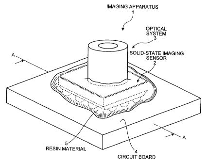
[0017] FIG. 1 is a schematic perspective view of an
example of a structure of an imaging apparatus according to
a first embodiment of the present invention;
FIG. 2 is a schematic cross-sectional view taken along
line A-A of FIG. 1;
FIG. 3 is an exemplary flowchart of manufacture of the
imaging apparatus according to the present invention;
FIG. 4 is a schematic perspective view of an example
of a structure of an imaging apparatus according to a
second embodiment of the present invention;
CA 02611916 2007-12-11
8
FIG. 5 is a schematic cross-sectional view taken along
line B-B of FIG. 4;
FIG. 6 is a schematic diagram showing a function of a
positioning unit that determines an attachment position of
an optical system;
FIG. 7 is a schematic perspective view of an example
of a structure of an imaging apparatus according to a
modified example of the second embodiment of the present
invention;
FIG. 8 is a schematic exemplary cross-sectional view
of a side section structure of a conventional imaging
apparatus; and
FIG. 9 is a schematic exemplary cross-sectional view
of a capsule endoscope incorporating the imaging apparatus
according to the first embodiment of the present invention.
EXPLANATIONS OF LETTERS OR NUMERALS
[0018] 1, 21 Imaging apparatus
2 Solid-state imaging sensor
2a CCD chip
2b Cover member
2c Electrode bosses
2d Light receiving unit
2e Rim
3, 23 Optical system
3a Lens
3b, 23b Barrel member
3c Through hole
3d Light receiving region
4 Circuit board
5 Resin material
23c, 23d Positioning unit
23e Engaging surface
CA 02611916 2007-12-11
9
101 Imaging apparatus
102 Solid-state imaging sensor
102a Light receiving unit
102b Cover glass
102c Solder balls
103 Optical system
103a Lens
103b Barrel member
103c Light blocking wall
103d Light receiving region
104 Circuit board
105 Resin material
201 Capsule endoscope
202 Casing
202a Optical dome
202b Dome
203 Light source
205 Transmitter
206 Transmitting antenna
207 Power source unit
BEST MODE(S) FOR CARRYING OUT THE INVENTION
[0019] Exemplary embodiments of an imaging apparatus and
a method of manufacturing the imaging apparatus according
to the present invention will be described in detail with
reference to the accompanying drawings. The present
invention is not limited to the embodiments.
[0020] First Embodiment
FIG. 1 is a perspective view schematically showing an
example of a structure of an imaging apparatus according to
a first embodiment of the present invention. As shown in
FIG. 1, an imaging apparatus 1 includes a solid-state
imaging sensor 2, an optical system 3, a circuit board 4,
CA 02611916 2007-12-11
and a resin material S. The solid-state imaging sensor 2
receives light from an object and performs photoelectric
conversion on the received light to acquire an image of the
object. The optical system 2 focuses the light from the
5 object on a light receiving surface of the solid-state
imaging sensor 2. The solid-state imaging sensor 2 is
mounted on the circuit board 4. The resin material 5
reinforces a packaging strength of the solid-state imaging
sensor 2 and the circuit board 4. The resin material 5
10 shields a region other than a light receiving region
(described later) of the solid-state imaging sensor 2 from
light.
[0021] Specifically, the solid-state imaging sensor 2 is
packaged as the CSP. The optical system 2 is arranged on
an upper surface of the solid-state imaging sensor 2. A
lower surface of the solid-state imaging sensor 2 is
attached to the circuit board 4. The solid-state imaging
sensor 2 mounted on the circuit board 4 is covered by the
resin material 5 so that only a region where the optical
system 3 is arranged is exposed (i.e., so that a region
other the light receiving region of the solid-state imaging
sensor 2 is covered). The resin material 5 fills up a
space between the solid-state imaging sensor 2 and the
circuit board 4.
[0022] FIG. 2 is an exemplary schematic cross-sectional
view of a side section structure of the imaging apparatus
shown in FIG. 1. As shown in FIG. 2, the solid-state
imaging sensor 2 includes a CCD chip 2a, a cover member 2b,
and electrode bosses 2c. The CCD chip 2a has a function of
acquiring an image of the object by receiving the light
from the object by the light receiving unit 2d and
performing photoelectric conversion. The cover member 2b
protects an upper surface of the CCD chip 2a, i.e., a
CA 02611916 2007-12-11
11
surface on which the light receiving unit 2d is formed.
The electrode bosses 2c serves to electrically connect the
CCD chip 2a and the circuit board 4 and to physically join
(in other words, mount) the CCD chip 2a on the circuit
board 4.
[0023] The CCD chip 2a is a semiconductor chip which has
a function of receiving the light from the object through
the light receiving surface and performing photoelectric
conversion on the received light to acquire an image of the
object. The CCD chip 2a has the light receiving unit 2d at
the upper surface side. The light receiving unit 2d
includes plural pixels each including a photoelectric
transducer. The light receiving unit 2d receives the light
from the object through the light receiving surface and
performs photoelectric conversion on the received light to
generate an electric signal corresponding to the image of
the object (image signal). Each side (vertical or
horizontal) of the rectangular CCD chip 2a is approximately
1 to 10 mm in length, and thickness of the CCD chip 2a is
approximately 0.1 to 0.5 mm.
[0024] The cover member 2b serves to protect the CCD
chip 2a without obstructing the reception of the light from
the object by the light receiving unit 2d. Specifically,
the cover member 2b is a translucent member made of
translucent glass, resin, or the like, and made to stick to
the upper surface of the CCD chip 2a, i.e., a side the
light receiving unit 2d is formed. The cover member 2b
protects the CCD 2a, and the light receiving unit 2d in
particular. An outer dimension of the cover member 2b
corresponds to the dimension of the rectangular CCD chip 2a
described above. Each side (vertical or horizontal) of the
rectangular cover member 2b is approximately 1 to 10 mm,
and thickness of the cover member 2b is approximately 0.1
CA 02611916 2007-12-11
12
to 0.5 mm.
[0025] The electrode bosses 2c function as external
electrodes through which the CSP-type solid-state imaging
sensor 2 is mounted on the circuit board 4, and which
electrically connects the solid-state imaging apparatus 2
and the circuit board 4. Specifically, the electrode
bosses 2c is an external electrode made of plural solder
balls or gold bumps. The electrode bosses 2c are arranged
on a lower surface side of the CCD chip 2a, i.e., at the
back of the side of the light receiving unit 2d is formed.
Here, the electrode bosses 2c are arranged corresponding to
the arrangement of electrodes (not shown) of the circuit
board 4. For example, the electrode bosses 2c are arranged
like a matrix on the lower surface of the CCD 2a.
Contrarily, the electrodes of the circuit board 4 may be
arranged corresponding to the arrangement of the electrode
bosses 2c. The electrode bosses 2c are subjected to a
heating treatment of not less than a predetermined
temperature, melted, and joined with the electrodes of the
circuit board 4. Thus, the solid-state imaging sensor 2
(more specifically, CCD chip 2a) is mounted on the circuit
board 4 via the electrode bosses 2c.
[0026] The optical system 3 includes a lens 3a that
focuses light from the object on the light receiving unit
2d, and a barrel member 3b that holds the lens 3a. The
lens 3a makes the light from the object pass through the
barrel member 3b, and focuses the light from the object on
the light receiving unit 2d to form an image. Here, the
lens in the optical system 3 may be a single lens 3a as
shown in FIG. 2; alternatively the lens may be a
combination of plural lenses.
[0027] The barrel member 3b is a cylindrical member in
which a through hole 3c is formed. An opening at one end
CA 02611916 2007-12-11
13
of the through hole 3c is closed holding the lens 3a. The
barrel member 3b is arranged on an upper surface of the
solid-state imaging sensor 2 (specifically, on the upper
surface of the cover member 2b) as shown in FIG. 2. The
barrel member 3b delineates a light receiving region 3d on
the surface of the cover member 2b at a position
corresponding to the position of the light receiving unit
2d. The barrel member 3b serves to keep the lens 3a and
the light receiving unit 2d at a fixed distance from each
other to allow an acquisition of a desired optical image.
The light receiving region 3d is a region on the surface of
the cover member 2b, and the light from the object coming
into the through hole 3c through the lens 3a passes through
the light receiving region 3d before being focused on the
light receiving unit 2d. The barrel member 3b functions so
as to make the light from the object coming into the
through hole 3c through the lens 3a reach the light
receiving region 3d, and to block external light incident
on the casing of the barrel member 3b (more specifically,
external light other than the light from the object).
[0028] The circuit board 4 is fabricated as a plate-like
printed circuit board or a flexible circuit board, or a
combination of both. Specifically, an electrode and
circuit wiring are formed on the circuit board 4 and the
solid-state imaging sensor 2 is mounted via the electrode
bosses 2c as described above. Further, various devices
(not shown) other than the solid-state imaging sensor 2 are
mounted on the circuit board 4 as necessary. For example,
an image processing device may be mounted for performing a
predetermined image processing on an image signal output
from the solid-state imaging sensor 2 to configure the
image of the object.
[0029] The resin material 5 serves to reinforce the
CA 02611916 2007-12-11
28964-146
14
packaging strength of the solid-state imaging sensor 2 and
the circuit board 4, and to shield the region other than the
light receiving region 3d of the cover member 2b from the
light. Specifically, the resin material 5 is a sealing
resin that is employed in a sealing process of a
semiconductor element or an underfill agent that is employed
as a strengthening agent for a package of CSP-type or BGA-
type semiconductor element. For example, the resin material
5 is a black resin such as black epoxy-based resin,
silicone-based resin, or polyimide-based resin. The resin
material 5 fills up the gap between the CCD chip 2a of the
solid-state imaging sensor 2 mounted on the circuit board 4
and the circuit board 4 to reinforce the packaging strength
of the solid-state imaging sensor 2 and the circuit board 4.
At the same time, the resin material 5 covers a region other
than the light receiving region 3d of the cover member 2b
(specifically an upper surface and side surfaces of the
cover member other than the surface where the light
receiving region 3d is formed) and forms a light blocking
film. Such light blocking film shields the region other
than the light receiving region 3d of the cover member 2b
and prevents the external light other than the light from
the object from coming into the light receiving unit 2d
through the cover member 2b. The resin material 5 is
applied in a fluid state onto the solid-state imaging sensor
2 and the circuit board 4. Hence, regardless of the outer
shape of the solid-state imaging sensor 2, i.e., the CCD
chip 2a, and the outer shape of the cover member 2b, the
resin material 5 can form the above-described light blocking
film flexibly, and at the same time the resin material 5 can
reinforce the packaging strength of the solid-state imaging
sensor 2 and the circuit board 4.
[0030] The packaging strength of the solid-state imaging
CA 02611916 2007-12-11
sensor 2 and the circuit board 4 is an anchorage strength
of the solid-state imaging sensor 2 with respect to the
circuit board 4, for example, and includes a bonding
strength of the electrode bosses 2c to the circuit board 4
5 and a bonding strength of the electrode bosses 2c to the
CCD chip 2a. Since the optical system 3 is attached to the
solid-state imaging sensor 2 in the imaging apparatus of
the first embodiment, an overall height of the imaging
apparatus increases. When an external force is applied to
10 the optical system 3 (the barrel member 3b, for example),
stress may concentrate on a bonding portion between each of
the electrode bosses 2c and the circuit board 4, or a
bonding portion between the electrode bosses 2c and the CCD
chip 2a. Therefore, the packaging strength of the solid-
15 state imaging sensor 2 and the circuit board 4 is required
to be higher than packaging strength generally required for
an integrated circuit (IC) or large scale integrated
circuit (LSI). In the first embodiment, the resin material
5 is formed so as to fill up all the gaps between the CCD
chip 2a and the circuit board 4. The present invention,
however, is not limited to such a manner of resin material
formation. The resin material 5 may partially fill up the
gaps between the CCD chip 2a and the circuit board 4; or
the resin material 5 may not fill up the gap at all, as far
as a desirable packaging strength can be secured.
[0031] The imaging apparatus 1 with the above-described
structure receives light from the object through the lens
3a by the light receiving unit 2d, and performs
photoelectric conversion on the received light from the
object to generate an image signal of the object, thereby
performing the imaging process of the image of the object.
Here, the light from the object passes through the lens 3a
to come inside the barrel member 3. Thereafter the light
CA 02611916 2007-12-11
16
passes through the light receiving region 3d to be focused
onto the light receiving surface of the light receiving
unit 2d. The light receiving unit 2d receives the light
from the object thus focused on the light receiving surface,
and performs photoelectric conversion on the received light
from the object to generate the image signal of the object.
Then, the image signal of the object is subjected to a
predetermined image process by an image processing unit.
Thus, an image of the object is formed according to the
image signal. The external light other than the light from
the object does not reach the light receiving unit 2d
blocked by the barrel member 3b and the resin material S.
[0032] A method of manufacturing the imaging apparatus 1
of the first embodiment of the present invention will be
described. FIG. 3 is an exemplary flowchart of processes
for manufacturing the imaging apparatus 1. As shown in FIG.
3, the cover member 2b is arranged on the upper surface of
the CCD chip 2a. The electrode bosses 2c are arranged on
the lower surface of the CCD chip 2a. The CCD chip 2a is
turned into a CSP. Thus, the CSP-type solid-state imaging
sensor 2 is manufactured (step S101). The CCD chips 2a,
then, can be mounted on the circuit board 4.
[0033] Here, the cover member 2b and/or the electrode
bosses 2c may be arranged on the CCD chip 2a which is
formed as a semiconductor chip cut out from a silicon
wafer; alternatively the cover member 2b and/or the
electrode bosses 2c may be arranged on a CCD element in a
sate of silicon wafer (i.e., CCD element before cut out
from the silicon wafer), and the CCD chip 2a may be cut out
later therefrom so that each includes the cover member 2b
or the electrode bosses 2c.
[0034] Then, the electrode bosses 2c of the CSP-type
solid-state imaging sensor 2 manufactured in step S101 are
CA 02611916 2007-12-11
17
joined with an electrode of the circuit board 4 (step S102).
The electrode bosses 2c are brought into contact with the
electrode of the circuit board 4. Then, the electrode
bosses 2c are heated and melted while in contact with the
electrode of the circuit board 4. Thus the solid-state
imaging sensor 2 is mounted on the circuit board 4. The
solid-state imaging sensor 2 is fixed to the circuit board
4 by the melted electrode bosses 2c. The step 102 is not
limited to the manner mentioned above. The solid-state
imaging sensor 2 may be pressed onto the electrode of the
circuit board 4 while the electrode bosses 2c are melted
and adhered to the electrode of the circuit board 4.
Alternatively, ultrasonic waves may be applied to the
solid-state imaging sensor 2 and the circuit board 4 to
make the electrode bosses 2c melted and adhered.
[0035] Thereafter, the optical system 3 is arranged on
the cover member 2 of the solid-state imaging sensor 2
mounted on the circuit board 4 (step S103). The barrel
member 3b of the optical system 3 is arranged so that the
light receiving region 3d is formed on the surface of the
cover member 2b at a position corresponding to the light
receiving unit 2d. When the barrel member 3b is thus
arranged, the lens 3a is located over the light receiving
region 3d.
[0036] Then, the packaging strength of the solid-state
imaging sensor 2 and the circuit board 4 is reinforced by
the resin material 5, and at the same time, the resin
material 5 shields the region outside the light receiving
region 3d of the cover member 2b from light (step S104).
Specifically, the resin material 5 is poured into the gaps
between the mounted solid-state imaging sensor 2 (more
specifically the CCD chip 2a) and the circuit board 4,
thereby filling in the gaps and reinforcing the packaging
CA 02611916 2007-12-11
18
strength of the solid-state imaging sensor 2 and the
circuit board 4. At the same time, the resin material 5
covers the region outside the light receiving region 3d of
the cover member 2b to form the light blocking film. The
light blocking film shields the region outside the light
receiving region 3d from the light. Thus, the imaging
apparatus 1 as exemplified in FIGS. 1 and 2 is manufactured.
[0037] As described above, in the first embodiment of
the present invention, the gaps between the semiconductor
chip of the solid-state imaging sensor and the circuit
board is filled up by the light-blocking resin material,
whereby the packaging strength is reinforced and the light
blocking film is formed in the region outside the light
receiving region of the cover member (translucent member)
of the solid-state imaging sensor. Therefore, even when a
casing structure of the light blocking wall (e.g., the
light blocking wall 103c shown in FIG. 8) is not provided
in the optical system that focuses the light from the
object onto the light receiving surface of the solid-state
imaging sensor, the resin material forms the light blocking
film and shields the region outside the light receiving
region of the translucent member from the light without
fail. Further, a casing structure of the optical system
can be simplified, which enhances the versatility of the
optical system with respect to the outer dimension of the
solid-state imaging sensor. Still further, a degree of
freedom in positioning of the optical system with respect
to the solid-state imaging sensor can be increased.
Therefore, an imaging apparatus can be readily realized in
which the optical system that focuses light from the object
can be readily attached to the solid-state imaging sensor
and in which unnecessary external light other than the
light from the object can be surely blocked.
CA 02611916 2007-12-11
19
[0038] Further, since the resin material is applied in a
fluid state to the region outside the light receiving
region of the translucent member to form the light blocking
film, the light blocking film can be formed flexibly
regardless of the outer dimension and the size of the
solid-state imaging sensor, i.e., the outer dimension of
the translucent member, whereby the region outside the
light receiving region of the translucent member can be
surely shielded from light in the solid-state imaging
sensor of a desired outer dimension and size.
[0039] Since the imaging apparatus according to the
present invention in which the light blocking film is
formed of the resin material does not need the casing
structure of the light blocking wall as described above,
the scale of the imaging apparatus can be reduced, and
therefore the imaging apparatus of the present invention is
suitable as a small imaging apparatus to be incorporated
into digital camera, video camera, portable terminals such
as mobile telephone with a camera function, and PDA with a
camera function, and medical devices such as endoscope or
capsule endoscope that is employed for observation of
inside a subject, such as an inside of alimentary tracts of
a subject.
[0040] Second Embodiment
A second embodiment of the present invention will be
described. An imaging apparatus according to the second
embodiment further includes a positioning unit in a barrel
member of an optical system that is placed on an upper
surface of a solid-state imaging sensor. The positioning
unit determines an attachment position in the solid-state
imaging sensor.
[0041] FIG. 4 is a perspective view schematically
showing an example of a structure of the imaging apparatus
CA 02611916 2007-12-11
according to the second embodiment of the present invention.
FIG. 5 is a schematic cross-sectional view taken along line
B-B and schematically shows an exemplary side section
structure of the imaging apparatus shown in FIG. 4. As
5 shown in FIGS. 4 and 5, an imaging apparatus 21 includes an
optical system 23 in place of the optical system 3 of the
imaging apparatus 1 of the first embodiment described above.
Other structure of the second embodiment is the same as the
structure of the first embodiment and the same elements are
10 denoted by the same reference characters.
[0042] The optical system 23 includes the lens 3a, and a
barrel member 23b which has a positioning unit 23c
mentioned above at one end. The through hole 3c is formed
inside the barrel member 23b and an opening at one end of
15 the through hole 3c is closed by holding the lens 3a. The
barrel member 23b, similarly to the barrel member 3b
described above, delineates the light receiving region 3d
on the upper surface of the cover member 2b at a position
corresponding to the light receiving unit 2d.
20 [0043] The positioning unit 23c is formed at the end of
the barrel member 23b at the side of cover member 2b. The
positioning unit 23c is formed in a shape fittable to a rim
of the cover member 2b. For example, the positioning unit
23c has a substantially L-shaped sectional structure. The
positioning unit 23c is caught by the rim of the cover
member 2b, thereby restricting and determining the
attachment position of the optical system 23 (specifically,
the barrel member 23b) on the cover member 2b.
[0044] FIG. 6 is a schematic diagram showing a function
of the positioning unit 23c that determines the attachment
position of the optical system 23 on the upper surface of
the solid-state imaging sensor 2. As shown in FIG. 6, the
positioning unit 23c has an engaging surface 23e which is
CA 02611916 2007-12-11
21
provided at a side that is brought into contact with the
cover member 2b and is able to engage with a rim 2e of the
cover member 2d. The attachment position of the optical
system 23 having the positioning unit 23c on the cover
member 2b is determined by the engagement of the engaging
surface 23e and the rim 2e when the optical system 23 is
placed on the upper surface of the cover member 2b. When
the optical system 23 (more specifically the barrel member
23b) is fixed onto the cover member 2b at the attachment
position determined as described above, the opening of the
through hole 3c can be readily aligned with the light
receiving region 3d with high accuracy.
[0045] The imaging apparatus 21 with the above described
structure can be manufactured by sequentially conducting
the processes of S101 to S104 of the first embodiment. In
the step of arranging the optical system 23 on the upper
surface of the solid-state imaging sensor 2 (step S103), an
optimal attachment position of the optical system 23 can be
readily determined by the positioning unit 23c, whereby the
optical system 23 can be fixed onto the cover member 2b
while the opening of the through hole 3c is aligned with
the light receiving region 3d with high accuracy.
[0046] As described above, according to the second
embodiment of the present invention, the imaging apparatus
can be provided in which: the imaging apparatus has the
structure of the first embodiment; the positioning unit is
formed in the barrel member of the optical system to
determine the attachment position of the optical system on
the upper surface of the solid-state imaging sensor; the
optimal attachment position of the optical system can be
readily determined by the positioning unit when the optical
system is attached to the solid-state imaging sensor;
advantages of the first embodiment can be enjoyed; and the
CA 02611916 2007-12-11
22
light receiving region, i.e., the region on the cover
member (translucent member) corresponding to the light
receiving surface of the solid-state imaging sensor can be
readily aligned with the opening of the through hole of the
optical system with high accuracy.
[0047] Third Embodiment
A third embodiment of the present invention will be
described. The third embodiment provides a capsule
endoscope incorporating the imaging apparatus 1 of the
first embodiment inside a capsule-like casing.
[0048] FIG. 9 is a schematic cross-sectional view of the
capsule endoscope incorporating the imaging apparatus 1 of
the first embodiment of the present invention. As shown in
FIG. 9, a capsule endoscope 201 has a capsule-like casing
202 which has a substantially cylindrical shape. The
casing 202 includes an optical dome 202a formed of a
transparent optical member on one end and an opaque dome
202b on another end. Further, the capsule endoscope 201
includes inside the casing 202 an imaging mechanism which
images inside a body cavity to obtain image data, a radio
mechanism which sends various types of information
including the image data, and a power supply unit 207.
[0049] The imaging mechanism of the capsule endoscope
201 is arranged in the vicinity of the optical dome 202a.
The imaging mechanism includes light sources 203 and the
imaging apparatus 1. The light source 203 consists of a
light emitting element such as a light emitting diode (LED)
and illuminates an examined region inside the body cavity
of a subject (not shown) through the optical dome 202a.
The examined region in the body cavity illuminated with the
light source 203 reflects the light. The imaging apparatus
1 receives the reflected light from the examined region
inside the body cavity to obtain an image thereof. The
CA 02611916 2007-12-11
23
imaging apparatus 1 includes the solid-state imaging sensor
2, the optical system 3, the circuit board 4, and the resin
material 5 as described above. Here, the optical system 3
focuses the light that is reflected from the examined
region inside the body cavity and enters through the
optical dome 202a on the solid-state image sensor 2. The
solid-state imaging sensor 2 obtains an image of the
examined region inside the body cavity based on the
reflected light focused by the optical system 3. The
circuit board 4 sends an image signal corresponding to the
obtained image to the radio mechanism of the capsule
endoscope 201. Here, two light sources 203 are provided
around the imaging apparatus 1 in FIG. 9. The number of
light sources, however, is not limited to two, and may be
one, three, or more.
[0050] The radio mechanism of the capsule endoscope 201
is provided near and inside the dome 202b. The radio
mechanism includes a transmitter 205 and a transmitting
antenna 206. The transmitter 205 modulates the image
signal sent from the imaging apparatus linto an RF signal.
The transmitting antenna 206 transmits electric waves of
the RF signal generated by the transmitter 205 to a
receiver (not shown) outside the subject. In other words,
the transmitter 205 generates the RF signal and sends the
RF signal to the receiver outside the subject using the
transmitting antenna 206. The RF signal includes image
data of the examined region inside the body cavity. The
image data is obtained by the imaging apparatus 1.
[0051] The power source unit 207 supplies driving power
to the imaging apparatus 1, the light sources 203, the
transmitter 205, and the transmitting antenna 206. The
capsule endoscope 201 may further include a receiver and a
receiving antenna in order to receive various control
CA 02611916 2007-12-11
24
signals transmitted by predetermined electric waves by an
external device (not shown) and to control driving of the
light sources 203, the imaging apparatus 1, or the like
based on the received control signals.
[0052] In the capsule endoscope 201 with the above
described structure which houses the imaging apparatus 1
inside the casing 202, the imaging apparatus 1 is formed to
an ultrasmall size. Therefore, the casing 202 can be
further downsized, which leads to further downsizing of the
capsule endoscope. In addition, when such imaging
apparatus 1 is incorporated, some space may remain in the
casing where other mechanism can be arranged without
enlargement of the casing 202. Therefore, additional
mechanism for diagnosis, treatment, or the like, can be
arranged in the capsule endoscope 201 as necessary.
[0053] In the first and the second embodiments of the
present invention, the CCD chip 2a is employed as a
semiconductor chip having an imaging function of the solid-
state imaging sensor 2. The present invention, however, is
not limited to the CCD chip. A CMOS chip may be employed
in place of the CCD chip 2a and the solid-state imaging
sensor 2 may be a CMOS image sensor.
[0054] Further, in the first and the second embodiments,
the solid-state imaging sensor 2 is packaged as a CSP. The
present invention, however, is not limited to such
packaging manner. The solid-state imaging sensor may be
packaged as a BGA (Ball Grid Array) package, or a LCC
(Leadless Chip Carrier) package. Further, any packaging
manner may be adaptable which implements the semiconductor
chip of the solid-state imaging sensor and the circuit
board by a flip chip connection.
[0055] Further, in the first and the second embodiments,
the solid-state imaging sensor is mounted on the circuit
CA 02611916 2007-12-11
board (step S102) and thereafter the optical system is
arranged on the upper surface of the solid-state imaging
sensor (step S103). The present invention, however, is not
limited to the order of processes as described above. It
5 is possible to arrange the optical system on the upper
surface of the solid-state imaging sensor, and to mount the
solid-state imaging sensor on the circuit board thereafter.
In this case, the step S101 of manufacturing the imaging
sensor is followed by the step S103 of arranging the
10 optical system, and further by the step S102 of joining.
After the processes from S101 to S103 are carried out in
the order as described above, the step S104 of
reinforcement and light blocking is performed. Thus, the
imaging apparatus of the present invention can be
15 manufactured.
[0056] In the second embodiment, one positioning unit is
formed in the barrel member of the optical system. The
present invention, however, is not limited to one
positioning unit. There may be plural positioning units in
20 the barrel member of the optical system. FIG. 7 is a
perspective view schematically showing an example of a
structure of a modified example of the imaging apparatus 21
of the second embodiment of the present invention. In FIG.
7, the resin material 5 is not shown in order to clearly
25 show plural positioning units. The optical system 23 of
the imaging apparatus as the modified example has plural
positioning units 23c and 23d corresponding respectively to
two sides that run at right angles to one another of the
cover member 2b, for example as shown in FIG. 7. The
positioning unit 23d is formed in a shape fittable with a
rim of the cover member 2b similarly to the positioning
unit 23c. The positioning units 23c and 23d engage
respectively with the rims of the cover member 2b when the
CA 02611916 2007-12-11
26
optical system 23 is arranged on the upper surface of the
solid-state imaging sensor 2, whereby the attachment
position of the optical system 23 can be determined in
widthwise and lengthwise directions of the upper surface of
the cover member 2b. Thus, the optical system 23 can be
securely arranged at an optimal attachment position.
[0057] In the third embodiment, the capsule endoscope
201 incorporates the imaging apparatus 1 according to the
first embodiment. The present invention, however, is not
limited to such a structure. The capsule endoscope 201 may
incorporate the imaging apparatus 21 according to the
second embodiment in place of the imaging apparatus 1 of
the first embodiment.
[0058] In the third embodiment, the capsule endoscope
201 incorporate the imaging apparatus 1 of the first
embodiment. The present invention, however, is not limited
to such a structure. The imaging apparatus 1 or the
imaging apparatus 21 of the present invention may be
incorporated into capsule endoscope, endoscope, digital
camera, and portable terminal having a camera function such
as mobile telephone, and PDA. Devices incorporating the
imaging apparatus 1 or the imaging apparatus 21 enjoy the
advantages of the third embodiment described above.
INDUSTRIAL APPLICABILITY
[0059] The imaging apparatus of the present invention is
useful for downsizing of various devices with imaging
function. In particular, the imaging apparatus of the
present invention is suitable for a small imaging apparatus
incorporated in digital camera, video camera, portable
terminals with camera function such as mobile telephone and
PDA, medical devices such as endoscope or capsule endoscope
employed for observation of alimentary tracts or the like
CA 02611916 2007-12-11
27
of a subject. The method of manufacturing the imaging
apparatus according to the present invention is useful as
manufacturing method that enhances versatility of an
optical system attached to a solid-state imaging sensor and
readily realizes such a small imaging apparatus.
Fetherstonhaugh
Ottawa, Canada
Patent Agents