Note: Descriptions are shown in the official language in which they were submitted.
CA 02611923 2007-12-12
WO 2006/136645 PCT/F12005/050237
1
Simulation of multi-antenna radio channel
Field
The invention relates to a device for simulating a multi-antenna ra-
dio channel, a channel module for simulating a multi-antenna radio channel,
and a method of simulating a multi-antenna radio channel.
Background
A simulation of multi-antenna radio channels, such as MIMO (Multi-
ple Input, Multiple Output) radio channels, involves a simulation of
propagation
of a radio signal through a radio sub-channel between transmit antennas and
receive antennas. In a typical radio channel simulator, each radio sub-channel
is simulated in a radio channel unit. Typically, the radio channel units are
pre-
ceded by a pre-router, which switches antenna signals to an appropriate radio
channel unit. Signals outputted by the radio channel units are fed into a post-
router, which combines the signals and routes the signals to appropriate
output
channels.
Routing and combining routines, however, involve external wiring
which is prone to failure, and a complex switching matrices and adders. There-
fore, it is useful to consider more advanced techniques for simulating multi-
antenna radio channels.
Brief description of the invention
An object of the invention is to provide an improved device, module
and method. According to a first aspect of the invention, there is provided a
device for simulating a multi-antenna radio channel, the device comprising
channel modules for incorporating propagation effects into channel signals
which represent radio signals propagating along propagation paths, which
channel modules are electrically connected to neighbour channel modules for
forming an (m,n) array configuration, at least one (m,n)th channel module
being
configured to receive a first (m,n-1)th channel signal and a second (m-1,n)tn
channel signal, the at least one (m,n)th channel module comprising: at least
one processing resource for processing the first (m,n-1)th channel signal ac-
cording to a channel model, thus generating a processed (m,n)th channel sig-
nal; and a combiner for combining the processed (m,n)th signal and the second
(m-1,n)th channel signal, thus generating a second (m,n)th channel signal, the
CA 02611923 2007-12-12
WO 2006/136645 PCT/F12005/050237
2
at least one (m,n)th channel module further being configured to output the seG
ond (m,n)th channel signal.
According to a second aspect of the invention, there is provided a
channel module for simulating a multi-antenna radio channel, the channel
module being configured to be electrically connectable to neighbour channel
modules in an (m,n) array configuration, the channel module being configured
to receive a first (m,n-1 )th channel signal and a second (m-1,n)th channel
sig-
nal, the channel module comprising: at least one processing resource for proc-
essing the first (m,n-1)th channel signal according to a channel model, thus
generating a processed (m,n)th channel signal; and a combiner for combining
the processed (m,n)th signal and the second (m-1,n)th channel signal, thus
generating a second (m,n)th channel signal, the channel module further being
configured to output the second (m,n)th channel signal.
According to another aspect of the invention, there is provided a
method of simulating a multi-antenna radio channel, the method comprising:
receiving a first (m,n-1 )th channel signal and a second (m-1,n)th channel
signal
at an (m,n)th channel module electrically connected to neighbour channel mod-
ules configured into an array configuration; generating a processed (m,n)tn
channel signal by processing the first (m,n-1)th channel signal according to a
channel model; combining the processed (m,n)th channel signal and the sec-
ond (m-1,n)th channel signal, thus generating a second (m,n)th channel signal;
and outputting the second (m,n)th channel signal.
The invention provides several advantages. Routing of channel sig-
nals propagating in a radio channel simulator is realized locally by electric
con-
nections and an array structure of channel modules which incorporate propa-
gation effects into the channel signals. Local routing reduces a need for com-
plex routing and switching systems, thus simplifying the structure of a radio
channel simulator. In an embodiment, the invention further enables a radio
channel simulator to be implemented with a modular structure, which is easily
expandable.
List of drawings
In the following, the invention will be described in greater detail with
reference to the embodiments and the accompanying drawings, in which
Figure 1 illustrates a signal propagation environment typical of radio
systems;
CA 02611923 2007-12-12
WO 2006/136645 PCT/F12005/050237
3
Figure 2 illustrates an exemplified channel model by means of a
block diagram;
Figure 3 shows an example of a structure of a device for simulating
a multi-antenna radio channel;
Figure 4A illustrates a structure of a simulation array;
Figure 4B illustrates a structure of a simulation array;
Figure 5 shows a first example of a channel module;
Figure 6 shows a second example of a channel module;
Figure 7 shows a third example of a channel module;
Figure 8 shows another example of a channel module;
Figure 9 shows a first example of an implementation of a simulation
array;
Figure 10 shows a second example of an implementation of a simu-
lation array; and
Figure 11 illustrates a methodology according to embodiments of
the invention.
Description of embodiments
Figure 1 illustrates a propagation channel 114 formed by a transmit
receive-antenna pair, which comprises a transmit antenna 100 and a receive
antenna 102. A transmit signal 116 is inputted into the transmit antenna 100,
which converts the transmit signal 116 into an electromagnetic wave 120. A
portion of the electromagnetic wave 120 propagates to the receive antenna
102, which converts the portion of the electromagnetic wave 120 into a receive
signal 118.
The propagation channel 114 includes at least one propagation path
104, 106 for the electromagnetic wave 120. The propagation paths 104, 106
represent different routes of the electromagnetic wave 120 from the transmit
antenna 100 to the receive antenna 118. The propagation paths 104, 106 typi-
cally represent routes which provide the most favourable propagation effects
for the electromagnetic wave 120 in terms of the receive power of the electro-
magnetic wave 120 in the receive antenna 102. Each propagation path 104,
106 may have its characteristic propagation effects on the electromagnetic
wave 120.
In a radio system, the electromagnetic wave 120 carries information
from the transmit antenna 100 to the receive antenna 102. In multi-path propa-
gation, the propagation channel 114 includes a plurality of propagation paths
CA 02611923 2007-12-12
WO 2006/136645 PCT/F12005/050237
4
104, 106. Typically, the amplitude of the receive signal 118 is a vector sum
of
the multi-path components of the electromagnetic field 120.
While propagating from the transmit antenna 100 to the receive an-
tenna 102, the electromagnetic wave 120 is subjected to propagation effects,
such as attenuation, absorption, reflection, scattering, diffraction, and
refrac-
tion. Some of the propagation effects, such as absorption, reflection, scatter-
ing, diffraction, and refraction, may be caused by obstructions 108, 110, 112
encountered by the electromagnetic wave 120. Some of the obstructions 108,
110, 112 may move relative to the transmit antenna 100 and/or receive an-
tenna 102. Typically, attenuation arises from a reduction in the power of the
electromagnetic wave 120 as a function of the physical length of a propagation
path 104, 106. In terms of characteristics of the electromagnetic wave 120,
the
propagation effects may affect the amplitude, phase and frequency of the elec-
tromagnetic wave 120.
Furthermore, the electromagnetic wave 120 may be interfered by
other signal sources, such as radio transmitters, and thermal noise.
The propagation channel 114 further depends on the characteristics
of the transmit antenna 100 and the receive antenna 102. The wave front as-
sociated with the electromagnetic wave 120 depends on the type of the trans-
mit antenna 100. Furthermore, sampling of the portions of the electromagnetic
wave 120 arriving at the receive antenna 102 depends on the type of the re-
ceive antenna 102. Therefore, the antenna characteristics of the transmit an-
tenna 100 and the receive antenna 102 are preferably taken into account in a
radio channel simulation.
It is noted that the exemplified propagation channel 114 shown in
Figure 1 illustrates a case wherein one transmit antenna 100 and one receive
antenna 102 are applied. In the case of multi-antenna radio channels, at least
three antennas are used for forming a radio channel. Each transmit-receive
antenna pair forms an antenna-pair-specific propagation channel with antenna-
pair-specific propagation paths.
Typically, a radio channel simulation is based on a channel model
characterizing the propagation channels. Figure 2 shows a block diagram rep-
resentation of a radio channel and the associated radio channel parameters.
The exemplified radio channel shown in Figure 2 is a MIMO (Multiple-Input
Multiple-Output), which is formed by using at least two transmit antennas 206,
208 and at least two receive antennas 210, 212.
CA 02611923 2007-12-12
WO 2006/136645 PCT/F12005/050237
A radio channel simulation may be performed between two trans-
ceivers, such as a base transceiver station and a mobile station, of a
wireless
telecommunications system. The invention is not, however, restricted to tele-
communications system, but may be applied to any system applying at least
5 three antennas in forming a radio channel.
It is clear to a person skilled in the art how to apply teachings learnt
from a MIMO channel to simpler systems, such as MISO (Multiple-Input Sin-
gle-Output) and SIMO (Single-Input Multiple-Output).
Figure 2 shows a transmitter 200 connected to transmit antennas
206, 208, a receiver 202 connected to receive antennas 210, 212, and a radio
channel 204 including the effects from the propagation paths 104, 106 and the
antennas 208 to 212.
The transmitter 200 inputs transmit signals 220A and 220B into the
transmit antennas 206 and 208, respectively. The receiver 202 receives a por-
tion of the electromagnetic wave produced by the transmit antennas 206, 208
and outputs receive signals 222A and 222B from the receive antennas 210
and 212, respectively.
Figure 2 further shows propagation channels 214, 216, 218, and
220.
In an embodiment, the radio channel 204 may be characterized us-
ing a channel equation
hll ... h1M x1
LY1 ... YNI
, (1 )
hNl ... hNM xM
wherein vector component Xk (k=1,..,M) of the transmit signal vector
represents
a transmit signal directed at the kth transmit antenna, vector component of
the
receive signal vector yj (j=1,..,N) represents a receive signal outputted by
the jtn
receive antenna, and coefficient hkj represents the portion of the radio
channel
associated with the kth transmit antenna and the jth receive antenna. The chan-
nel coefficients may also be called a channel tap and/or an impulse response.
In a wideband channel with bandwidth B, the channel taps may further charaG
terize the frequency response of the propagation channel.
The temporal variation of the radio channel and a multi-path
propagation may be accounted for by writing
h4 (t) = h4 (hl (t), ..,h' (t),..,h' (t)) (2)
y; (t) = y; (v~ (t), ==,y~ (t),==,y~ (t)) (3)
CA 02611923 2007-12-12
WO 2006/136645 PCT/F12005/050237
6
wherein superscript I refers to an Ith propagation path. Each propagation path
I
may be associated with a propagation-path-specific channel coefficient h'(t)
and a receive signal y. (t). The channel coefficient h'(t) and the receive sig-
nal y. (t) may have or may not have a time dependence. The channel coeffi-
cients h' (t) are typically complex variables.
With reference to an example shown in Figure 3, a device 300 for
simulating a multi-antenna radio channel typically includes an input radio fre-
quency domain (IRFD) 302, which receives radio frequency input signals 312
and converts the radio frequency input signals 312 into baseband input signals
314.
The radio frequency input signals 312 may be transmit radio fre-
quency antenna signals, such as MIMO transmit signals, generated in a device
representing a radio transmitter, such as a base station or a mobile station,
for
example.
The baseband input signals 314 are inputted into a pre-processing
unit (PRPU) 304, which is responsible for tasks such as scaling, packetizing,
time sharing, frequency division and/or IQ-division of the baseband input sig-
nals 314.
The pre-processing unit 304 outputs channel signals 316 which rep-
resent radio signals entering into propagation paths 104, 106 to be simulated.
The channel signals 316 are inputted into a simulation array (SA)
306, which incorporates propagation effects of the multi-antenna radio channel
into channel signals 316. The propagation of channel signals in the multi-
antenna radio channel is simulated by subjecting the channel signals to chains
of mathematical operations.
In an embodiment of the invention, the simulation array 306 is used
for simulating an MxN MIMO radio channel provided by M transmit antennas
and N receive antennas. In such a case, each column of the simulation matrix
simulates an Mxl portion of the simulation.
The simulation array 306 outputs channel signals 318, which repre-
sent radio signals exiting the propagation paths 104, 106.
The channel signals 318 are inputted into a post-processing unit
(POPU) 308, which processes the channel signals 318 by, for example, by
combining the channel signals 318.
CA 02611923 2007-12-12
WO 2006/136645 PCT/F12005/050237
7
The post-processing unit 308 outputs baseband output signals 320
into an output radio frequency domain (ORFD) 310, which converts the base-
band output signals 320 into radio frequency output signals 322. The radio fre-
quency output signals may be MIMO receive signals, for example.
The device 300 may further comprise a controller 324 for controlling
the functional blocks 302 to 310 of the device 300. A control may include
tasks
such as synchronizing bit flows in the device 300, programming the channel
modules of the simulation array 306 according to the channel model, and con-
trol of input/output traffic.
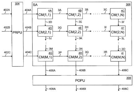
With reference to Figure 4A, the simulation array 306 comprises
channel modules (CM) 4A to 41 which incorporate propagation effects into
channel signals 404A to 404C, 3A to 3R representing radio signals propagat-
ing along propagation paths 104, 106. The channel modules 4A to 41 are elec-
trically connected in an (m,n) array configuration, where each (m,n)th channel
module is electrically connected to neighbour (m,n)th channel modules. In the
notation adopted, each (m,n)th channel module is associated with different
(m,n) indices such that m and n indicate rows and columns, respectively, of
the
simulation array 306.
A channel signal 404A to 404C, 3A to 3R may involve 32 bits trans-
ported over a parallel bus. The channel signal 404A to 404C, 3A to 3R may
include 16 bits dedicated to a Q component and 16 bits dedicated to an I com-
ponent. The clock frequency of the data transport may be 200 MHz, for exam-
ple.
The dimensions of the simulation array 306 are M and N, where M
and N are the maximum of m and n, respectively.
The channel signals 404A to 404C, 3A to 3R are identified with
(m,n) labels. A first (m,n)th channel signal 404A to 404C, 3A to 3C, 3G to 31,
3P
to 3R is a channel signal generated in an (m,n)th channel module and/or the
pre-processing unit 304 and received by an (m,n+1)th channel module. The
first (m,n)th channel signals 404A to 404C, 3A to 3C, 3Gto 31, 3P to 3R propa-
gate in the horizontal direction in the simulation array 306.
A second (m,n)th channel signal 406A to 406C, 3D to 3F, 3J to 3L,
3M to 30 is a channel signal outputted by an (m,n)th channel module and re-
ceived by an (m+1,n)th channel module or the post-processing unit 308. The
second (m,n)th channel signals 406A to 406C, 3D to 3F, 3J to 3L, 3M to 30
propagate in the vertical direction in the simulation array 306.
CA 02611923 2007-12-12
WO 2006/136645 PCT/F12005/050237
8
Channel signals 404A to 404C outputted by the pre-processing unit
304 are denoted by (m,n=0). In terms of the channel equation (1), the channel
signals 404A to 404C outputted by the pre-processing unit 304 may represent
xm components of the column vector of the right-hand side of equation (1).
Channel signals 406A to 406C outputted by the simulation array
306 are denoted by (M,n). In terms of the channel equation (1), the channel
signals 406A to 406C outputted by the simulation array 306 may represent yn
components of the vector of the left-hand side of equation (1).
The pre-processing unit 304 may be provided with a plurality of
baseband input signals 402A to 402C which may represent transmit antenna
signals in the base band domain. In an embodiment of the invention, the pre-
processing unit 304 is capable of routing each baseband input signal 402A to
402C into any (m,n=1)th channel module 4A, 4D, 4G. Routing may be imple-
mented with switches controlled by the controller 324.
In an embodiment of the invention, the post-processing unit 308 is
capable of converting any (m=M,n)th channel signal 406A to 406C to any base
band output signal 408A to 408C. A conversion may be implemented with
switches controlled by the controller 324. The post-processing unit 308 may
further comprise a combiner, such as an adder, for combining at least two
(m=M,n)th channel signals 406A to 406C into a single baseband output signal
408A to 408C.
With reference to Figure 4B, let us consider a simulation array 410
capable of simulating a 4x4 MIMO system.
In this case, the pre-processing unit 304 receives four baseband in-
put signals 402A to 402D and inputs four channel signals 404A to 404D into
the simulation array 410. The simulation array 410 routes and processes the
channel signals and outputs four channel signals 406A to 406D to the post-
processing unit 308. The post-processing unit 308 receives the four channel
signals 406A to 406D and outputs four baseband output signals 408A to 408D.
In this case, each column of the simulation array is used for simulating a 4x1
MIMO sub-channel.
The routing and conversion enabled by the pre-processing unit 304
and the post-processing unit 308 make it possible to allocate processing power
to desired sub-channels. For example, the 4x4 simulation array 410 may be
used for simulating a 4x3 MIMO system by combining channel signals 406A
CA 02611923 2007-12-12
WO 2006/136645 PCT/F12005/050237
9
and 406B into a single baseband output signal 408A. In this case, columns
inside a dotted rectangle are allocated to one of the 1x3 MIMO sub-channels.
If the bandwidth of the radio signal being simulated is narrow, a sin-
gle channel module 5A to 5P may be used for simulating a plurality of sub-
channels. In terms of the channel model of Equation (1), a single channel
module 5A to 5P implements more than one hmn channel taps. The sub-
channels may be simulated by time-multiplexing the channel module between
the sub-channels.
With reference to Figure 5, an (m,n)th channel module 500 com-
prises a processing resource (PR) 502 and a combiner (COMB) 504 con-
nected to the processing resource 502.
The processing resource 502 receives a first (m,n-1)th channel sig-
nal 508 from the (m,n-1 )th channel module or from the pre-processing unit 304
and processes the first (m,n-1)th channel signal 508 according to the channel
model being applied to a radio channel simulation. As a result of processing,
a
processed (m,n)th channel signal 514 is obtained. In terms of the channel
equation (1), the (m,n)th channel module may implement an hmn(t) channel tap
shown in equation (2).
The processing resource 502 inputs the processed (m,n)th channel
signal 514 into the combiner 504 which combines the processed (m,n)th chan-
nel signal 514 with a second (m-1,n)th channel signal 506 received from a(m-
1,n)th channel module, thus resulting in a second (m,n)th channel signal 512.
The combiner 504 outputs the second (m,n)th channel signal 512 into an
(m+1,n)th channel module or into the post-processing unit 308.
Each channel module in a same row of the simulation array 306 is
provided with a same first channel signal. For example, channel signals 3A to
3C equal channel signal 404A, channel signals 3G to 31 equal channel signal
404B and channel signals 3P to 3R equal channel signal 404C.
In an embodiment of the invention, the channel modules in the
same row are electrically connected with the neighbour channel modules via
an external connection. The external connection may be provided by a printed
board or another structure onto which the channel modules 4A to 41 are at-
tached.
In an embodiment of the invention, the (m,n)th channel module 500
is configured to output the first (m,n-1)th channel signal 508 as a first
(m,n)tn
channel signal 510, thus enabling local routing of the horizontal signals in
the
CA 02611923 2007-12-12
WO 2006/136645 PCT/F12005/050237
simulation array 306. The local routing may be implemented by connecting an
input bus of the first (m,n-1 )th channel signal 510 to the output bus of the
first
(m,n)th channel signal 510.
The combiner 504 may be an adder or a multiplier, for example.
5 In an embodiment of the invention, the channel modules 4A to 41 of
the simulation array 306 are identical with each other, comprising the process-
ing resource 502 and the combiner 504. The uppermost channel modules 4A
to 4C denoted by (m=1,n) may be provided with zero bits as second (m=0,n)tn
channel signals. The zero bits may be generated in the uppermost channel
10 modules 4A to 4C.
With reference to Figure 6, in an embodiment of the invention, an
(m=1,n)th channel module 600 is configured to receive a first (m=1,n-1)th chan-
nel signal 602. The (m=1,n)th channel module 600 corresponds to a channel
module 4A to 4C of Figure 4A, for example. The (m=1,n)th channel module 600
comprises at least one processing resource 502 for incorporating the propaga-
tion effect into the first (m=1,n-1)th channel signal 602, thus generating a
seG
ond (m=1,n)th channel signal 604. The (m=1,n)th channel module 600 further
outputs the second (m=1,n)th channel signal 604.
The channel module 600 may bypass the first (m=1,n)th channel
signal 602 and output the first (m=1,n+1)th channel signal 606.
With reference to Figure 7, an (m,n)th channel module 700 may
comprise K delay elements 704A to 704C, K multipliers 706A to 706C and an
adder 708. Delay lengths of the delay elements 704A, 704B and 704C are rep-
resented by til, ti2, tiK respectively. Multiplying coefficients of the
multipliers
706A, 706B and 706C are represented by gi, 92 and gK, respectively. Values
of the delay lengths and multiplying coefficients may be varied according to
control of the controller 324, for example. Furthermore, relative positions of
the
delay elements 704A to 704C and those of the multipliers 706A to 706C may
be controlled by switches not shown in Figure 7. A switch configuration may be
controlled by the controller 324.
In Figure 7, the delay element 704A and the multiplier 706A provide
a representation of a first propagation path, the delay element 704B and the
multiplier 706B of a second propagation path, and the delay element 704C and
the multiplier 706C of a third propagation path of an (m,n)th propagation chan-
nel. The first (m,n-1)th channel signal 508 is delayed in the delay elements
704A to 704C and multiplied in the multipliers 706A to 706C according to the
CA 02611923 2007-12-12
WO 2006/136645 PCT/F12005/050237
11
desired characteristic of the three propagation paths. The channel signals
propagated through the propagation paths are combined in the adder 708. Fur-
thermore, the second (m-1,n)th channel signal 506 may be combined with the
channel signals in the adder 708.
In Figure 8, L-1 delay elements 804A to 804C are connected in se-
ries. The first (m,n-1 )th channel signal 508 is inputted into a chain of
delay ele-
ments 806A, 806B, 806C, and after each delay element 806A, 806B, 806C, a
signal is conducted to a multiplier 806A to 806D. The signals outputted by the
multipliers 806A to 806D are co-added in an adder 808. The adder 808 outputs
a second (m-1,n)th channel signal 810.
A channel module 700, 800 may be implemented with ASICs (Appli-
cation Specific Integrated Circuit) and/or FPGAs (Field Programmable Gate
Array).
With reference to Figure 9, the device may comprise a printed board
900 on which channel modules 9A to 91 may be assembled and connected.
The printed board 900 may comprise channel module interfaces 10A to 10L
which adapt channel modules 9A to 91.
The channel modules 9A to 91 comprise buses 11A to 11 C for at-
taching the channel modules 9A to 91 to the channel module interfaces 10A to
10L.
The channel module interfaces 10A to 10L may be quick-disconnect
connectors which enable an instant installation of the channel modules 9A to
91 to the channel module interfaces 10A to 10L. In an embodiment, the chan-
nel modules are connected permanently to the channel module interfaces 10A
to 10L.
The channel module interfaces 10A to 10L are connected to each
other in an array configuration, thus enabling an array configuration of the
channel modules 9A to 91 being formed when the channel modules 9A to 91
are assembled to the printed board 900.
The printed board 900 may include vacant channel module inter-
faces 10J to 10L in order to enable channel modules to be added onto the
printed board after the purchase of the device. Furthermore, the vacant chan-
nel module interfaces 10J to 10L provide a possibility of changing the array
configuration by moving channel modules 9A to 91 from a channel module in-
terface 10A to 10L to another. With this procedure, the array configuration
may
be changed from a 4x4 configuration to a 2x8 configuration, for example.
CA 02611923 2007-12-12
WO 2006/136645 PCT/F12005/050237
12
With reference to Figure 10, the printed board 902 comprises chan-
nel module interfaces 13A to 13D, each of which is capable of connecting to a
plurality of channel modules. In this case, the channel modules may be imple-
mented onto sub-units 12A to 12D, each of which comprises channel modules
of one column of the simulation array 306, for example. In this case, the
connections required for vertical signals, such as channel signals 3D to 3F,
3J
to 3L, 3M to 30 shown in Figure 4, may be routed within the sub-units 12A to
12D.
With reference to Figure 11, a methodology according to embodi-
ments of the invention is illustrated with a flow chart.
In 940, the method starts.
In 942, a first (m,n-1)th channel signal 508 and a second (m-1,n)tn
channel signal 506 are received at an (m,n)th channel module 500 electrically
connected to neighbour channel modules configured into an array configura-
tion.
In 944, a processed (m,n)th channel signal 514 is generated by
processing the first (m,n-1 )th channel signal 508 according to a channel
model.
In 946, the processed (m,n)th channel signal 514 and the second
(m-1,n)th channel signal are combined, thus generating a second (m,n)th chan-
nel signal 512.
In 948, the second (m,n)th channel signal 512 is outputted.
In 950, the first (m,n-1)th channel signal 508 is outputted as a first
(m,n)th channel signal 510.
In 952, the method ends.
Even though the invention has been described above with reference
to an example according to the accompanying drawings, it is clear that the in-
vention is not restricted thereto but it can be modified in several ways
within
the scope of the appended claims.