Note: Descriptions are shown in the official language in which they were submitted.
CA 02612118 2007-12-13
WO 2007/011627 PCT/US2006/027119
SEMICONDUCTOR DEVICE INCLUDING A STRAINED SUPERLATTICE
LAYER ABOVE A STRESS LAYER AND ASSOCIATED METHODS
Field of the Invention
[0001] The present invention relates to the field of
semiconductors, and, more particularly, to semiconductors
having enhanced properties based upon energy band
engineering and associated methods.
Background of the Invention
[0002] Structures and techniques have been proposed to
enhance the performance of semiconductor devices, such as
by enhancing the mobility of the charge carriers. For
example, U.S. Patent Application No. 2003/0057416 to
Currie et al. discloses strained material layers of
silicon, silicon-germanium, and relaxed silicon and also
including impurity-free zones that would otherwise cause
performance degradation. The resulting biaxial strain in
the upper silicon layer alters the carrier mobilities
enabling higher speed and/or lower power devices.
Published U.S. Patent Application No. 2003/0034529 to
Fitzgerald et al. discloses a CMOS inverter also based
upon similar strained silicon technology.
CA 02612118 2007-12-13
WO 2007/011627 PCT/US2006/027119
[0003] U.S. Patent No. 6,472,685 22 to Takagi
discloses a semiconductor device including a silicon and
carbon layer sandwiched between silicon layers so that
the conduction band and valence band of the second
silicon layer receive a tensile strain. Electrons having
a smaller effective mass, and which have been induced by
an electric field applied to the gate electrode, are
confined in the second silicon layer, thus, an n-channel
MOSFET is asserted to have a higher mobility.
[0004] U.S. Patent No. 4,937,204 to Ishibashi et al.
discloses a superlattice in which a plurality of layers,
less than eight monolayers, and containing a fraction or
a binary compound semiconductor layers, are alternately
and epitaxially grown. The direction of main current flow
is perpendicular to the layers of the superlattice.
[0005] U.S. Patent No. 5,357,119 to Wang et al.
discloses a Si-Ge short period superlattice with higher
mobility achieved by reducing alloy scattering in the
superlattice. Along these lines, U.S. Patent No.
5,683,934 to Candelaria discloses an enhanced mobility
MOSFET including a channel layer comprising an alloy of
silicon and a second material substitutionally present in
the silicon lattice at a percentage that places the
channel layer under tensile stress.
[0006] U.S. Patent No. 5,216,262 to Tsu discloses a
quantum well structure comprising two barrier regions and
a thin epitaxially grown semiconductor layer sandwiched
between the barriers. Each barrier region consists of
alternate layers of Si02/Si with a thickness generally in
a range of two to six monolayers. A much thicker section
of silicon is sandwiched between the barriers.
2
CA 02612118 2007-12-13
WO 2007/011627 PCT/US2006/027119
[0007] An article entitled "Phenomena in silicon
nanostructure devices" also to Tsu and published online
September 6, 2000 by Applied Physics and Materials
Science & Processing, pp. 391-402 discloses a
semiconductor-atomic superlattice (SAS) of silicon and
oxygen. The Si/O superlattice is disclosed as useful in a
silicon quantum and light-emitting devices. In
particular, a green electromuminescence diode structure
was constructed and tested. Current flow in the diode
structure is vertical, that is, perpendicular to the
layers of the SAS. The disclosed SAS may include
semiconductor layers separated by adsorbed species such
as oxygen atoms, and CO molecules. The silicon growth
beyond the adsorbed monolayer of oxygen is described as
epitaxial with a fairly low defect density. One SAS
structure included a 1.1 nm thick silicon portion that is
about-eight atomic layers of silicon, and another
structure had twice this thickness of silicon. An article
to Luo et al. entitled "Chemical Design of Direct-Gap
Light-Emitting Silicon" published in Physical Review
Letters, Vol. 89, No. 7 (August 12, 2002) further
discusses the light emitting SAS structures of Tsu.
[0008] Published International Application WO
02/103,767 Al to Wang, Tsu and Lofgren, discloses a
barrier building block of thin silicon and oxygen,
carbon, nitrogen, phosphorous, antimony, arsenic or
hydrogen to thereby reduce current flowing vertically
through the lattice more than four orders of magnitude.
The insulating layer/barrier layer allows for low defect
epitaxial silicon to be deposited next to the insulating
layer.
3
CA 02612118 2007-12-13
WO 2007/011627 PCT/US2006/027119
[0009] Published Great Britain Patent Application
2,347,520 to Mears et al. discloses that principles of
Aperiodic Photonic Band-Gap (APBG) structures may be
adapted for electronic bandgap engineering. In
particular, the application discloses that material
parameters, for example, the location of band minima,
effective mass, etc., can be tailored to yield new
aperiodic materials with desirable band-structure
characteristics. Other parameters, such as electrical
conductivity, thermal conductivity and dielectric
permittivity or magnetic permeability are disclosed as
also possible to be designed into the material.
[0010] Despite considerable efforts at materials
engineering to increase the mobility of charge carriers
in semiconductor devices, there is still a need for
greater improvements. Greater mobility may increase
device speed and/or reduce device power consumption. With
greater mobility, device performance can also be
maintained despite the continued shift to smaller devices
and new device configurations.
Summary of the Invention
[0011] In view of the foregoing background, it is
therefore an object of the present invention to provide a
semiconductor device having enhanced operating
characteristics.
[0012] This and other objects, features, and
advantages in accordance with the present invention are
provided by a semiconductor device which may include a
stress layer and a strained superlattice layer above the
stress layer and comprising a plurality of stacked groups
of layers. More particularly, each group of layers of the
4
CA 02612118 2007-12-13
WO 2007/011627 PCT/US2006/027119
strained superlattice layer may include a plurality of
stacked base semiconductor monolayers defining a base
semiconductor portion, and at least one non-semiconductor
monolayer constrained within a crystal lattice of
adjacent base semiconductor portions.
[0013] The stress layer may be a graded semiconductor
layer, for example. Moreover, the graded semiconductor
layer may be graded in a vertical direction, and the
strained superlattice may be vertically stacked on the
graded semiconductor layer. In addition, the
semiconductor device may further include a substantially
ungraded semiconductor layer positioned between the
graded semiconductor layer and the strained superlattice
layer.
[0014] By way of example, the stress layer may include
graded silicon germanium. The stress layer may also
include a plurality of strain inducing pillars arranged
in side-by-side relation. An insulating layer may also be
positioned between the stress layer and the strained
superlattice layer. The semiconductor device may further
include regions for causing transport of charge carriers
through the strained superlattice layer in a parallel
direction relative to the stacked groups of layers.
Additionally, a semiconductor substrate may be adjacent
the stress layer on a side thereof opposite the strained
superlattice layer.
[0015] Furthermore, the strained superlattice layer
may have a compressive or tensile strain. The strained
superlattice layer may also have a common energy band
structure therein. By way of example, each base
semiconductor portion may include a base semiconductor
CA 02612118 2007-12-13
WO 2007/011627 PCT/US2006/027119
selected from the group consisting of Group IV
semiconductors, Group III-V semiconductors, and Group II-
VI semiconductors. More particularly, each base
semiconductor portion may include silicon. Moreover, each
non-semiconductor monolayer may include a non-
semiconductor selected from the group consisting of
oxygen, nitrogen, fluorine, and carbon-oxygen.
[0016] Adjacent base semiconductor portions of the
strained superlattice layer may be chemically bound
together. Furthermore, each non-semiconductor monolayer
may be a single monolayer thick, and each base
semiconductor portion may be less than eight monolayers
thick. The strained superlattice layer may further
include a substantially direct energy bandgap. The
strained superlattice layer may also include a base
semiconductor cap layer on an uppermost group of layers.
In some embodiments, all of the base semiconductor
portions may be a same number of monolayers thick.
Alternatively, at least some of the base semiconductor
portions may be a different number of monolayers thick.
[0017] A method aspect of the invention is directed to
making a semiconductor device. The method may include
forming a stress layer, and forming a strained
superlattice layer above the stress layer and comprising
a plurality of stacked groups of layers. Each group of
layers of the strained superlattice layer may comprise a
plurality of stacked base semiconductor monolayers
defining a base semiconductor portion and at least one
non-semiconductor monolayer constrained within a crystal
lattice of adjacent base semiconductor portions.
Brief Description of the Drawings
6
CA 02612118 2007-12-13
WO 2007/011627 PCT/US2006/027119
[0018] FIG. 1 is a schematic cross-sectional view of a
semiconductor device in accordance with the present
invention including a stress layer and a strained
superlattice above the stress layer.
[0019] FIG. 2 is a greatly enlarged schematic cross-
sectional view of the superlattice as shown in FIG. 1.
[0020] FIG. 3 is a perspective schematic atomic
diagram of a portion of the superlattice shown in FIG. 1.
[0021] FIG. 4 is a greatly enlarged schematic cross-
sectional view of another embodiment of a superlattice
that may be used in the device of FIG. 1.
[0022] FIG. 5A is a graph of the calculated band
structure from the gamma point (G) for both bulk silicon
as in the prior art, and for the 4/1 Si/O superlattice as
shown in FIGS. 1-3.
[0023] FIG. 5B is a graph of the calculated band
structure from the Z point for both bulk silicon as in
the prior art, and for the 4/1 Si/O superlattice as shown
in FIGS. 1-3.
[0024] FIG. 5C is a graph of the calculated band
structure from both the gamma and Z points for both bulk
silicon as in the prior art, and for the 5/1/3/1 Si/O
superlattice as shown in FIG. 4.
[0025] FIGS. 6 and 7 are schematic cross-sectional
views of alternative embodiments of the semiconductor
device of FIG. 1.
[0026] FIG. 8 is a schematic cross-sectional view of
another semiconductor device embodiment in accordance
with the present invention including a superlattice
between a pair of spaced apart stress regions.
7
CA 02612118 2007-12-13
WO 2007/011627 PCT/US2006/027119
[0027] FIG. 9 is a schematic cross-sectional view of
yet another semiconductor device embodiment in accordance
with the present invention including a superlattice and a
stress layer above the superlattice.
[0028] FIG. 10 is a schematic cross-sectional view of
a MOSFET including a non-semiconductor monolayer in
accordance with the present invention.
[0029] FIG. 11 is a simulated plot of density at the
interface versus depth for the non-semiconductor
monolayer of FIG. 10.
Detailed Description of the Preferred Embodiments
[0030] The present invention will now be described
more fully hereinafter with reference to the accompanying
drawings, in which preferred embodiments of the invention
are shown. This invention may, however, be embodied in
many different forms and should not be construed as
limited to the embodiments set forth herein. Rather,
these embodiments are provided so that this disclosure
will be thorough and complete, and will fully convey the
scope of the invention to those skilled in the art. Like
numbers refer to like elements throughout, and prime and
multiple prime notation are used to indicate similar
elements in alternate embodiments.
[0031] The present invention relates to controlling
the properties of semiconductor materials at the atomic
or molecular level to achieve improved performance within
semiconductor devices. Further, the invention relates to
the identification, creation, and use of improved
materials for use in the conduction paths of
semiconductor devices.
8
CA 02612118 2007-12-13
WO 2007/011627 PCT/US2006/027119
[0032] Applicants theorize, without wishing to be
bound thereto, that certain superlattices as described
herein reduce the effective mass of charge carriers and
that this thereby leads to higher charge carrier
mobility. Effective mass is described with various
definitions in the literature. As a measure of the
improvement in effective mass Applicants use a
"conductivity reciprocal effective mass tensor", Mel and
M_1 for electrons and holes respectively, defined as:
I f (V kE(k, n)), (OkE(k, n)); a.f(E(k, n), EF, T)d3k
aE
M elt J(EF '~,) _ E> Er B.Z.
f f(E(k,n),EF,T)d3k
E> Er B.Z.
for electrons and:
- E f (OkE(k,n))r (OkE(k,n)), af (E(k~E, EF, T ) d3k
Mhlt,(EF'~,) E<Er B.Z.
E f(1-.f(E'(k,n),EF,T))d3k
E<Er B.Z.
for holes, where f is the Fermi-Dirac distribution, EF is
the Fermi energy, T is the temperature, E(k,n) is the
energy of an electron in the state corresponding to wave
vector k and the nth energy band, the indices i and j
refer to Cartesian coordinates x, y and z, the integrals
are taken over the Brillouin zone (B.Z.), and the
summations are taken over bands with energies above and
9
CA 02612118 2007-12-13
WO 2007/011627 PCT/US2006/027119
below the Fermi energy for electrons and holes
respectively.
[0033] Applicants' definition of the conductivity
reciprocal effective mass tensor is such that a tensorial
component of the conductivity of the material is greater
for greater values of the corresponding component of the
conductivity reciprocal effective mass tensor. Again
Applicants theorize without wishing to be bound thereto
that the superlattices described herein set the values of
the conductivity reciprocal effective mass tensor so as
to enhance the conductive properties of the material,
such as typically for a preferred direction of charge
carrier transport. The inverse of the appropriate tensor
element is referred to as the conductivity effective
mass. In other words, to characterize semiconductor
material structures, the conductivity effective mass for
electrons/holes as described above and calculated in the
direction of intended carrier transport is used to
distinguish improved materials.
[0034] Using the above-described measures, one can
select materials having improved band structures for
specific purposes. One such example would be a strained
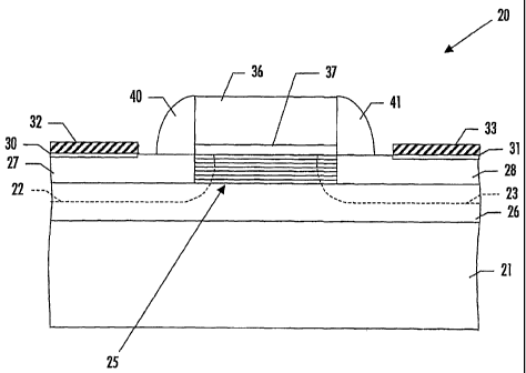
superlattice 25 material for a channel region in a MOSFET
device. A planar MOSFET 20 including the strained
superlattice 25 in accordance with the invention is now
first described with reference to FIG. 1. One skilled in
the art, however, will appreciate that the materials
identified herein could be used in many different types
of semiconductor devices, such as discrete devices and/or
integrated circuits. By way of example, another
application in which the strained superlattice 25 may be
CA 02612118 2007-12-13
WO 2007/011627 PCT/US2006/027119
used is in FINFETs, as further described in U.S.
Application Serial No. 11/426,969, which is assigned to
the present Assignee and is hereby incorporated herein in
its entirety by reference.
[0035] The illustrated MOSFET 20 includes a substrate
21, a stress layer 26 on the substrate, semiconductor
regions 27, 28 on the stress layer, and the strained
superlattice layer 25 is on the stress layer between the
semiconductor regions. More particularly, the stress
layer 26 may be a graded semiconductor layer, such as a
graded silicon germanium layer. Moreover, the
semiconductor regions 26, 27 may be silicon or silicon
germanium regions, for example. The semiconductor regions
26, 27 are illustratively implanted with a dopant to
provide source and drain regions 22, 23 of the MOSFET 20,
as will be appreciated by those skilled in the art.
[0036] Various superlattice structures that may be
used in the MOSFET 20 are discussed further below. In the
case of a silicon-oxygen superlattice, the lattice
spacing of the superlattice layer 25 would ordinarily be
smaller than that of a silicon germanium stress layer 26.
However, the stress layer 26 in this example induces a
tensile strain in the superlattice layer 25, which may be
used to provide further mobility enhancement in N-channel
FETs, for example. Alternatively, the compositions of the
superlattice layer 25 and stress layer 26 may be chosen
so that the superlattice would otherwise have a larger
lattice spacing than the stress layer. This would
advantageously induce compressive strain in the
superlattice layer 25 that may advantageously provide
11
CA 02612118 2007-12-13
WO 2007/011627 PCT/US2006/027119
further mobility enhancement of the superlattice in P-
channel FET devices, for example.
[0037] In the illustrated embodiment, the stress layer
is a graded semiconductor layer graded in a vertical
direction, and the strained superlattice 25 is vertically
stacked on the graded semiconductor layer. In an
alternative embodiment illustrated in FIG. 6, the MOSFET
20' further includes a substantially ungraded
semiconductor layer 42' positioned between the graded
semiconductor layer 26' and a strained superlattice layer
425'. That is, the substantially ungraded semiconductor
layer 42' has a substantially consistent composition of
semiconductor material (e.g., silicon germanium)
throughout from top to bottom and provides a buffer
between the stress layer 26' and the superlattice layer
425'. More particularly, the substantially ungraded
semiconductor layer 42' may have substantially the same
composition as the semiconductor material at the top of
the stress layer 42'. Further information on the use of
graded and ungraded layers for straining an overlying
semiconductor layer (e.g., silicon) may be found in U.S.
Patent Publication Nos. 2005/0211982 to Lei et al,
2005/0054175 to Bauer, 2005/0224800 to Lindert et al.,
and 2005/0051795 to Arena et al., all of which are hereby
incorporated herein in their entireties by reference.
[0038] Source/drain silicide layers 30, 31 and
source/drain contacts 32, 33 illustratively overlie the
source/drain regions 22, 23, as will be appreciated by
those skilled in the art. A gate 35 illustratively
includes a gate insulating layer 37 adjacent the channel
provided by the strained superlattice layer 25, and a
12
CA 02612118 2007-12-13
WO 2007/011627 PCT/US2006/027119
gate electrode layer 36 on the gate insulating layer.
Sidewall spacers 40, 41 are also provided in the
illustrated MOSFET 20.
[0039] It is also theorized that the semiconductor
device, such as the illustrated MOSFET 20, enjoys a
higher charge carrier mobility based upon the lower
conductivity effective mass than would otherwise be
present. In some embodiments, and as a result of the band
engineering, the superlattice 25 may further have a
substantially direct energy bandgap that may be
particularly advantageous for opto-electronic devices,
for example, such as those set forth in the co-pending
application entitled INTEGRATED CIRCUIT COMPRISING AN
ACTIVE OPTICAL DEVICE HAVING AN ENERGY BAND ENGINEERED
SUPERLATTICE, U.S. Patent Application Serial No.
10/936,903, which is assigned to the present Assignee and
is hereby incorporated herein in its entirety by
reference.
[0040] As will be appreciated by those skilled in the
art, the source/drain regions 22, 23 and gate 35 of the
MOSFET 20 may be considered as regions for causing the
transport of charge carriers through the strained
superlattice layer 25 in a parallel direction relative to
the layers of the stacked groups 45a-45n, as will be
discussed further below. That is, the channel of the
device is defined within the superlattice 25. Other such
regions are also contemplated by the present invention.
[0041] In certain embodiments, the superlattice 25 may
advantageously act as an interface for the gate
dielectric layer 37. For example, the channel region may
be defined in the lower portion of the superlattice 25
13
CA 02612118 2007-12-13
WO 2007/011627 PCT/US2006/027119
(although some of the channel may also be defined in the
semiconductor material below the superlattice), while the
upper portion thereof insulates the channel from the
dielectric layer 37. In still another embodiment, the
channel may be defined solely in the stress layer 26, and
the strained superlattice layer 25 may be included merely
as an insulation/interface layer.
[0042] Use of the superlattice 25 as a dielectric
interface layer may be particularly appropriate where
relatively high-K gate dielectric materials are used. The
superlattice 25 may advantageously provide reduced
scattering and, thus, enhanced mobility with respect to
prior art insulation layers (e.g., silicon oxides)
typically used for high-K dielectric interfaces.
Moreover, use of the superlattice 25 as an insulator for
applications with high-K dielectrics may result in
smaller overall thicknesses, and thus improved device
capacitance. This is because the superlattice 25 may be
formed in relatively small thicknesses yet still provide
desired insulating properties, as discussed further in
co-pending U.S. Application Serial No. 11/136,881, which
is assigned to the present Assignee and is hereby
incorporated herein in its entirety by reference.
[0043] Applicants have identified improved materials
or structures for the channel region of the MOSFET 20.
More specifically, the Applicants have identified
materials or structures having energy band structures for
which the appropriate conductivity effective masses for
electrons and/or holes are substantially less than the
corresponding values for silicon.
14
CA 02612118 2007-12-13
WO 2007/011627 PCT/US2006/027119
[0044] Referring now additionally to FIGS. 2 and 3,
the materials or structures are in the form of a
superlattice 25 whose structure is controlled at the
atomic or molecular level and may be formed using known
techniques of atomic or molecular layer deposition. The
superlattice 25 includes a plurality of layer groups 45a-
45n arranged in stacked relation, as perhaps best
understood with specific reference to the schematic
cross-sectional view of FIG. 2. Moreover, an intermediate
annealing process as described in co-pending U.S.
Application Serial No. 11/136,834, which is assigned to
the present Assignee and is hereby incorporated herein in
its entirety by reference, may also be used to
advantageously reduce defects and provide smother layer
surfaces during fabrication.
[0045] Each group of layers 45a-45n of the
superlattice 25 illustratively includes a plurality of
stacked base semiconductor monolayers 46 defining a
respective base semiconductor portion 46a-46n and an
energy band-modifying layer 50 thereon. The energy band-
modifying layers 50 are indicated by stippling in FIG. 2
for clarity of explanation.
[0046] The energy-band modifying layer 50
illustratively comprises one non-semiconductor monolayer
constrained within a crystal lattice of adjacent base
semiconductor portions. That is, opposing base
semiconductor monolayers 46 in adjacent groups of layers
45a-45n are chemically bound together. For example, in
the case of silicon monolayers 46, some of the silicon
atoms in the upper or top semiconductor monolayer of the
group of monolayers 46a will be covalently bonded with
CA 02612118 2007-12-13
WO 2007/011627 PCT/US2006/027119
silicon atoms in the lower or bottom monolayer of the
group 46b, as seen in FIG. 3. This allows the crystal
lattice to continue through the groups of layers despite
the presence of the non-semiconductor monolayer(s) (e.g.,
oxygen monolayer(s)). Of course, there will not be a
complete or pure covalent bond between the opposing
silicon layers 46 of adjacent groups 45a-45n as some of
the silicon atoms in each of these layers will be bonded
to non-semiconductor atoms (i.e., oxygen in the present
example), as will be appreciated by those skilled in the
art.
[0047] In other embodiments, more than one such
monolayer may be possible. It should be noted that
reference herein to a non-semiconductor or semiconductor
monolayer means that the material used for the monolayer
would be a non-semiconductor or semiconductor if formed
in bulk. That is, a single monolayer of a material, such
as semiconductor, may not necessarily exhibit the same
properties that it would if formed in bulk or in a
relatively thick layer, as will be appreciated by those
skilled in the art.
[0048] Applicants theorize without wishing to be bound
thereto that energy band-modifying layers 50 and adjacent
base semiconductor portions 46a-46n cause the
superlattice 25 to have a lower appropriate conductivity
effective mass for the charge carriers in the parallel
layer direction than would otherwise be present.
Considered another way, this parallel direction is
orthogonal to the stacking direction. The band modifying
layers 50 may also cause the superlattice 25 to have a
common energy band structure.
16
CA 02612118 2007-12-13
WO 2007/011627 PCT/US2006/027119
[0049] It is also theorized that the semiconductor
device, such as the illustrated MOSFET 20, enjoys a
higher charge carrier mobility based upon the lower
conductivity effective mass than would otherwise be
present. In some embodiments, and as a result of the band
engineering achieved by the present invention, the
superlattice 25 may further have a substantially direct
energy bandgap that may be particularly advantageous for
opto-electronic devices, for example, as described in
further detail below. Of course, all of the above-
described properties of the superlattice 25 need not be
utilized in every application. For example, in some
applications the superlattice 25 may only be used for its
dopant blocking/insulation properties or its enhanced
mobility, or it may be used for both in other
applications, as will be appreciated by those skilled in
the art.
[0050] In some embodiments, more than one non-
semiconductor monolayer may be present in the energy band
modifying layer 50. By way of example, the number of non-
semiconductor monolayers in the energy band-modifying
layer 50 may preferably be less than about five
monolayers to thereby provide the desired energy band-
modifying properties.
[0051] The superlattice 25 also illustratively
includes a cap layer 52 on an upper layer group 45n. The
cap layer 52 may comprise a plurality of base
semiconductor monolayers 46. The cap layer 52 may have
between 2 to 100 monolayers of the base semiconductor,
and, more preferably between 10 to 50 monolayers.
17
CA 02612118 2007-12-13
WO 2007/011627 PCT/US2006/027119
[0052] Each base semiconductor portion 46a-46n may
comprise a base semiconductor selected from the group
consisting of Group IV semiconductors, Group III-V
semiconductors, and Group II-VI semiconductors. Of
course, the term Group IV semiconductors also includes
Group IV-IV semiconductors as will be appreciated by
those skilled in the art. More particularly, the base
semiconductor may comprise at least one of silicon and
germanium, for example.
[0053] Each energy band-modifying layer 50 may
comprise a non-semiconductor selected from the group
consisting of oxygen, nitrogen, fluorine, and carbon-
oxygen, for example. The non-semiconductor is also
desirably thermally stable through deposition of a next
layer to thereby facilitate manufacturing. In other
embodiments, the non-semiconductor may be another
inorganic or organic element or compound that is
compatible with the given semiconductor processing as
will be appreciated by those skilled in the art.
[0054] It should be noted that the term monolayer is
meant to include a single atomic layer and also a single
molecular layer. It is also noted that the energy band-
modifying layer 50 provided by a single monolayer is also
meant to include a monolayer wherein not all of the
possible sites are occupied, as noted above. For example,
with particular reference to the atomic diagram of FIG.
3, a 4/1 repeating structure is illustrated for silicon
as the base semiconductor material, and oxygen as the
energy band-modifying material. Only half of the possible
sites for oxygen are occupied.
18
CA 02612118 2007-12-13
WO 2007/011627 PCT/US2006/027119
[0055] In other embodiments and/or with different
materials this one half occupation would not necessarily
be the case, as will be appreciated by those skilled in
the art. Indeed it can be seen even in this schematic
diagram, that individual atoms of oxygen in a given
monolayer are not precisely aligned along a flat plane as
will also be appreciated by those of skill in the art of
atomic deposition. By way of example, a preferred
occupation range is from about one-eighth to one-half of
the possible oxygen sites being full, although other
numbers may be used in certain embodiments.
[0056] Silicon and oxygen are currently widely used in
conventional semiconductor processing, and, hence,
manufacturers will be readily able to use these materials
as described herein. Atomic or monolayer deposition is
also now widely used. Accordingly, semiconductor devices
incorporating the superlattice 25 may be readily adopted
and implemented as will be appreciated by those skilled
in the art.
[0057] It is theorized without Applicants wishing to
be bound thereto that for a superlattice, such as the
Si/O superlattice, for example, that the number of
silicon monolayers should desirably be seven or less so
that the energy band of the superlattice is common or
relatively uniform throughout to achieve the desired
advantages. Of course, more than seven silicon layers may
be used in some embodiments. The 4/1 repeating structure
shown in FIGS. 2 and 3, for Si/0 has been modeled to
indicate an enhanced mobility for electrons and holes in
the X direction. For example, the calculated conductivity
effective mass for electrons (isotropic for bulk silicon)
19
CA 02612118 2007-12-13
WO 2007/011627 PCT/US2006/027119
is 0.26 and for the 4/1 SiO superlattice in the X
direction it is 0.12 resulting in a ratio of 0.46.
Similarly, the calculation for holes yields values of
0.36 for bulk silicon and 0.16 for the 4/1 Si/O
superlattice resulting in a ratio of 0.44.
[0058] While such a directionally preferential feature
may be desired in certain semiconductor devices, other
devices may benefit from a more uniform increase in
mobility in any direction parallel to the groups of
layers. It may also be beneficial to have an increased
mobility for both electrons or holes, or just one of
these types of charge carriers as will be appreciated by
those skilled in the art.
[0059] The lower conductivity effective mass for the
4/1 Si/0 embodiment of the superlattice 25 may be less
than two-thirds the conductivity effective mass than
would otherwise occur, and this applies for both
electrons and holes. Of course, the superlattice 25 may
further comprise at least one type of conductivity dopant
therein as will also be appreciated by those skilled in
the art. It may be especially appropriate to dope at
least a portion of the superlattice 25 if the
superlattice is to provide some or all of the channel.
However, the superlattice 25 or portions thereof may also
remain substantially undoped in some embodiments, as
described further in U.S. Application Serial No.
11/136,757, which is assigned to the present Assignee and
is hereby incorporated herein in its entirety by
reference.
[0060] Referring now additionally to FIG. 4, another
embodiment of a superlattice 25' in accordance with the
CA 02612118 2007-12-13
WO 2007/011627 PCT/US2006/027119
invention having different properties is now described.
In this embodiment, a repeating pattern of 3/1/5/1 is
illustrated. More particularly, the lowest base
semiconductor portion 46a' has three monolayers, and the
second lowest base semiconductor portion 46b' has five
monolayers. This pattern repeats throughout the
superlattice 25'. The energy band-modifying layers 50'
may each include a single monolayer. For such a
superlattice 25' including Si/O, the enhancement of
charge carrier mobility is independent of orientation in
the plane of the layers. Those other elements of FIG. 4
not specifically mentioned are similar to those discussed
above with reference to FIG. 2 and need no further
discussion herein.
[0061] In some device embodiments, all of the base
semiconductor portions of a superlattice may be a same
number of monolayers thick. In other embodiments, at
least some of the base semiconductor portions may be a
different number of monolayers thick. In still other
embodiments, all of the base semiconductor portions may
be a different number of monolayers thick.
[0062] In FIGS. 5A-5C band structures calculated using
Density Functional Theory (DFT) are presented. It is well
known in the art that DFT underestimates the absolute
value of the bandgap. Hence all bands above the gap may
be shifted by an appropriate "scissors correction."
However, the shape of the band is known to be much more
reliable. The vertical energy axes should be interpreted
in this light.
[0063] FIG. 5A shows the calculated band structure
from the gamma point (G) for both bulk silicon
21
CA 02612118 2007-12-13
WO 2007/011627 PCT/US2006/027119
(represented by continuous lines) and for the 4/1 Si/O
superlattice 25 as shown in FIGS. 1-3 (represented by
dotted lines). The directions refer to the unit cell of
the 4/1 Si/O structure and not to the conventional unit
cell of Si, although the (001) direction in the figure
does correspond to the (001) direction of the
conventional unit cell of Si, and, hence, shows the
expected location of the Si conduction band minimum. The
(100) and (010) directions in the figure correspond to
the (110) and (-110) directions of the conventional Si
unit cell. Those skilled in the art will appreciate that
the bands of Si on the figure are folded to represent
them on the appropriate reciprocal lattice directions for
the 4/1 Si/O structure.
[0064] It can be seen that the conduction band minimum
for the 4/1 Si/O structure is located at the gamma point
in contrast to bulk silicon (Si), whereas the valence
band minimum occurs at the edge of the Brillouin zone in
the (001) direction which we refer to as the Z point. One
may also note the greater curvature of the conduction
band minimum for the 4/1 Si/O structure compared to the
curvature of the conduction band minimum for Si owing to
the band splitting due to the perturbation introduced by
the additional oxygen layer.
[0065] FIG. 5B shows the calculated band structure
from the Z point for both bulk silicon (continuous lines)
and for the 4/1 Si/O superlattice 25 (dotted lines). This
figure illustrates the enhanced curvature of the valence
band in the (100) direction.
[0066] FIG. 5C shows the calculated band structure
from the both the gamma and Z point for both bulk silicon
22
CA 02612118 2007-12-13
WO 2007/011627 PCT/US2006/027119
(continuous lines) and for the 5/1/3/1 Si/O structure of
the superlattice 25' of FIG. 4 (dotted lines). Due to the
symmetry of the 5/1/3/1 Si/O structure, the calculated
band structures in the (100) and (010) directions are
equivalent. Thus the conductivity effective mass and
mobility are expected to be isotropic in the plane
parallel to the layers, i.e. perpendicular to the (001)
stacking direction. Note that in the 5/1/3/1 Si/O example
the conduction band minimum and the valence band maximum
are both at or close to the Z point.
[0067] Although increased curvature is an indication
of reduced effective mass, the appropriate comparison and
discrimination may be made via the conductivity
reciprocal effective mass tensor calculation. This leads
Applicants to further theorize that the 5/1/3/1
superlattice 25' should be substantially direct bandgap.
As will be understood by those skilled in the art, the
appropriate matrix element for optical transition is
another indicator of the distinction between direct and
indirect bandgap behavior.
[0068] Turning additionally to FIGS. 7-9, additional
embodiments of MOSFETs 120, 220, and 320 each including a
strained superlattice layer are now described. In the
illustrated embodiments, the various layers and regions
that are similar to those discussed above with reference
to FIG. 1 are represented by increments of one hundred
(e.g., the substrates 121, 221, and 321 shown in FIGS. 7-
9, respectively, are similar to the substrate 21).
[0069] In the MOSFET 120, the stress layer is provided
by a plurality of spaced apart strain inducing pillars
144 arranged in side-by-side relation on the backside
23
CA 02612118 2007-12-13
WO 2007/011627 PCT/US2006/027119
(i.e., bottom) of the substrate 121. By way of example,
if compressive strain is desired then the pillars 144 may
include plasma enhanced chemical vapor deposition (PECVD)
silicon nitride (SiN), metal, or other materials which
become compressed upon or after being deposited in
trenches etched in the backside of the substrate 121.
Moreover, if tensile strain is desired then the pillars
may include a thermally formed SiN material or low
pressure chemical vapor deposition (LPCVD) SiN material,
for example. Of course, other suitable materials known to
those skilled in the art may also be used. Further
details on a backside strain-inducing pillar arrangement
may be found in U.S. Patent Publication No. 2005/0263753
to Pelella et al., which is hereby incorporated herein in
its entirety by reference.
[0070] Moreover, an insulating layer 143 (shown with
stippling for clarity of illustration), such as an Si02
layer, may also be positioned between the stress layer
125 and the strained superlattice layer to provide a
semiconductor-on-insulator embodiment, as shown, although
the insulating layer need not be used in all embodiments.
Further details on forming a superlattice structure as
set forth above on a semiconductor-on-insulator substrate
are provided in co-pending U.S. Application Serial No.
11/381,835, which is assigned to the present Assignee and
is hereby incorporated herein in its entirety by
reference. Of course, semiconductor-on-insulator
implementations may be used in other embodiments
discussed herein as well.
[0071] Referring to FIG. 8, in the MOSFET 220 the
regions 327, 328 define a pair of spaced apart stress
24
CA 02612118 2007-12-13
WO 2007/011627 PCT/US2006/027119
regions for inducing strain in the superlattice layer 125
positioned therebetween. More particularly, one or both
of the stress regions may include a material that induces
a desired strain on the superlattice layer 225. Using the
above-noted example, for a silicon-oxygen superlattice
layer 225 one or both of the regions 327, 328 may include
silicon germanium. Yet, whereas in the MOSFET 20 the
silicon germanium induced a tensile strain when
positioned below the superlattice layer 25, when
positioned on one or both sides of the superlattice layer
225 the silicon germanium has the opposite effect and
compresses the superlattice.
[0072] Thus, in the illustrated embodiment silicon
germanium in the stress regions 227, 228 would be
advantageous for P-channel implementations because it
induces compressive strain. Alternatively, a tensile
strain could advantageously be induced in the
superlattice layer 225 for N-channel devices by properly
selecting the composition of the superlattice and the
stress regions 227, 228, as discussed above. It should be
noted that in some embodiments the spaced apart stress
regions 227, 228 need not include the same materials.
That is, strain may be induced as one stress region
"pushes" or "pulls" against the other which serves as an
anchor.
[0073] In the above-described embodiment, the pair of
stress regions 227, 228 are doped to provide the source
and drain regions 222, 223. Moreover, the stress regions
227, 228 illustratively include canted surfaces or facets
245, 246 adjacent opposing portions of the strained
superlattice. The canted surfaces 245, 246 may result
CA 02612118 2007-12-13
WO 2007/011627 PCT/US2006/027119
from the etching process used to pattern the superlattice
225 so that the stress inducing material can be deposited
adjacent thereto. However, the surfaces 245, 246 need not
be canted in all embodiments. Further details on making
strained channel devices with strain-inducing source and
drain regions are disclosed in U.S. Patent No. 6,495,402
to Yu et al. and U.S. Patent Publication No. 2005/0142768
to Lindert et al., both of which are hereby incorporated
herein in their entireties by reference.
[0074] Referring to FIG. 9, the MOSFET 320
illustratively includes a stress layer 347 above the
strained superlattice layer 325. By way of example, the
stress layer may be a SiN layer deposited over the
source, drain, and gate regions of the MOSFET 320 that
induces a strain in the underlying semiconductor
material, including the superlattice layer 325. As noted
above, a tensile or compressive nitride material may be
used depending upon the type of strain desired in the
superlattice layer 325. Of course, other suitable
materials may also be used for the stress layer 347, and
multiple stress layers may be used in some embodiments.
Moreover, in certain embodiments the superlattice layer
325 may "memorize" the strain induced from the overlying
stress layer 347, and the stress layer may thereafter be
removed, as will be appreciated by those skilled in the
art. Further details on creating strain in semiconductor
regions using overlying stress layers may be found in
U.S. Patent Publication Nos. 2005/0145894 to Chau et al.
and 2005/0247926 to Sun et al., both of which are hereby
incorporated herein in their entireties by reference.
26
CA 02612118 2007-12-13
WO 2007/011627 PCT/US2006/027119
[0075] A first method aspect in accordance with the
invention for making a semiconductor device, such as the
MOSFET 20, is now described. The method includes forming
a stress layer 26, and forming a strained superlattice
layer 25 above the stress layer. Another method aspect is
for making a semiconductor device, such as the MOSFET
220, which includes forming a superlattice layer 225, and
forming at least one pair of spaced apart stress regions
227, 228 on opposing sides of the superlattice layer to
induce a strain therein. Still another method aspect is
for making a semiconductor device, such as the MOSFET
320, which includes forming a superlattice layer 325, and
forming a stress layer 347 above the strained
superlattice layer to induce a strain therein. Various
other method steps and aspects will be appreciated by
those skilled in the art from the foregoing description
and therefore require no further discussion herein.
[0076] It should be noted that in the above-described
embodiments, the strained layer need not always be a
superlattice 25. Rather, the strained layer may simply
include a plurality of base semiconductor portions 46a-
46n, and one or more non-semiconductor monolayers 50
constrained within a crystal lattice of adjacent base
semiconductor portions (i.e., the adjacent base
semiconductor portions are chemically bound together, as
described above). In this embodiment, the base
semiconductor portions 46a-46n need not include a
plurality of semiconductor monolayers, i.e., each
semiconductor portion could include a single layer or a
plurality of monolayers, for example.
27
CA 02612118 2007-12-13
WO 2007/011627 PCT/US2006/027119
[0077] A MOSFET 80 illustratively including a non-
semiconductor monolayer 81 is schematically shown in FIG.
wherein the semiconductor monolayers are in the
portions 82a, 82b respectively below and above the non-
semiconductor monolayer. The gate dielectric 83 is
illustratively above the channel 85, and the gate
electrode 84 is above the gate dielectric. The region
between the lower portion of the gate dielectric 83 and
the upper portion of the channel 85 define an interface
86. The source and drain (not shown) would be positioned
laterally adjacent the channel 85, as will be appreciated
by those skilled in the art.
[0078] The depth of the monolayer of non-semiconductor
material 81 from the interface 86 may be selected based
upon the MOSFET design, as will be appreciated by those
skilled in the art. For example, a depth of about 4-100
monolayers, and more preferably a depth of about 4-30
monolayers, may be selected for a typical MOSFET 86 for
an oxygen layer in a silicon channel. The at least one
monolayer of non-semiconductor material may include one
or more monolayers that are not fully populated in all of
the available sites as described above.
[0079] As discussed above, the non-semiconductor may
be selected from the group consisting of oxygen,
nitrogen, fluorine, and carbon-oxygen, for example. The
at least one monolayer of non-semiconductor material 81
may be deposited using atomic layer deposition
techniques, for example, as also described above and as
will be appreciated by those skilled in the art. Other
deposition and/or implantation methods may also be used
to form the channel 85 to include the at least one non-
28
CA 02612118 2007-12-13
WO 2007/011627 PCT/US2006/027119
semiconductor material layer 81 within the crystal
lattice of adjacent semiconductor layers 82a, 82b.
[0080] A simulated plot 90 of density at the interface
versus depth of an oxygen layer in Angstroms is shown in
FIG. 11. As will be appreciated by those skilled in the
art, in embodiments such as the illustrated MOSFET 80,
repeating groups of the superlattice need not be used,
yet the at least one non-semiconductor monolayer 81 may
still provide enhancement to mobility. In addition,
Applicants also theorize without wishing to be bound
thereto that these embodiments will also have lower
tunneling gate leakage as a result of the reduced
magnitude of the wave functions at the interface 86. It
is also theorized that further desirable features of
these embodiments include increased energy separation
between sub-bands, and the spatial separation of sub-
bands, thereby reducing sub-band scattering.
[0081] Of course in other embodiments, the at least
one monolayer 81 may also be used in combination with an
underlying superlattice as will also be appreciated by
those skilled in the art. Further, many modifications and
other embodiments of the invention will come to the mind
of one skilled in the art having the benefit of the
teachings presented in the foregoing descriptions and the
associated drawings. Therefore, it is understood that the
invention is not to be limited to the specific
embodiments disclosed, and that modifications and
embodiments are intended.
29