Some of the information on this Web page has been provided by external sources. The Government of Canada is not responsible for the accuracy, reliability or currency of the information supplied by external sources. Users wishing to rely upon this information should consult directly with the source of the information. Content provided by external sources is not subject to official languages, privacy and accessibility requirements.
Any discrepancies in the text and image of the Claims and Abstract are due to differing posting times. Text of the Claims and Abstract are posted:
| (12) Patent: | (11) CA 2612194 |
|---|---|
| (54) English Title: | IMAGE SENSOR ARCHITECTURE EMPLOYING ONE OR MORE FLOATING GATE DEVICES |
| (54) French Title: | ARCHITECTURE DE CAPTEUR D'IMAGE UTILISANT UN OU PLUSIEURS DISPOSITIFS DE PORTE FLOTTANTE |
| Status: | Expired and beyond the Period of Reversal |
| (51) International Patent Classification (IPC): |
|
|---|---|
| (72) Inventors : |
|
| (73) Owners : |
|
| (71) Applicants : |
|
| (74) Agent: | GOWLING WLG (CANADA) LLP |
| (74) Associate agent: | |
| (45) Issued: | 2014-07-08 |
| (86) PCT Filing Date: | 2006-05-23 |
| (87) Open to Public Inspection: | 2007-01-04 |
| Examination requested: | 2011-02-07 |
| Availability of licence: | N/A |
| Dedicated to the Public: | N/A |
| (25) Language of filing: | English |
| Patent Cooperation Treaty (PCT): | Yes |
|---|---|
| (86) PCT Filing Number: | PCT/US2006/019724 |
| (87) International Publication Number: | US2006019724 |
| (85) National Entry: | 2007-12-14 |
| (30) Application Priority Data: | ||||||
|---|---|---|---|---|---|---|
|
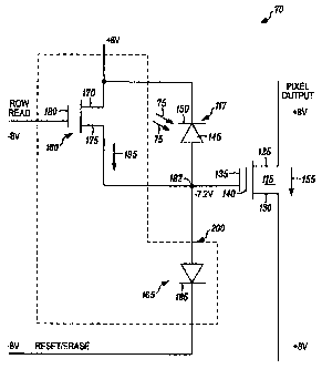
A circuit for use in an image sensor as well as an image sensing system using
the circuit are set forth. The circuit comprises a floating gate semiconductor
device having a floating gate, a control gate, a drain and a source. The
circuit also employs a photosensitive semiconductor device that is positioned
for exposure to electromagnetic radiation from an image. A pixel control
circuit is connected to these components to direct the floating gate
semiconductor device and the photosensitive semiconductor device to a
plurality of controlled modes. The controlled modes may include an erase mode
and an exposure mode. In the erase mode, at least a portion of an electric
charge is removed from the floating gate to place the floating gate
semiconductor device in an initialized state. In the exposure mode, the
floating gate is charged at least partially in response to a voltage at a
terminal of the photosensitive semiconductor device. The voltage at the
terminal of the photosensitive semiconductor device corresponds to exposure of
the photosensitive semiconductor device to the electromagnetic radiation from
the image. The pixel control circuit may also direct the floating gate
semiconductor device and the photosensitive semiconductor device to further
modes including a read mode and a data retention mode. In the read mode,
current flow between the source and drain of the floating gate semiconductor
device is detected as an indicator of the charge on the floating gate. In the
data retention mode, the charge on the floating gate of the floating gate
semiconductor device that was acquired during the exposure mode is maintained
notwithstanding further exposure of the photosensitive semiconductor device to
the electromagnetic radiation from the image. The circuit, and one or more
peripheral support circuits, may be implemented in a monolithic substrate
using, for example, conventional CMOS manufacturing processes.
La présente invention concerne un circuit destiné à être utilisé dans un capteur d'image ainsi qu'un système de saisie d'image comprenant ledit circuit. Le circuit comprend un dispositif semiconducteur à porte flottante comportant une porte flottante, une porte de commande, un drain et une source. Le circuit utilise également un dispositif semiconducteur photosensible qui est positionné pour être exposé au rayonnement électromagnétique d'une image. Un circuit de commande des pixels est couplé à ces constituants pour commander le dispositif semiconducteur à porte flottante et le dispositif semiconducteur photosensible dans de multiples modes commandés. Les modes commandés peuvent comprendre un mode d'effacement et un mode d'exposition. Dans le mode d'effacement, au moins une partie d'une charge électrique est éliminée de la porte flottante pour placer le dispositif semiconducteur à porte flottante dans un état initialisé. Dans le mode d'exposition, la porte flottante est chargée au moins partiellement en réponse à une tension appliquée à une borne du dispositif semiconducteur photosensible. La tension à la borne du dispositif semiconducteur photosensible correspond à l'exposition du dispositif semiconducteur photosensible au rayonnement électromagnétique de l'image. Le circuit de commande des pixels peut également commander le dispositif semiconducteur à porte flottante et le dispositif semiconducteur photosensible dans d'autres modes comprenant un mode de lecture et un mode de rétention des données. Dans le mode de lecture, le flux de courant entre la source et le drain du dispositif semiconducteur à porte flottante est détecté en tant qu'indicateur de la charge appliquée sur la porte flottante. Dans le mode de rétention des données, la charge sur la porte flottante du dispositif semiconducteur à porte flottante qui a été acquise pendant le mode d'exposition est maintenue malgré toute autre exposition du dispositif semiconducteur photosensible au rayonnement électromagnétique de l'image. Le circuit ainsi qu'au moins un circuit de soutien périphérique peuvent être mis en oeuvre dans un substrat monolithique au moyen par exemple de processus de fabrication CMOS classiques.
Note: Claims are shown in the official language in which they were submitted.
Note: Descriptions are shown in the official language in which they were submitted.
2024-08-01:As part of the Next Generation Patents (NGP) transition, the Canadian Patents Database (CPD) now contains a more detailed Event History, which replicates the Event Log of our new back-office solution.
Please note that "Inactive:" events refers to events no longer in use in our new back-office solution.
For a clearer understanding of the status of the application/patent presented on this page, the site Disclaimer , as well as the definitions for Patent , Event History , Maintenance Fee and Payment History should be consulted.
| Description | Date |
|---|---|
| Inactive: IPC expired | 2023-01-01 |
| Inactive: IPC expired | 2023-01-01 |
| Time Limit for Reversal Expired | 2017-05-23 |
| Letter Sent | 2016-05-24 |
| Grant by Issuance | 2014-07-08 |
| Inactive: Cover page published | 2014-07-07 |
| Pre-grant | 2014-03-24 |
| Inactive: Final fee received | 2014-03-24 |
| Notice of Allowance is Issued | 2014-03-13 |
| Letter Sent | 2014-03-13 |
| Notice of Allowance is Issued | 2014-03-13 |
| Inactive: Received pages at allowance | 2014-02-20 |
| Inactive: Correction to amendment | 2013-12-10 |
| Inactive: Approved for allowance (AFA) | 2013-11-22 |
| Inactive: Q2 passed | 2013-11-22 |
| Amendment Received - Voluntary Amendment | 2013-06-21 |
| Inactive: S.30(2) Rules - Examiner requisition | 2013-02-07 |
| Letter Sent | 2011-12-28 |
| Inactive: Multiple transfers | 2011-12-14 |
| Inactive: IPC deactivated | 2011-07-29 |
| Letter Sent | 2011-03-21 |
| Inactive: IPC assigned | 2011-03-18 |
| Inactive: IPC removed | 2011-03-18 |
| Inactive: First IPC assigned | 2011-03-18 |
| Inactive: IPC assigned | 2011-03-18 |
| Request for Examination Received | 2011-02-07 |
| Request for Examination Requirements Determined Compliant | 2011-02-07 |
| All Requirements for Examination Determined Compliant | 2011-02-07 |
| Inactive: IPC expired | 2011-01-01 |
| Inactive: Cover page published | 2008-03-17 |
| Inactive: Notice - National entry - No RFE | 2008-03-14 |
| Inactive: First IPC assigned | 2008-01-12 |
| Application Received - PCT | 2008-01-11 |
| National Entry Requirements Determined Compliant | 2007-12-14 |
| Application Published (Open to Public Inspection) | 2007-01-04 |
There is no abandonment history.
The last payment was received on 2014-04-22
Note : If the full payment has not been received on or before the date indicated, a further fee may be required which may be one of the following
Patent fees are adjusted on the 1st of January every year. The amounts above are the current amounts if received by December 31 of the current year.
Please refer to the CIPO
Patent Fees
web page to see all current fee amounts.
| Fee Type | Anniversary Year | Due Date | Paid Date |
|---|---|---|---|
| Basic national fee - standard | 2007-12-14 | ||
| MF (application, 2nd anniv.) - standard | 02 | 2008-05-23 | 2008-04-07 |
| MF (application, 3rd anniv.) - standard | 03 | 2009-05-25 | 2009-03-30 |
| MF (application, 4th anniv.) - standard | 04 | 2010-05-25 | 2010-04-22 |
| Request for examination - standard | 2011-02-07 | ||
| MF (application, 5th anniv.) - standard | 05 | 2011-05-24 | 2011-04-19 |
| Registration of a document | 2011-12-14 | ||
| MF (application, 6th anniv.) - standard | 06 | 2012-05-23 | 2012-04-13 |
| MF (application, 7th anniv.) - standard | 07 | 2013-05-23 | 2013-04-15 |
| Final fee - standard | 2014-03-24 | ||
| MF (application, 8th anniv.) - standard | 08 | 2014-05-23 | 2014-04-22 |
| MF (patent, 9th anniv.) - standard | 2015-05-25 | 2015-05-19 |
Note: Records showing the ownership history in alphabetical order.
| Current Owners on Record |
|---|
| MOTOROLA MOBILITY, INC. |
| Past Owners on Record |
|---|
| CARL L. SHURBOFF |
| FAN HE |

