Une partie des informations de ce site Web a été fournie par des sources externes. Le gouvernement du Canada n'assume aucune responsabilité concernant la précision, l'actualité ou la fiabilité des informations fournies par les sources externes. Les utilisateurs qui désirent employer cette information devraient consulter directement la source des informations. Le contenu fourni par les sources externes n'est pas assujetti aux exigences sur les langues officielles, la protection des renseignements personnels et l'accessibilité.
L'apparition de différences dans le texte et l'image des Revendications et de l'Abrégé dépend du moment auquel le document est publié. Les textes des Revendications et de l'Abrégé sont affichés :
| (12) Brevet: | (11) CA 2612194 |
|---|---|
| (54) Titre français: | ARCHITECTURE DE CAPTEUR D'IMAGE UTILISANT UN OU PLUSIEURS DISPOSITIFS DE PORTE FLOTTANTE |
| (54) Titre anglais: | IMAGE SENSOR ARCHITECTURE EMPLOYING ONE OR MORE FLOATING GATE DEVICES |
| Statut: | Périmé et au-delà du délai pour l’annulation |
| (51) Classification internationale des brevets (CIB): |
|
|---|---|
| (72) Inventeurs : |
|
| (73) Titulaires : |
|
| (71) Demandeurs : |
|
| (74) Agent: | GOWLING WLG (CANADA) LLP |
| (74) Co-agent: | |
| (45) Délivré: | 2014-07-08 |
| (86) Date de dépôt PCT: | 2006-05-23 |
| (87) Mise à la disponibilité du public: | 2007-01-04 |
| Requête d'examen: | 2011-02-07 |
| Licence disponible: | S.O. |
| Cédé au domaine public: | S.O. |
| (25) Langue des documents déposés: | Anglais |
| Traité de coopération en matière de brevets (PCT): | Oui |
|---|---|
| (86) Numéro de la demande PCT: | PCT/US2006/019724 |
| (87) Numéro de publication internationale PCT: | WO 2007001688 |
| (85) Entrée nationale: | 2007-12-14 |
| (30) Données de priorité de la demande: | ||||||
|---|---|---|---|---|---|---|
|
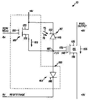
La présente invention concerne un circuit destiné à être utilisé dans un capteur d'image ainsi qu'un système de saisie d'image comprenant ledit circuit. Le circuit comprend un dispositif semiconducteur à porte flottante comportant une porte flottante, une porte de commande, un drain et une source. Le circuit utilise également un dispositif semiconducteur photosensible qui est positionné pour être exposé au rayonnement électromagnétique d'une image. Un circuit de commande des pixels est couplé à ces constituants pour commander le dispositif semiconducteur à porte flottante et le dispositif semiconducteur photosensible dans de multiples modes commandés. Les modes commandés peuvent comprendre un mode d'effacement et un mode d'exposition. Dans le mode d'effacement, au moins une partie d'une charge électrique est éliminée de la porte flottante pour placer le dispositif semiconducteur à porte flottante dans un état initialisé. Dans le mode d'exposition, la porte flottante est chargée au moins partiellement en réponse à une tension appliquée à une borne du dispositif semiconducteur photosensible. La tension à la borne du dispositif semiconducteur photosensible correspond à l'exposition du dispositif semiconducteur photosensible au rayonnement électromagnétique de l'image. Le circuit de commande des pixels peut également commander le dispositif semiconducteur à porte flottante et le dispositif semiconducteur photosensible dans d'autres modes comprenant un mode de lecture et un mode de rétention des données. Dans le mode de lecture, le flux de courant entre la source et le drain du dispositif semiconducteur à porte flottante est détecté en tant qu'indicateur de la charge appliquée sur la porte flottante. Dans le mode de rétention des données, la charge sur la porte flottante du dispositif semiconducteur à porte flottante qui a été acquise pendant le mode d'exposition est maintenue malgré toute autre exposition du dispositif semiconducteur photosensible au rayonnement électromagnétique de l'image. Le circuit ainsi qu'au moins un circuit de soutien périphérique peuvent être mis en oeuvre dans un substrat monolithique au moyen par exemple de processus de fabrication CMOS classiques.
A circuit for use in an image sensor as well as an image sensing system using
the circuit are set forth. The circuit comprises a floating gate semiconductor
device having a floating gate, a control gate, a drain and a source. The
circuit also employs a photosensitive semiconductor device that is positioned
for exposure to electromagnetic radiation from an image. A pixel control
circuit is connected to these components to direct the floating gate
semiconductor device and the photosensitive semiconductor device to a
plurality of controlled modes. The controlled modes may include an erase mode
and an exposure mode. In the erase mode, at least a portion of an electric
charge is removed from the floating gate to place the floating gate
semiconductor device in an initialized state. In the exposure mode, the
floating gate is charged at least partially in response to a voltage at a
terminal of the photosensitive semiconductor device. The voltage at the
terminal of the photosensitive semiconductor device corresponds to exposure of
the photosensitive semiconductor device to the electromagnetic radiation from
the image. The pixel control circuit may also direct the floating gate
semiconductor device and the photosensitive semiconductor device to further
modes including a read mode and a data retention mode. In the read mode,
current flow between the source and drain of the floating gate semiconductor
device is detected as an indicator of the charge on the floating gate. In the
data retention mode, the charge on the floating gate of the floating gate
semiconductor device that was acquired during the exposure mode is maintained
notwithstanding further exposure of the photosensitive semiconductor device to
the electromagnetic radiation from the image. The circuit, and one or more
peripheral support circuits, may be implemented in a monolithic substrate
using, for example, conventional CMOS manufacturing processes.
Note : Les revendications sont présentées dans la langue officielle dans laquelle elles ont été soumises.
Note : Les descriptions sont présentées dans la langue officielle dans laquelle elles ont été soumises.
2024-08-01 : Dans le cadre de la transition vers les Brevets de nouvelle génération (BNG), la base de données sur les brevets canadiens (BDBC) contient désormais un Historique d'événement plus détaillé, qui reproduit le Journal des événements de notre nouvelle solution interne.
Veuillez noter que les événements débutant par « Inactive : » se réfèrent à des événements qui ne sont plus utilisés dans notre nouvelle solution interne.
Pour une meilleure compréhension de l'état de la demande ou brevet qui figure sur cette page, la rubrique Mise en garde , et les descriptions de Brevet , Historique d'événement , Taxes périodiques et Historique des paiements devraient être consultées.
| Description | Date |
|---|---|
| Inactive : CIB expirée | 2023-01-01 |
| Inactive : CIB expirée | 2023-01-01 |
| Le délai pour l'annulation est expiré | 2017-05-23 |
| Lettre envoyée | 2016-05-24 |
| Accordé par délivrance | 2014-07-08 |
| Inactive : Page couverture publiée | 2014-07-07 |
| Préoctroi | 2014-03-24 |
| Inactive : Taxe finale reçue | 2014-03-24 |
| Un avis d'acceptation est envoyé | 2014-03-13 |
| Lettre envoyée | 2014-03-13 |
| Un avis d'acceptation est envoyé | 2014-03-13 |
| Inactive : Pages reçues à l'acceptation | 2014-02-20 |
| Inactive : Correction à la modification | 2013-12-10 |
| Inactive : Approuvée aux fins d'acceptation (AFA) | 2013-11-22 |
| Inactive : Q2 réussi | 2013-11-22 |
| Modification reçue - modification volontaire | 2013-06-21 |
| Inactive : Dem. de l'examinateur par.30(2) Règles | 2013-02-07 |
| Lettre envoyée | 2011-12-28 |
| Inactive : Transferts multiples | 2011-12-14 |
| Inactive : CIB désactivée | 2011-07-29 |
| Lettre envoyée | 2011-03-21 |
| Inactive : CIB attribuée | 2011-03-18 |
| Inactive : CIB enlevée | 2011-03-18 |
| Inactive : CIB en 1re position | 2011-03-18 |
| Inactive : CIB attribuée | 2011-03-18 |
| Requête d'examen reçue | 2011-02-07 |
| Exigences pour une requête d'examen - jugée conforme | 2011-02-07 |
| Toutes les exigences pour l'examen - jugée conforme | 2011-02-07 |
| Inactive : CIB expirée | 2011-01-01 |
| Inactive : Page couverture publiée | 2008-03-17 |
| Inactive : Notice - Entrée phase nat. - Pas de RE | 2008-03-14 |
| Inactive : CIB en 1re position | 2008-01-12 |
| Demande reçue - PCT | 2008-01-11 |
| Exigences pour l'entrée dans la phase nationale - jugée conforme | 2007-12-14 |
| Demande publiée (accessible au public) | 2007-01-04 |
Il n'y a pas d'historique d'abandonnement
Le dernier paiement a été reçu le 2014-04-22
Avis : Si le paiement en totalité n'a pas été reçu au plus tard à la date indiquée, une taxe supplémentaire peut être imposée, soit une des taxes suivantes :
Veuillez vous référer à la page web des taxes sur les brevets de l'OPIC pour voir tous les montants actuels des taxes.
| Type de taxes | Anniversaire | Échéance | Date payée |
|---|---|---|---|
| Taxe nationale de base - générale | 2007-12-14 | ||
| TM (demande, 2e anniv.) - générale | 02 | 2008-05-23 | 2008-04-07 |
| TM (demande, 3e anniv.) - générale | 03 | 2009-05-25 | 2009-03-30 |
| TM (demande, 4e anniv.) - générale | 04 | 2010-05-25 | 2010-04-22 |
| Requête d'examen - générale | 2011-02-07 | ||
| TM (demande, 5e anniv.) - générale | 05 | 2011-05-24 | 2011-04-19 |
| Enregistrement d'un document | 2011-12-14 | ||
| TM (demande, 6e anniv.) - générale | 06 | 2012-05-23 | 2012-04-13 |
| TM (demande, 7e anniv.) - générale | 07 | 2013-05-23 | 2013-04-15 |
| Taxe finale - générale | 2014-03-24 | ||
| TM (demande, 8e anniv.) - générale | 08 | 2014-05-23 | 2014-04-22 |
| TM (brevet, 9e anniv.) - générale | 2015-05-25 | 2015-05-19 |
Les titulaires actuels et antérieures au dossier sont affichés en ordre alphabétique.
| Titulaires actuels au dossier |
|---|
| MOTOROLA MOBILITY, INC. |
| Titulaires antérieures au dossier |
|---|
| CARL L. SHURBOFF |
| FAN HE |

