Note: Descriptions are shown in the official language in which they were submitted.
CA 02612978 2012-02-24
, .
SYNCHRONOUS ONE-BIT INTERFACE PROTOCOL OR DATA STRUCTURE
BACKGROUND
[0001] The present invention relates to data structures which include
first data (which,
e.g., may be referred to as message or payload data) that is coded and decoded
using a clock
period. According to embodiments of the invention, such a data structure also
includes
second data from which can be extracted the clock period used to code the
first data in the
data structure and with which the first data in the data structure can be
decoded. Such data
structures may be used in various data transfer and data communication
applications, e.g., to
transfer data between a computer terminal and a user device in connection with
authentication of the user.
[0002] The data structures described herein may be used, e.g., as a coded
light signal
emitted by a computer terminal to a user device, e.g., as described in U.S.
Application Serial
No. 10/651,361, filed on August 29, 2003, (U.S. Publication No. 2005-0044387)
which is
assigned to the assignee of this application.
SUMMARY
[0003] The invention provides for one or more of the following: encoding,
transferring,
transmitting, receiving, storing, decoding and using data in a coded data
structure.
Embodiments of the invention provide data structures that may be decoded
without a
separate clock signal or other source of synchronization. According to
1
CA 02612978 2007-12-20
WO 2007/001944
PCT/US2006/023711
embodiments of the invention, a data structure is encoded with first data,
e.g., to be
transferred, stored, etc., and second data relating to a clock period, e.g.,
from which a
clock period used to code the data can be extracted. In some embodiments, the
data
structure includes at least one first data segment, and at least one second
data segment
which includes data relating to the clock period. According to embodiments of
the
invention, the data structures are transferred or transmitted with the first
data and the
second data.
[0004] According to an embodiment of the invention, a coded data
structure
comprises at least one first data segment comprising data coded in accordance
with a
io clock period and at least one second data segment comprising data
relating to the clock
period and from which the clock period can be extracted.
[0005] Embodiments of the invention provide for encoding the data
structures
disclosed herein. For example, a method for encoding the data structure
includes
encoding a bit stream with at least one first data segment and at least one
second data
i5 segment. The at least one first data segment comprising data coded in
accordance with a
clock period. The at least one second data segment comprising data relating to
the clock
period. The data in the first data segment is preferably encoded also using
the clock
= period. The data segments are preferably transferred or transmitted
sequentially.
[0006] In one embodiment, a plurality of data segments including data
related to
20 the clock period are generated. In one embodiment, two such data
segments are
provided, one before the data segment including the clock-encoded data and one
after. In
some embodiments, at least one data segment includes the clock-encoded data
and at
2
CA 02612978 2007-12-20
WO 2007/001944
PCT/US2006/023711
least one data segment includes clock-related data. The data segments are
generated as a
bit stream. In these embodiments, each bit of the bit stream is transferred
during
transmission for a set clock period.
[0007] In some embodiments, the data relating to the clock period is
inserted in a
start sequence and/or in an end sequence. In these embodiments, the data
structure
includes a start sequence, followed by a first data segment, followed by an
end sequence.
In some embodiments, the bit stream comprises a non-return-to-zero bit stream.
The first
data segment may include an escape sequence. The start and end sequences are
examples
of second data.
o [0008] Embodiments of the invention provide for transferring
data structures
disclosed herein and for transmitting such data structures over a network. In
such
embodiments, the data structures are generated as described herein,
transferred from one
component or device to another within the context of a computer and/or a
computer
system and a peripheral device, or transmitted from one computer or device to
another
computer or device over a network.
[0009] Embodiments of the invention also provide for receiving a data
structure as
disclosed herein, extracting the clock period from at least one second data
segment, and
decoding at least one first data segment using the extracted clock period.
[0010] Embodiments of the invention also provide systems for data
transfer and
data communication. An embodiment of such a system includes: at least one
processor
and at least one computer-readable storage medium storing a set or sets of
instructions.
The set or sets of instructions are capable of being executed by the processor
to
3
CA 02612978 2007-12-20
WO 2007/001944
PCT/US2006/023711
implement the methods described herein. For example, a processor encodes data
as
described herein and a processor decodes data as described herein. The system
includes a
means for forwarding the encoded data to a processor for decoding, and a means
for
receiving the forwarded data. For example, such means may comprise e.g., radio
frequency (RF), optical, acoustical, electromagnetic, digital and other
communications
technologies for transmitting and receiving signals.
[0011] In an embodiment, the system described above provides that the
bit stream
is transferred or transmitted wirelessly from one device to another, e.g.,
optically from a
computer monitor (functioning, e.g., as a transmitter) to a device which
includes an
1 o optical receiver, e.g., a photo conductive device. In this embodiment,
the device with the
optical receiver may comprise a personal authentication device, and the
transferred data
is used in an authentication process.
BRIEF DESCRIPTION OF THE DRAWINGS
[0012] The invention is illustrated in the figures of the accompanying
drawings
which are meant to be exemplary and not limiting, in which like references are
intended
to refer to like or corresponding parts, and in which:
[0013] Fig. la depicts an embodiment of a data structure which is
referred to
herein as a synchronous one-bit interface protocol according to an embodiment
of the
invention;
4
CA 02612978 2007-12-20
WO 2007/001944
PCT/US2006/023711
[0014] Fig. lb depicts another embodiment of the data structure
depicted in Fig.
la;
[0015] Fig. 2a depicts a bit stream including the synchronous one-bit
interface
protocol depicted in Fig. la repeated according to an embodiment of the
invention;
[0016] Fig. 2b depicts another embodiment of the bit stream depicted in
Fig. 2a
including the synchronous one-bit interface protocol depicted in Fig. lb
repeated
according to an embodiment of the invention;
[0017] Fig. 3 depicts a flow chart illustrating the flow of a data
transfer method
according to an embodiment of the invention;
[0018] Fig. 4 depicts a flow chart illustrating the flow of a data
transmission
method according to an embodiment of the invention; and
[0019] Fig. 5 depicts a diagram illustrating a personal authentication
device
receiving a coded data structure from a computer monitor in accordance with an
embodiment of the invention.
DETAILED DESCRIPTION OF THE PREFERRED EMBODIMENTS
[00201 Preferred embodiments of the invention are now described with
reference
to the drawings. Fig. la depicts an embodiment of a coded data structure or
interface 100
according to an embodiment of the invention. Coded data structure 100 is a
synchronous
one-bit interface protocol that may be used for data transfer between computer
devices
and/or systems. Data structure 100 represents a bit stream as described above.
5
CA 02612978 2007-12-20
WO 2007/001944
PCT/US2006/023711
[0021] In one embodiment, transfer or transmission of the data
structure 100 may
be performed optically. In other embodiments a radio frequency (RF),
electromagnetic,
electrical, acoustical, digital or any other suitable interface may be used.
For example,
referring to Fig. 5, the coded data structure 100 may be optically transferred
between a
screen portion 503 of a computer monitor 501 of a computer system 500 and a
personal
authentication device (PAD) 510. The screen 501 may be a liquid crystal
display (LCD),
a plasma display or a cathode ray tube (CRT) display. The computer system 500
includes
a processor (not shown). The data structure 100 is emitted as a bit stream by
the screen
portion 503, and conforms to the synchronous one-bit interface protocol
depicted in Fig.
la. The bit stream preferably comprises a non-return-to-zero (NRZ) bit stream
that is
self-clocking. The synchronous one-bit interface protocol is well suited for
an
application with a one-bit interface that has one driving writer and one or
more passive
readers. An example of a driving writer is computer system 500 including the
screen
portion 503. An example of a passive reader includes PAD 510.
[0022] U.S. Patent Application Serial No. 10/651,361, filed on August 29,
2003,
describes devices, methods and systems for controlling access to secure
systems, e.g., a
computer system. As mentioned above, the data structures and the synchronous
one-bit
interface protocol described herein may be employed as the coded light signal
described
in that Application. Also, the data structures and the synchronous one-bit
interface
protocol described herein may be employed by other signal processing devices
including
RFID tags, smart cards, transponders, etc.
[0023] Referring again to Fig. la, the data structure or interface 100
includes a
start segment or sequence 110, a data segment 120, and an end segment or
sequence 130.
6
CA 02612978 2012-02-24
The binary states of the interface may be defined as state A (referenced by
152) and state B
(referenced by 155). The states represent a bit stream in which each bit in
the bit stream is
transferred for a set clock period 140. Prior to data transfer, the interface
is in state B (152)
(binary 0). After data transfer, the interface is held in state A (155)
(binary 1). During the
start sequence 110, the interface transfers X alternating bits of A (binary 1)
and B (binary 0)
starting with bit A (binary 1). During the data segment 120, the interface
communicates Z
bits of data. An escape sequence (not shown) is transferred whenever the
communicated
data has Y or more contiguous B bits. If there are Y or more contiguous B
bits, an additional
B bit is transferred. This insures that the interface will only transfer Y
contiguous A bits
during the stop sequence 130. During the stop sequence 130, the interface
transfers Y + 1
bits: an A bit followed by Y B bits.
[0024] During bit stream transfer or transmission, a receiving device and the
sending
device may have different, typically asynchronous, clock speeds operating to
send and
receive the bit stream. When the clock speeds of the devices are different, it
may be difficult
to decode the bit stream on the receiving end. A clock, used to encode and
decode the bit
stream. The sending device inserts the clock period when encoding the bit
stream, is inserted
or encoded into the bit stream at and the receiving device, as described
above. The receiving
device extracts the clock period from the bit stream during decoding.
Referring again to Fig.
la, the clock period 140 is extracted from the pulse width of bits in the
start sequence 110
and the end sequence 130. The clock period is extracted from the first X - 1
bits of the start
sequence 110 and the last Y bits of the end sequence 130. The duration of each
of the X
alternating bits of the start sequence are
7
CA 02612978 2007-12-20
WO 2007/001944
PCT/US2006/023711
defined as tstart(i), and the duration of the last Y B bits of the stop
sequence as tstop.
Hence, the clock period used to clock out the data segment is:
x-1
(tstartW) a- t5top) / (X + Y 1)
An example of a clocking period 140 is shown in Fig. la as:
Clocking Period (tstatt(0)4- - (11 + tstopt0)/6
tstart,/
[0025] Additionally, during transfer of a bit stream from, for
example, a screen
portion 503 of a computer system 500 to PAD 510, as depicted in Fig. 5, the
binary states
of the interface may correspond to the display of the screen portion 503. The
screen
portion 503 displays a black screen portion in state B and a white screen
portion in state
A. In the data structure depicted in Fig. la, this is illustrated by a scale
150 indicating
that in state B (155) (binary 0) the screen portion 503 (Fig. 5) displays a
black screen and
in state A (152) (binary 1) the screen portion 503 displays a white screen.
[0026] Referring to Fig. 2a, a bit stream 200 includes the synchronous one-
bit
interface protocol 100 depicted in Fig. 1a but repeated. For example, the
repeated
protocol 100a, 100b is used to transfer data from a screen portion 503 to a
PAD 510 such
that the bit stream is repeatedly transmitted from the screen portion 503 to
the PAD 510.
The number of repetitions may be controlled by the sending device, e.g., a
predetermined
number of repetitions, or in response to user input into the sending device,
e.g., the user
inputs a code displayed on the receiving device via a keyboard or other input
device of
the sending device.
8
CA 02612978 2007-12-20
WO 2007/001944
PCT/US2006/023711
[0027] The repeated protocol 100 depicted in Fig. 2a has the same
state parameters
as in Fig. 1a. The bit stream 200 of protocols 100a, 100b includes an end
sequence 205
denoting the end of a previous bit stream, a start sequence 210 of a first
protocol 100a, a
data segment 220 of the first protocol 100a, an end sequence 230 of protocol
100a, a start
sequence 235 of a second protocol 100b, a data segment 240 of the protocol
100b, and an
end sequence 250 of the second protocol 100b. The bit stream in Fig. 2a in the
embodiment depicted in Fig. 5 provides for flashing of screen portion 503 as
follows (B
denotes that the screen portion 503 displays a black screen and W denotes that
the screen
portion 503 displays a white screen portion):
W B W Data Segment WB BBBWBW Data Segment WBBB B...
[0028] As mentioned above, an escape sequence for Y or more O's in a
row is
transferred during the data segment such that when there are more than Y or
more O's, an
additional 0 is sent. This insures that the only time four contiguous zero
bits are
transferred is in a stop sequence.
[0029] The following are examples of encoding (converting) data into a
repeated
bit stream that complies with the protocol 100, 100a, 100b depicted in Fig. la
and Fig.
2a. In the following examples, the start sequence of the bit stream is 101 and
the stop
sequence of the bit stream is 10000. The bits between the start and stop
sequences are the
data segment which corresponds to a numerical value, e.g., 431.
Data: OxAAAA
Bit Stream: 101101010101010101010000 101101010101010101010000...
Data: 0x0431
Bit Stream: 10100000010000011000110000 10100000010000011000110000 ...
9
CA 02612978 2007-12-20
WO 2007/001944
PCT/US2006/023711
[0030] In another embodiment, the phases of the start and stop
sequences may be
inverted for better reception of the bit stream. In some embodiments, the
order of the
stop sequence, data segment and start sequences may be reversed in the data
structure.
[0031] Referring to Fig. lb, another embodiment of the data structure,
similar to
the data structure in Fig. la, is depicted. In Fig. lb, the start and stop
sequences are
inverted. Coded data structure 105 is a synchronous one-bit interface protocol
that may
be used for data transfer or transmission between computer devices and/or
systems as
described above in reference to Fig. la. Data structure 105 represents a bit
stream which
preferably comprises a non-return-to-zero (NRZ) bit stream that is self-
clocking.
Referring again to Fig. lb, the data structure or interface 105 includes a
start segment or
sequence 115, a data segment 120, and an end segment or sequence 135. The
binary
states of the interface may be defined as state A (referenced by 154) and
state B
(referenced by 153). The states represent a bit stream in which each bit in
the bit stream
is transferred for a set clock period 140. Prior to data transfer, the
interface is in state A
(154) (binary 1). After data transfer, the interface is held in state B (153)
(binary 0).
During the start sequence 115, the interface transfers X alternating bits of B
(binary 0)
and A (binary 1) starting with bit B (binary 0). During the data segment 120,
the
interface communicates Z bits of data. An escape sequence (not shown) is
transferred
whenever the communicated data has Y or more contiguous A bits. If there are Y
or
more contiguous A bits, an additional A bit is transferred. This insures that
the interface
will only transfer Y contiguous A bits during the stop sequence 135. During
the stop
sequence 135, the interface transfers Y + 1 bits: a B bit followed by Y A
bits.
CA 02612978 2007-12-20
WO 2007/001944
PCT/US2006/023711
[0032] Referring again to Fig. 1B, the clock period 140 is extracted
from the pulse
width of bits in the start sequence 115 and the end sequence 135. The clock
period is
extracted from the first X ¨ 1 bits of the start sequence 115 and the last Y
bits of the end
sequence 135. The duration of each of the X alternating bits of the start
sequence are
defined as tgart(i), and the duration of the last Y A bits of the stop
sequence as tstop.
Hence, the clock period used to clock out the data segment is:
x-1
(lstart(0)+ tst00 / Y ¨ 1)
i=0
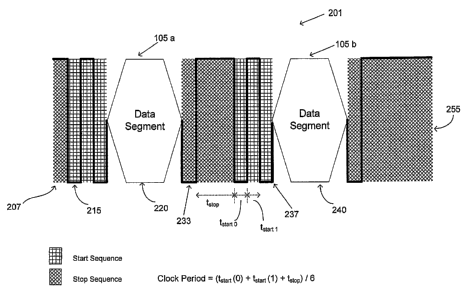
An example of a clocking period 140 is shown in Fig. lb as:
Clocking Period = (tstart(0) tstart(1) tstopY 6
[0033] Additionally, during transfer of a bit stream from, for
example, a screen
portion 503 of a computer system 500 to PAD 510, as depicted in Fig. 5, the
binary states
of the interface may correspond to the display of the screen portion 503. The
screen
portion 503 displays a black screen portion in state B and a white screen
portion in state
A. In the data structure depicted in Fig. lb, this is illustrated by a scale
150 indicating
that in state B (155) (binary 0) the screen portion 503 (Fig. 5) displays a
black screen and
in state A (152) (binary 1) the screen portion 503 displays a white screen.
[0034] Referring to Fig. 2b, a bit stream 201 includes the synchronous
one-bit
interface protocol 105 depicted in Fig. lb but repeated. For example, the
repeated
protocol 105a, 105b is used to transfer data from a screen portion 503 to a
PAD 510 such
that the bit stream is repeatedly transmitted from the screen portion 503 to
the PAD 510
as described above.
11
CA 02612978 2007-12-20
WO 2007/001944
PCT/US2006/023711
[0035] The repeated protocol 105a, 105b depicted in Fig. 2b has the
same state
parameters as in Fig. lb. The bit stream 201 of protocols 105a, 105b includes
an end
sequence 207 denoting the end of a previous bit stream, a start sequence 215
of a first
protocol 105a, a data segment 220 of the first protocol 105a, an end sequence
233 of
protocol 105a, a start sequence 237 of a second protocol 105b, a data segment
240 of the
protocol 105b, and an end sequence 255 of the second protocol 105b. The bit
stream in
Fig. 2b in the embodiment depicted in Fig. 5 provides for flashing of screen
portion 503
as follows (B denotes that the screen portion 503 displays a black screen and
W denotes
that the screen portion 503 displays a white screen portion):
io B W B Data Segment BWWWWBWB Data Segment BWWW W...
[0036] In Fig. 2b, an escape sequence for Y or more l's in a row is
transferred
during the data segment such that when there are more than Y or more l's, an
additional
1 is sent. This insures that the only time four contiguous one bits are
transferred is in a
stop sequence.
[0037] The following are examples of encoding (converting) data into a
repeated
bit stream that complies with the protocol 105, 105a, 105b depicted in Fig. lb
and Fig.
2b. In the following examples, the start sequence of the bit stream is 010 and
the stop
sequence of the bit stream is 01111. The bits between the start and stop
sequences are the
data segment which corresponds to a numerical value, e.g., 431.
Data: OxAAAA
Bit Stream: 010101010101010101001111 010101010101010101001111...
Data: 0x0431
Bit Stream: 010000001000011000101111 010000001000011000101111...
12
CA 02612978 2007-12-20
WO 2007/001944
PCT/US2006/023711
Data: OxF0F0
Bit Stream: 01011111000011111000001111 01011111000011111000001111...
[0038] Fig. 3, depicts a flow for receiving and decoding a bit stream
provided in
accordance with embodiments of the invention. For example, in the embodiment
depicted in Fig. 5, PAD 510 at the receiving end includes a data receiver
which receives
the bit stream and a computer processor (not shown) which processes and
decodes the
received bit stream. In block 310, the PAD 510 includes an optical receiver
that optically
receives the bit stream emitted from a screen portion 503 of a computer system
500 and
passes the bit stream to the processor. In block 320, the clock period is
extracted from
o the start and/or stop sequences of the bit stream as described above. In
block 330, the
data segment of the bit stream is decoded by the processor using the extracted
clock
period.
[0039] Fig. 4 depicts a flow for generating a bit stream provided in
accordance
with embodiments of the invention, and for transferring or transmitting the
bit stream. In
block 410, a processor of a computer, computer system or device determines the
clocking
information, e.g., clock period, for the bit stream. The clocking period may
be a pre-set
default clock period or a selectable or computed clock period. In block 420,
the start
sequence of the bit stream is encoded by the processor using the clock
information so as
to provide some or all of the information needed to extract a clock period
during
decoding of the bit stream. In block 430, the data segment of the bit stream
is encoded by
the processor using the clock information. In block 440, the stop sequence of
the bit
stream is encoded by the processor using the clock information, also so as to
provide
some or all of the information needed to extract a clock period during
decoding of the bit
13
CA 02612978 2007-12-20
WO 2007/001944
PCT/US2006/023711
stream. The start and stop sequences at least together provide sufficient
information for
extracting a clock period during decoding and also functioning as a start and
end for the
message or payload data 120. The encoded bit stream is transferred or
transmitted, in
block 450 by a communication device or transmitter, e.g., transferred from the
screen
portion 503 of the computer system 500 to the PAD 510.
[0040] Bit streams may be transferred or transmitted by any suitable
communication device. Similarly, bit streams may be received by any suitable
data
receiver. Transmission or transfer of bit streams may take place over any
suitable
communication link or medium, e.g., a wireless communications link.
1 o [0041] Referring to Fig. 5, as mentioned above, a personal
authentication device
(PAD) 510 is depicted receiving, e.g., an optically transmitted coded data
structure from
a computer monitor 501 of a computer system 500 in accordance with an
embodiment of
the invention. For example, the coded data structure is emitted by screen
portion 503 for
purposes of authenticating a user of a computer system 500. The computer
system 500
may communicate over a network with another computer, server, computer system
or
device. The PAD 510 includes a processor (not shown) for decoding a bit stream
and a
computer-readable storing medium storing a set of instructions for decoding
the bit
stream. The PAD 510 is useful for facilitating user access to computer system
500 or a
remote computer server, computer system or device. After the user has
initiated use of
the PAD 510, a bit stream, according to the protocol 100, 100a, 100b, 105,
105a, 105b of
the invention, is sent from screen portion 503 to the PAD 510 for
authentication
purposes. The bit streams emitted by screen portion 503 may function as an
access
challenge signal or other signal.
14
CA 02612978 2012-02-24
[0042] PAD 510 may provide a response that is then input to computer system
500
(e.g., wirelessly, by cable or by a user operated input device). Upon
verification of the
response, the user is granted access to computer system 500 or a remote
computer, server,
computer system or device. The computer system 500 includes a remote computer,
server,
computer system or device, a computer-readable storage medium storing a set or
sets of
instructions for encoding the bit stream. The PAD 510 includes a computer-
readable storage
medium storing a set or sets of instructions for decoding the bit stream.
[0043] Systems and modules described herein may comprise software, firmware,
hardware, or any combination(s) of software, firmware, or hardware suitable
for the
purposes described herein. Software and other modules may reside on servers,
workstations,
personal computers, computerized tablets, personal digital assistants (PDAs),
and other
electronic devices suitable for the purposes described herein. Software and
other modules
may be accessible via local memory, via a network, or via other means suitable
for the
purposes described herein. Data structures described herein may comprise
computer files,
variables, programming arrays, programming structures, or any electronic
information
storage schemes or methods, or any combinations thereof, suitable for the
purposes
described herein.
[0044] While the invention has been described and illustrated in connection
with
preferred embodiments, many variations and modifications as will be evident to
those
skilled in this art may be made without departing from the scope of the
invention, and the
invention is thus not to be limited to the precise details of methodology or
construction set
forth above as such variations and modification are intended to be included
within the scope
of the invention.