Note: Descriptions are shown in the official language in which they were submitted.
CA 02613105 2007-12-21
WO 2007/003208 PCT/EP2005/007085
METHOD AND SYSTEM FOR HITLESS TUNABLE OPTICAL PROCESSING
* * * * *
Field of the invention
The present invention generally relates to the field of optical
communications, in
particular to the field of optical communication systems including hitless
tunable optical
processing functionality, such as hitless tunable optical add and/or drop
multiplexing
(OADM) functionality.
Background of the invention
A common technique to increase the transmission capacity of today optical
communication systems is wavelength division multiplexing (WDM), wherein a
plurality
of optical channels, each having a respective wavelength, are multiplexed
together in a
single optical medium, such as for example an optical fiber. The WDM channels
may be
closely spaced (dense WDM or DWDM, having typical channel separation of 100
GHz -
about 0.8 nm- or 50 GHz ¨about 0.4 rim or less) or coarsely spaced (CWDM,
having
typical channel separation greater than 5 rim) or a combination thereof.
Optical networking is expected to be widely used in perspective optical
communication field. The term 'optical network' is commonly referred to an
optical system
including a plurality of point-to-point or point-to-multipoint (e.g., ring)
optical systems
optically interconnected through nodes. In all-optical transparent networks
few or no
conversions of the optical signal into electrical signal, and then again in
optical signal,
occur along the whole path from a departure location to a destination
location. This is
accomplished by placing at the nodes of the optical networks electro-optical
or optical
devices which are apt to process the optical signal in the optical domain,
with limited or no
need for electrical conversion. Examples of such devices are OADMs, branching
units,
optical routers, optical switches, optical regenerators (re-shapers and/or re-
timers) and the
like. Accordingly, the term 'optical processing' for the purpose of the
present description is
used to indicate any optical transformation given to an optical radiation,
such as optical
filtering, extracting a channel or a power portion of said channel from a set
of WDM
channels ('dropping'), inserting a channel or a power portion of said channel
into a WDM
signal ('adding'), routing or switching a channel or its power portion on a
dynamically
selectable optical route, optical signal reshaping, retiming or a combination
thereof. In
addition, optical systems, and at a greater extent optical networks, make use
of optical
1
CA 02613105 2007-12-21
WO 2007/003208 PCT/EP2005/007085
amplifiers in order to compensate the power losses due to fiber attenuation or
to insertion
losses of the optical devices along the path, avoiding the use of any
conversion of the
optical signal into the electrical domain even for long traveling distances
and/or many
optical devices along the path. In case the WDM wavelengths are closely spaced
(e.g.
within about 30 nm bandwidth around 1550 nm), all channels are typically
optically
amplified together.
In optical systems, and at a greater extent in optical networks, a problem
exists of
processing one or more optical channels at the nodes minimizing the loss
and/or the
distortion of the processed optical channel(s), as well those of the optical
channels
transmitted through the node ideally without being processed. Advantageously,
the optical
processing node should be able to simultaneously process more than one
channel, ideally
nearly all the channels. In addition, it is highly desirable that the optical
processing node is
tunable or reconfigurable, i.e., it can change dynamically the subset of
channels on which it
operates. It is highly desired that while the processing node "moves" from the
initial
channels subset (A) to the destination channels subset (B), the channels
different from A
and B (hereinafter referred to as `thru channels') remain unaffected by the
tuning
operation. In this case the component is defined as 'hitless'. In particular,
the thru channels
placed between one of the initially processed channels and the respective
final channel
after tuning should not be subject to an additional impairment penalty, called
'hit', by the
tuning operation. The hit may include a loss penalty and/or an optical
distortion such as
phase distortion or chromatic dispersion.
For example, optical communication networks need provisions for partially
altering
the traffic at each node by adding and/or dropping one or several channels out
of the total
number. Typically, an OADM node removes from a WDM signal a subset of the
transmitted channels (each corresponding to one wavelength), and adds the same
subset
with a new information content, said subset being dynamically selectable.
There are several additional concerns. The tunable optical processing node
should
not act as a narrow band filter for the unprocessed channels, since
concatenation of such
nodes would excessively narrow the channel pass bands. The tunable optical
processing
node should also have low transmission loss and low cost, since these
important factors
ultimately determine which technology is selected.
US patent 6,035,080 discloses a reconfigurable add-drop optical multiplexer (R-
ADM) including at least one reconfigurable add-drop unit that can add-drop one
channel
2
CA 02613105 2007-12-21
WO 2007/003208 PCT/EP2005/007085
out of a large set by switching the light path through one of a set of fixed
add-drop filters
(ADF). The ADFs comprise a pair of Bragg reflecting waveguides coupled
together by a
pair of spaced apart 3 dB couplers. The selection among add-drop filters is
done by sliding
an integrated optic chip with the set of ADFs between input and output
waveguides. The
sliding chip switch by itself cannot be used to reconfigure the ADM because it
will disrupt
the signal traffic as the chip is slid from one ADF to another. Instead,
before making this
change, it is desirable to switch from the add-drop filter path to a bypass
path that is off the
sliding chip without losing any bit. Reconfiguration is done by switching from
the add-
drop filter path to a bypass path, changing to a different add-drop filter and
then switching
back. In cited patent, a bypass switch is described comprising a pair of
waveguide paths
connecting a pair of identical thermo-optic switches, each one comprising a
pair of 3 dB
couplers connected by a pair of waveguide arms. Arms in first path include
heating
element to control the arm optical path-length (and thus phase). Arms in
second path can
provide a phase shift of 7r as compared with unheated arms in first path. In
operation, the
thermo-optic switches determine which path input light will take. During
switching from
one path to another, the lightwave separates into two paths, and these
contributions
interfere when the two paths come together again. Thus the transmission
depends on the
phase difference of the two paths. According to the cited patent, the phase
delay of the
bypass path is adjusted to maintain nearly maximum transmission during
switching via a
phase shifter placed in the bypass path. A number of such low loss
reconfigurable ADM
units can be put in series to independently add and drop that number of
channels out of a
larger set.
The Applicant has noted that the ADM described in the cited patent is not
really
hitless, in that there is a loss of about 1 dB in the channels neighboring the
add-dropped
channel during switching between the first and second paths (Figure 11 of
cited patent). An
optical field with frequency near the stop band of the Bragg reflectors will
undergo a phase
change significantly different from a field with frequency far from the stop
band (Figure 10
of cited patent).
In patent application US 2005/0031260 it is described, with reference to
figure 4, a
variable optical delay line comprising a continuous delay element having two
variable
delay arms. The first arm comprises a 0 to T continuous delay and the second
arm
comprises both a 0 to T continuous delay and a fixed delay T.
The Applicant has found that there is a need for an optical communication
system
3
CA 02613105 2007-12-21
WO 2007/003208 PCT/EP2005/007085
having optical processing functionality which is tunable and hitless. In
particular, the hit
loss during tuning should be less than or equal to 1 dB. Moreover, the optical
processing
node should leave unaltered the thru channels during tuning. In particular, it
is desired that
the optical processing node introduces no or low chromatic dispersion to the
thru channels.
In addition, the optical processing node should preferably leave unaltered the
unprocessed
channels during processing operation and should be low-loss, low-cost, fast
tunable and/or
broadband.
Summary of the invention
The Applicant has found a method and a system for optical transmission
furnished
of optical processing functionality which can solve one or more of the
problems stated
above. In particular these method and system comprise optical processing
capabilities
which are hitless and tunable. The solution of the present invention is
simple, feasible and
low cost.
The optical processing functionality according to the present invention is
based on a
scheme for hitless switching between two optical paths, such scheme comprising
a first
1x2 optical switch (or tunable coupler) adapted to address the WDM signal from
one input
waveguide to one of two possible optical paths. A second 2x1 optical switch
(or tunable
coupler) synchronized with the first one is adapted to collect the WDM signal
coming from
said one of the two possible optical paths and to address it to an output
waveguide. The
switching function can be implemented using known approaches, such as Mach-
Zehnder
interferometers (MZI), variable Y branches, variable couplers, variable
polarization
rotators/splitters, etc. A tunable filter (processing device) is placed on the
first of the two
optical paths (operating path).
During the filtering operation of a given channel A, the first switch
addresses
substantially the whole WDM signal to travel through the operating optical
path, and the
second switch collects the WDM signal from said optical path and addresses it
to output
waveguide (State 1). Before starting the tuning operation of the tunable
filter, the two
switches are reverted, so that substantially the whole WDM signal is addressed
(State 2) to
the second optical path (bypass path). During the transition from State 1 to
State 2 the
WDM signal is split between the two possible optical paths and is recombined
into the
output waveguide, advantageously without any losses of power and, preferably,
without
any optical distortion.
4
CA 02613105 2007-12-21
WO 2007/003208 PCT/EP2005/007085
The Applicant has found that it is important to keep a correct phase relation
between the
fraction of the WDM signal that travels through the first optical path and the
fraction that
travels through the second optical path, otherwise a non negligible amount of
optical power
that should be recombined by the second optical switch and addressed to the
output
waveguide, could be lost during the transition from State 1 to State 2.
The tunable optical filter along the first optical path typically introduces a
perturbation in the phase response at the wavelengths adjacent to the filtered
one.
The Applicant believes that a problem exists of maintaining the correct phase
relationship between the two optical paths, especially at thru wavelengths
adjacent to the
The Applicant has found that to keep in phase the signal at all the
wavelengths
(except, typically but not necessarily, the filtered one) while they are split
between the two
optical paths, it is convenient to balance on the bypass path the phase
perturbation
introduced by the filter on the operating path.
The Applicant believes that the present invention solves the above problem of
maintaining a correct phase relationship between the two optical paths being
based on a
resonant all-pass filter placed along the bypass path and configured to
compensate the
phase distortion introduced by the filter on the operating path, at least at
WDM channels
adjacent to the filtered one, while keeping unaffected the amplitude response
of the signal
In this way at any wavelength (except possibly the filtered one) the portion
of
signal that travels through the operating path is kept in phase with the
portion of signal that
travels through the bypass path, and the signal is entirely recombined by the
second switch
The Applicant has found that the hitless path switch scheme and method
described
above may be advantageously applied to a method for hitless tuning the tunable
filter
optically coupled to the operating path. Accordingly, when the path switch
scheme is in
5
CA 02613105 2013-04-24
State 2, the optical filter on the first path is tuned from the initial state
of filtering (e.g.
extracting) channel A to the final state of filtering channel B. The entire
input signal is directed
through the second path during adjustment of the optical filter, until the end
of the tuning.
In addition, one of the resonant wavelengths of the all pass filter is tuned
from the initial
wavelength A to the final one B. During this operation the resonant wavelength
of the all-pass
filter comes across all the thru channels that are comprised between A and B.
Advantageously,
the all pass filter, whose chromatic dispersion arises from the resonance, is
configured such that
the extra chromatic dispersion added to the thru channels in between the range
of tuning is
negligible with respect to the standard WDM system requirements.
At the end of the tuning operation the switches are reverted to State 1 and
consequently
the WDM signal is re-addressed to the first optical path and the tunable
filter.
According to an aspect of the present invention, there is provided a method
for switching
from a first optical path optically coupled to an optical processing device to
a second optical
path. The first and second optical paths optically connect, in parallel
configuration, a first optical
switch to a second optical switch. The method comprises: directing a
wavelength-division
multiplexed (WDM) optical signal comprising at least a first operating
wavelength through the
first optical path to the optical processing device, which is tuned to the
first operating
wavelength; tuning a resonant all-pass filter optically coupled to the second
optical path to have
a resonant wavelength corresponding to the first operating wavelength so as to
match, at least at
a wavelength adjacent to the first operating wavelength, a phase distortion
introduced by the
optical processing device on the optical radiation, the resonant all-pass
filter having a
wavelength-independent amplitude transfer function in a wavelength band
including the WDM
optical signal; and synchronously actuating the first and the second optical
switches so as to
switch the optical radiation from the first optical path to the second optical
path.
Preferably, in the step of tuning the resonant all-pass filter, a resonant
wavelength of the
resonant all-pass filter is made equal to the first operating wavelength and,
more preferably, the
optical processing device has a resonant wavelength equal to the first
operating wavelength.
Advantageously, the resonant all-pass filter comprises a single resonator.
This simplifies
fabrication processing and, more important, helps reducing the chromatic
dispersion introduced
by the all-pass filter.
6
CA 02613105 2013-04-24
More advantageously, the optical processing device comprises a plurality of
filtering
stages, each stage being coupled to the first optical path via a respective
power coupling
coefficient, and wherein the power coupling coefficient between the single
resonator of the all-
pass filter and the second optical path is selected to be equal to the sum of
the power coupling
coefficients of the plurality of filtering stages of the optical processing
device.
Preferably, the resonant all-pass filter comprises micro-ring or racetrack
resonators.
Typically the optical processing device is a tunable optical add and/or drop
filter.
In one embodiment, the method above further includes the step of shutting off
the first
operating wavelength.
According to another aspect of the present invention, the method further
includes, after
the step of synchronously actuating the first and the second optical switch,
the steps of: tuning
the optical processing device to a second operating wavelength; tuning the
resonant all-pass filter
so that a resonant wavelength of the resonant all-pass filter is made equal to
the second operating
wavelength; and synchronously actuating the first and the second optical
switches so as to switch
the optical radiation from the second optical path to the first optical path.
In one embodiment, the second operating wavelength is shut off.
According to another aspect of the present invention, there is provided an
optical
processing node comprising: a first optical switch having an input port and a
first and second
output ports; and a second optical switch having first and second input ports
and an output port,
wherein the first and second optical switches are configured to be actuated
synchronously; a first
optical path optically connecting the first output port of the first optical
switch to the first input
port of the second optical switch; a second optical path optically connecting
the second output
port of the first optical switch to the second input port of the second
optical switch; a tunable add
and/or drop filter optically coupled to the first optical path and comprising
an optical port
configured to drop or add at least a first operating wavelength of a
wavelength-division
multiplexed (WDM) optical signal propagating through the first optical path;
and a resonant all-
pass filter optically coupled to the second optical path and being tunable to
have a resonant
wavelength corresponding to the first operating wavelength so as to match a
phase distortion
which the add and/or drop filter introduces on an optical radiation
propagating through the first
optical path, the resonant all-pass filter having a wavelength-independent
amplitude transfer
function in a wavelength band including the WDM optical signal.
7
CA 02613105 2013-10-11
,
According to another aspect of the present invention, there is provided
optical
processing node comprising: a first optical switch having an first input port
and first
and second output port and a second optical switch having a respective first
and second
input port and a first output port, wherein the first and second optical
switches are
configured to be actuated synchronously; a first optical path optically
connecting the
first output port of the first optical switch to the first input port of the
second optical
switch; a second optical path optically connecting the second output port of
the first
optical switch to the second input port of the second optical switch; a
tunable optical
processing device optically coupled to the first optical path configured to
process at least
a first operating wavelength of a wavelength-division multiplexed (WDM)
optical signal
propagating through the first optical path; and a resonant all-pass filter
optically coupled
to the second optical path; wherein the resonant all-pass filter comprises a
single
resonator, and is tunable to have a resonant wavelength corresponding to the
first
operating wavelength so as to match a phase distortion which the tunable
optical
processing device introduces on an optical radiation propagating through the
first optical
path, the resonant all-pass filter having a wavelength-independent amplitude
transfer
function in a wavelength band including the WDM optical signal.
In a still further aspect, an optical communication system comprises a
transmitter,
a receiver, an optical line optically connecting the transmitter and the
receiver and an
optical processing node as described above.
Preferably, the resonant all-pass filter may be adapted to be tuned so as to
compensate a phase distortion which the add and/or drop filter is apt to
introduce on an
optical radiation propagating through the first optical path.
The resonant all-pass filter may comprise a resonant cavity and, more
preferably,
it may comprise a single resonator.
The tunable add and/or drop filter advantageously may comprise a plurality of
filtering stages, each stage comprising a resonant cavity optically coupled to
the first
optical path via a respective power coupling coefficient, and the power
coupling
coefficient between the single resonator of the resonant all-pass filter and
the second
7A
CA 02613105 2013-10-11
,
,
optical path is selected to be equal to the sum of the power coupling
coefficients of the
plurality of filtering stages of the tunable add and/or drop filter.
The resonant all-pass filter may be configured to introduce to an optical
signal
propagating therethrough a dispersion of less than or equal to 100 ps/nm in
absolute
value.
The resonant all-pass filter in one preferred embodiment comprises micro-ring
or
racetrack resonators.
Brief description of the drawings
The features and advantages of the present invention will be made clear by the
following detailed description of an embodiment thereof, provided merely by
way of
non-limitative example, description that will be conducted making reference to
the
annexed drawings, wherein:
8
CA 02613105 2007-12-21
WO 2007/003208 PCT/EP2005/007085
Figure 1 schematically shows in terms of functional blocks an exemplary
optical
communication system architecture according to the present invention;
Figure 2 is a schematic diagram showing in terms of functional blocks an
exemplary configuration of a scheme for switching an optical path according to
the present
invention;
Figure 3 is a schematic diagram showing in terms of functional blocks an
exemplary configuration of a hitless add and/or drop device according to the
present
invention;
Figures 4a and 4b show respectively amplitude and phase response of the
add/drop
filter comprised in the add/drop device of Figure 3;
Figures 5a-d show respectively amplitude, phase, group delay and dispersion
spectrum of the resonant all-pass filter comprised in the add/drop device of
Figure 3;
Figures 6a and 6b show respectively a comparison and the difference of the
phase
responses shown in Figures 4b and 5b;
Figure 7 shows calculated results of the hit loss of the add/drop device of
Figure 3;
and
Figure 8 shows calculated results of the hit loss of a comparative add/drop
device
which does not make use of the present invention.
Detailed description of the preferred embodiment(s) of the invention
Figure 1 shows an optical communication system architecture according to a
possible embodiment of the present invention.
The optical communication system 100 comprises at least a transmitter 110, a
receiver 120 and an optical line 130 which optically connects the transmitter
and the
receiver. The transmitter 110 is an opto-electronic device apt to emit an
optical signal
carrying information. It typically comprises at least an optical source (e.g.,
a laser) apt to
emit an optical radiation and at least a modulator apt to encode information
onto the optical
radiation. Preferably, the transmitter 110 is a WDM transmitter (e.g., either
DWDM or
CWDM) and the optical signal comprises a plurality of optical wavelengths each
carrying
modulation-encoded information. The receiver 120 is a corresponding opto-
electronic
device apt to receive the optical signal emitted by the transmitter and to
decode the carried
information. The optical line 130 may be formed by a plurality of sections of
optical
transmission media, such as for example optical fiber sections, preferably
cabled. Between
9
CA 02613105 2007-12-21
WO 2007/003208 PCT/EP2005/007085
two adjacent sections of optical fiber, an optical or opto-electronic device
is typically
placed, such as for example a fiber splice or a connector, a jumper, a planar
lightguide
circuit, a variable optical attenuator or the like.
For adding flexibility to the system 100 and improving system functionality,
one or
a plurality of optical, electronic or opto-electronic devices may be placed
along the line
130. In figure 1 a plurality of optical amplifiers 140 are exemplarily shown,
which may be
line-amplifier, optical booster or pre-amplifier.
According to the present invention, the optical system 100 comprises at least
one
optical processing node (OPN) 150 optically coupled to the optical line 130
and apt to
filter or route or add or drop or regenerate, fully or partially, at least one
optical
wavelength of the WDM optical signal propagating through the optical line 130.
The OPNs
are preferably dynamically tunable or reconfigurable (TOPN). In the particular
case
wherein the optical processing node 150 is an optical add/drop node 150, as
shown in Fig.
1, i.e., a node adapted to route or switch or add and/or drop, the routed or
switched or
dropped or added wavelength(s) may be received or transmitted by further
receiver(s) 152
or transmitter(s) 154, respectively, which may be co-located with the OPN node
or at a
distance thereof. The optical system or network 100 may advantageously
comprise a
plurality of optical processing nodes. In Figure 1 a further optical
processing node 150' is
exemplarily shown, together with its respective optional transmitting and
receiving devices
152' and 154'.
An optical system 100 having optical add/drop nodes 150, as shown in Figure 1,
is
commonly referred to as an optical network and it is characterized by having a
plurality of
possible optical paths for the optical signals propagating through it. As
exemplarily shown
in Figure 1, a number of six optical paths are in principle possible, which
corresponds to
all possible choices of the transmitter-receiver pair in Figure 1 (excluding
the pairs
belonging to the same node).
According to the present invention, the tunable optical processing node 150 is
hitless, being based on a hitless path switch scheme comprising a bypass path
which, in
turn, includes a resonant all-pass filter.
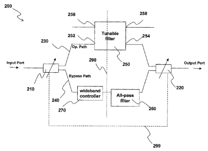
Figure 2 shows a schematic diagram of a hitless path switch scheme 200 in
accordance with an embodiment of the present invention.
, The general design scheme of the present invention, shown in Figure 2,
comprises
a first optical switch 210 with an input port and a first and a second output
port and a
CA 02613105 2007-12-21
WO 2007/003208 PCT/EP2005/007085
second optical switch 220 having a first and a second input port and an output
port.
Throughout the present description, the terms 'input' and 'output' are used
with reference
to a conventional direction of propagation of the optical radiation (in Fig. 2
exemplarily
from left to right), but, when in operation, the optical radiation may
propagate in any
direction. A first optical path 230 and a second optical path 240 optically
connect in
parallel configuration the first optical switch 210 to the second optical
switch 220. The first
optical path 230 (called 'operating path') connects first output port of the
first optical
switch 210 to first input port of the second optical switch 220. The second
optical path 240
(called 'bypass path') connects second output port of the first optical switch
210 to the
second input port of the second optical switch 220. The two optical paths 230
and 240 are
preferably optically separated unless in correspondence of the optical
switches 210 and
220.
The first optical switch 210 is a splitting device configured to assume
alternatively
a first and a second state, wherein an optical radiation inputted in the input
port is directed,
in the first state, substantially solely to the first output port and, in the
second state,
substantially solely to the second output port. Preferably, the optical switch
210 switches
from the first to the second state continuously, i.e. the splitting ratio of
the output power of
the two output ports switches from 0:100 to 100:0 and vice versa continuously.
The second
optical switch 220 has the same optical behavior of the first optical switch
210, provided
that its output port takes the place of the input port of the first optical
switch and its first
and second input port take the place of the first and second output ports of
the first optical
switch. In other words, the second switch 220 is a "time-reversal copy" of the
first optical
switch 210, i.e. it operates in reverse with respect to the first switch. In
one advantageous
configuration, the second optical switch 220 is a structurally identical copy
of the first
optical switch 210 operating in reverse, i.e the second optical switch 220 is
a mirror
symmetric copy of the first optical switch 210 with respect to the vertical
dashed axis 298
in Fig. 2.
The first and second optical switch 210, 220 may be any arbitrary device that
meet
the above requirements, including variable couplers (such as planar waveguide
couplers),
variable Y branches, variable polarization rotators/splitters, 6,13 switches,
alternating 643
switches, Mach-Zehnder interferometer (MZI) based switches or the like. The
first and
second optical switch 210, 220 are preferably wavelength-independent over the
wavelength band of interest. Typically, the two optical switches are such that
the optical
11
CA 02613105 2007-12-21
WO 2007/003208 PCT/EP2005/007085
radiations inputted in the first and in the second optical path have the same
polarization or
at least are not orthogonally polarized.
The first and the second optical switch 210 and 220 are configured to be
operated in
synchronous, as schematically shown in Fig 2 by the dashed line 299, so as to
maintain at
any time during operation a symmetrical configuration of the path switch
scheme 200. The
two optical switches 210, 220 may be actuated by any actuation technique (such
as thermo-
optic, MEMS actuated, electro-optic, acusto-optic, elasto-optic, stress, etc)
so as to switch
from the first to the second state and vice versa.
According to the present invention, a tunable optical processing device 250 is
optically coupled to the first optical path 230 and it is adapted to receive
at least a portion
of the optical radiation propagating through the first optical path 230 via an
input port 252
and to output a transformed optical radiation via an output port 254 (called
`thru port' 254).
The tunable optical processing device 250 may be any optical device adapted to
give an
optical transformation to the optical radiation propagating across it from the
input port 252
to the thru port 254, being the optical transfer function wavelength-dependent
in the
wavelength band of interest. In the present description, any physical quantity
which
substantially changes within the optical wavelength band of interest (e.g. 30
nm around
1550 nm) is referred to as being 'wavelength-dependent'. Conversely, a
physical quantity
which does not substantially change within the optical wavelength band of
interest is
referred to as being 'wavelength-independent'. In a preferred configuration,
the tunable
optical processing device 250 is a resonant optical device, i.e. it comprises
an interference
region having one or more resonant wavelengths, defined as those wavelengths
which
interfere constructively in the interference region. The distance between two
adjacent
resonant wavelengths is called free spectral range (FSR). In preferred
configurations, the
interference region comprises a resonant optical cavity wherein the resonant
wavelengths
fit an integer number of times on the cavity length comprised in the resonant
optical cavity.
For example, the resonant optical processing device 250 may comprise linear
cavities (i.e.
cavities each having a plurality of reflectors), microrings, racetracks, Bragg
gratings,
photonic band gap cavities, etc. In a preferred configuration, the resonant
optical
processing device 250 comprises microring or racetrack resonators. The
transfer function
of the resonant optical processing device 250 is typically characterized by
strong
wavelength dependence at and in the proximity of a resonant wavelength.
Typically, the
wavelength currently processed by the optical processing device 250
corresponds to one of
12
CA 02613105 2007-12-21
WO 2007/003208 PCT/EP2005/007085
its resonant wavelengths.
In the particular embodiment wherein the path switch scheme 200 is comprised
within an optical add/drop node 150, as exemplarily shown in Fig. 1, the
optical processing
device 250 is an optical add and/or drop filter (OADF) having at least a
further optical port
256 ('drop port' 256) having the function of routing or dropping or adding,
fully or -
partially, at least an optical wavelength within the optical band of interest
propagating in
the operating path 230. In a preferred embodiment, the OADF 250 has a still
further optical
port 258 ('add port' 258) which in combination with the further optical port
256 forms a
pair of add and drop ports.
According to the present invention, a resonant all-pass optical filter 260 is
optically
coupled to the bypass path 240 and it is adapted to introduce a narrowband
wavelength
= dependent phase change so as to match the phase distortion introduced by
the tunable
optical processing device 250 at least at a wavelength neighboring the
wavelength
processed by the optical processing device 250. In the present description, a
resonant all-
pass filter is defined as an optical filter having, in the wavelength band of
interest, a
wavelength independent amplitude transfer function and a phase transfer
function having a
wavelength/frequency dependence which exhibits typical resonance induced
behavior. The
resonant all-pass filter 260 comprises a resonant optical cavity having one or
more
resonant wavelengths. The all-pass filter 260 is preferably tunable. Strong
wavelength
dependence of the phase transfer function typically occurs in correspondence
of the
resonant wavelength(s). Advantageously, the resonant all-pass filter 260 is
adapted to be
tuned to have at least a resonant wavelength in correspondence of a resonant
wavelength of
the tunable optical processing device 250 on the opposite path 230.
Advantageously, the
all-pass filter 260 is adapted to have a FSR selectable to be equal to the FSR
of the tunable
optical processing device 250 so as to facilitate fabrication and phase
matching.
The resonant all-pass filter 260 is adapted to apply the correct phase
distortion on
channels adjacent to the processed one while leaving substantially unaffected
the signal
amplitude. Preferably the all-pass filter 260 is designed not to introduce
appreciable
chromatic dispersion on the channels crossing it, especially on the thru
channels upon
tuning. The maximum chromatic dispersion introduced by the filter 260 on thru
channels,
in absolute value, is advantageously less than 100ps/nrn, more preferably less
than
20ps/nm. In a preferred embodiment the all-pass filter 260 comprises a single
resonator
optically coupled to the bypass path 240 with a suitable coupling coefficient
between the
13
CA 02613105 2007-12-21
WO 2007/003208 PCT/EP2005/007085
single resonator and the optical bypass path 240. In the particular embodiment
wherein the
tunable optical processing device 250 is comprised of a plurality of resonator-
based stages,
each stage being coupled to the operating optical path 230 via a respective
power coupling
coefficient, the all-pass filter 260 preferably comprises a cascade of stages
each comprising
a single resonator optically coupled to the bypass path 240 with a suitable
coupling
coefficient between the single resonator and the optical bypass path 240. The
number of
stages of the all-pass filter 260 may be equal to the number of stages of the
processing
device 250 or, advantageously, less than that number. In a preferred
configuration, the all-
pass filter 260 comprises a single resonator having the power coupling
coefficient between
this single resonator and the bypass path 240 advantageously selected to be
equal to the
sum of the power coupling coefficients of the stages of device 250. The
Applicant has
found that placing a single resonator all-pass filter 260 with the above
characteristics helps
minimizing the chromatic dispersion introduced by the all-pass filter. In
fact, the Applicant
has found that the chromatic dispersion introduced by a single ring-resonator
all pass filter
typically reduces when the ring to bus waveguide coupling coefficient
increases. The
criterion for assessing the suitable coupling coefficient of the all pass
filter is that it has to
be equal to the sum of the coupling coefficients along the operating path.
A wideband optical phase controller 270 is preferably placed along the second
optical path 240 and it is adapted to give in a controlled way a wideband
phase change to
the optical radiation propagating through the second optical path so as to
maintain the
overall phase balance between the first and the second optical path. The
wideband optical
phase controller 270 is functionally different from the narrowband all-pass
optical filter
260 in that the phase transfer function of the optical phase controller 270 is
substantially
constant in the wavelength band of interest. In particular, the phase transfer
function of the
phase controller 270 has a wavelength dependence which exhibits a change less
than 5
degrees on a bandwidth of at least 32 nm. For example, the wideband optical
phase
controller may be a waveguide phase shifter having a nearby electrode to
adjust the phase
by electro-optic effect or a nearby micro-heater to adjust the phase by thermo-
optic effect.
It is noted that the phase shifter of the prior art patent US 6,035,080 is of
the same type of
the wideband optical phase controller 270.
A method based on the hitless path switch scheme 200 of Figure 2 for hitless
switching from a first optical path 230 optically coupled to an optical
processing device
250 to a second optical path 240 in accordance to the present invention will
be described in
14
CA 02613105 2007-12-21
WO 2007/003208 PCT/EP2005/007085
the following. Reference will be made to elements and corresponding reference
numerals
of Figure 2.
As a starting point, during optical processing operation a WDM optical signal
is
directed, through the operating path 230, to the optical processing device 250
which
processes at least a channel of the WDM spectrum. This may be accomplished by
acting on
the optical switches 210 and 220 so as to direct substantially all the optical
radiation
inputted in the input port of the optical switch 210 into the first output
port of switch 210
optically connected to the first optical path 230 and to direct substantially
all the optical
radiation received in the first input port of the optical switch 220 into the
output port of
switch 220.
A resonant all-pass filter 260 optically coupled to the second optical path
240 is
tuned so as to match the phase distortion introduced by the optical processing
device 250
placed along the first optical path 230, at least in correspondence of the WDM
wavelengths
neighboring the processed one. This phase matching is achieved at least for
the two
channels immediately adjacent the processed one and, preferably, for the
further two
channels adjacent the latter two. Typically, no phase matching is achieved at
the processed
wavelength. The tuning may be accomplished by any suitable technique such as
thermo-
optic, electro-optic, acousto-optic, MEMS actuated, elasto-optic and the like.
In a preferred
configuration, wherein the processing device 250 has resonant wavelengths, the
all-pass
filter 260 is tuned until one of its resonant wavelengths is equal to one of
the current
resonant wavelengths of the optical processing device 250. Advantageously,
said current
resonant wavelength corresponds to the processed wavelength.
Once the resonant all-pass filter 260 is properly tuned, the first and the
second
optical switch 210 and 220 may be synchronously switched so as to direct the
WDM signal
from the first optical path to the second optical path. In all the
intermediate states during
the switching operation, the two portions of WDM signal propagating
respectively along
the = two optical paths remain in a phase relationship which is suitable to
properly
recombine in the second optical switch 220 so as to be entirely outputted in
the output port
of the second optical switch without loss and/or distortion. Typically, the
processed
wavelength, which may not be phase matched and thus may suffer an hit, is
turned off
before or during the path switch or it is neglected by the optical
communication system
100 during the switch.
In one embodiment of the present invention, the hitless path switch method
CA 02613105 2007-12-21
WO 2007/003208 PCT/EP2005/007085
described above may be used, according to the following steps, within a method
for hitless
tuning an optical processing device 250 from an initial processing wavelength
Xi to a final
processing wavelength X.2, both belonging to a WDM signal, wherein said
optical
processing device 250 is placed along the first optical path 230.
Advantageously, said
method is applied to tune an optical add and/or drop filter 250, without any
power loss
and/or distortion on thru channels during tuning operation. Preferably, the
thru channels
are also subject to low chromatic dispersion during the entire tuning
operation of the
optical processing device 250.
In the initial operating condition, a WDM signal comprising the initial
wavelength
k1 is directed via the first optical path 230 to the optical processing device
250 which is
tuned to process the initial wavelength. During this processing state, the
whole WDM
signal is addressed by first switch 210 into first optical path 230. For
example, in the case
wherein a tunable add/drop filter 250 is placed along the first optical path,
it may extract ki
via the drop port 256 and optionally add the same wavelength with a new
information
content through the add port 258, as is known in the art. The channels
centered at
wavelengths different from X1 may travel through first path 230 without any
substantial
power loss, and may be addressed, possibly together with the added channel, by
the second
switch 220 to output port. As explained above, the channels adjacent to the
processed one
(k1) typically suffer a certain phase distortion, due to the presence of the
tunable
processing device 250.
Optionally and advantageously, the initial and final processing wavelengths,
ki,
are preferably shut off before or at a certain stage of the tuning operation
of the optical
processing device 250.
The resonant all pass filter 260 on bypass optical path 240 is tuned so as to
match
the phase distortion of the optical filter 250 placed along the first optical
path 230 on the
channels adjacent to Xi, as explained above. Preferably, the resonant all-pass
filter 260 is
made to resonate at the initial wavelength ki.
After the tuning of the all-pass filter 260, the first and the second optical
switch
210, 220 are synchronously switched so as to direct the WDM signal from the
first optical
path 230 to the second optical path 240. The reverting operation typically
requires few
milliseconds (between about 0.5 and 2 ms), and during this period of time the
thru
channels remain addressed to the output port of the second switch 220, without
any
16
CA 02613105 2007-12-21
WO 2007/003208 PCT/EP2005/007085
substantial power loss. For example, if the tunable filter 250 and the all-
pass filter 260 are
both tuned at the same resonant wavelength ki, the fraction of signal
traveling through
operating path 230 is affected by the same phase distortion as the fraction
traveling trough
bypass path 240, and the whole optical power is correctly recombined by the
second switch
220 into its output port. At the end of the switching operation the whole WDM
signal is
addressed by first switch 210 into second optical path 240, where the all pass
filter 260 is
placed.
By some physical excitation (thermo-optic, electro-optic, stress...) the
tunable
processing device 250 is then adjusted to process (e.g. extract and/or insert)
the new
channel centered at the final wavelength X2. To keep the correct phase
relationship between
optical paths 230 and 240, also the all pass filter 260 is tuned to resonate
at k2. In tuning
the all pass filter 260 from Xi to X,2, it will resonate at all the thru
wavelengths between Xi
and k2. But, as described above, the all pass filter 260 is advantageously
configured to
introduce negligible losses and, preferably, negligible chromatic dispersion
on its resonant
wavelength and the adjacent ones, and so the thru channels remain
substantially unaffected
by the all pass filter tuning.
At the end of the tuning operation the first and the second optical switch
210, 220
are gradually synchronously reverted to the initial condition, i.e. to direct
the WDM signal
from the second optical path 240 back again to the first optical path 230.
During this
switching phase, since the tunable processing device 250 and the all pass
filter 260 are both
tuned at the same wavelength X,2, the fraction of signal traveling trough path
230 is affected
by the same phase distortion as the fraction traveling trough path 240, and
the whole
optical power is correctly recombined by the second switch 220 into its output
port.
At the end of the switching operation all the WDM signal is addressed by
switch
210 again into optical path 230, where the optical processing device 250 may
now process
the new wavelength k2. In case the channels at Xi and X,2 were shut off, now
they can be re-
switched on. In case of an OADF 250, in the final operating condition it
extracts k2 from
the drop port 256 and possibly adds it with a new information content to the
add port 258.
During the entire operation, the thru channels remain substantially
unaffected.
With reference now to Figure 3, an exemplary realization of a tunable hitless
optical add and/or drop multiplexing device 300 in accordance with the present
invention
will now be described. Where appropriate, the same reference numerals of
Figure 2 for
17
CA 02613105 2007-12-21
WO 2007/003208 PCT/EP2005/007085
like elements have been used and, for these elements, reference is made to the
description
above.
The first and second optical switch 310, 320 are identical MZI-based optical
switches, each comprising a balanced MZI having a pair of identical 3-dB
optical couplers
312 and a controllable phase shifter 314 (for example thermally actuated)
along the arm
corresponding to the first optical path 230.
The tunable optical add and/or drop filter (OADF) 350 on the operating path
230 is
a resonant-type optical filter comprising microring resonators 352, 352' and
352". In the
exemplary embodiment of Fig. 3, the tunable OADF 350 comprises three stages
352, 352'
and 352", each stage comprising three series-coupled microring resonators. The
first stage
352 is adapted to drop a wavelength from the first optical path 230 and the
third stage
352" is adapted to add a further wavelength, preferably equal to the dropped
wavelength,
into the first optical path 230. Middle stage 352' is adapted to clean the
thru channels.
Exemplarily, a third order Chebyshev optical filter 350 has been
advantageously
designed to meet the following specifications: FSR greater than or equal to
about 4 THz
(32 run at 1550 urn), passband (at drop port 256) greater than or equal to
about 30 GHz
with ripple less than about 0.15dB, extinction (at drop port 256) on adjacent
WDM
channels (100 GHz spacing) greater than or equal to about 30 dB, rejection (at
thra port
254) for the filtered channel greater than or equal to about 30 dB.
The three stages are identical. Within each stage, the power coupling
coefficients of
the couplers between bus-waveguides and microring-waveguides (couplers 354)
are equal
to about 5.06% and the power coupling coefficients of the couplers between
adjacent rings
(couplers 356) are equal to about 0.066%.
The OADF 350 can be realized by any known optical material system, such as
exemplarily silicon waveguides buried in a Si02 cladding. This latter high
index contrast
waveguide allows fabricating microring resonators with very small radius and
negligible
bending losses. Small ring radius (e.g. not greater than about 31am)
advantageously gives
large FSR, preferably larger than 32nm (equal to 4THz at about 1550 nm,
suitable for 40
WDM channels 100GHz-spaced in C-band). In this exemplary embodiment, the bus
and
the ring waveguides are about 450 nm wide and about 220 nm high, the ring
radius is about
2.7 pm, the bus to ring gap is about 100 nin wide and the ring to ring gap is
about 400 nm
wide.
The OADF 350 may be thermally tuned by micro-heater placed above the
18
CA 02613105 2007-12-21
WO 2007/003208 PCT/EP2005/007085
microrings, over the Si02 upper cladding.
In Figures 4a and 4b there are respectively shown the calculated amplitude
(thru
port 254 and drop port 256) and phase (thru port 254) response of the three
stage add
and/or drop filter 350 described above.
In accordance with the present invention, a tunable resonant all-pass filter
360
placed along the bypass path 240 is adapted to be tuned to match the phase
distortion
introduced by the optical filter 350 and shown in Fig. 4b.
In one embodiment the all pass filter 360 comprises a single microring
resonator
362, with FSR substantially equal to the FSR of the tunable OADF 350 and
having bus-to-
ring power coupling coefficient substantially equal to the coupling
coefficient of a single
stage of the OADF 350 (e.g. 5.06% in the example above) times the number of
stages of
the OADF 350 (three in the example above). The resulting power coupling
coefficient is
equal to about 16%. Exemplarily, the ring waveguide is about 450 nm wide and
about 220
urn high, the ring radius is about 2.7 gm, the bus to ring gap is about 40 urn
wide. Using, in
place of the microring resonator 362, a racetrack having the section of
straight waveguide
coupled to the bus-waveguide 240 of about 950 nm of length and a radius of
curvature of
about 2.4 pm, it is possible to increase the gap to about 90 urn.
The amplitude and phase response of the all-pass filter 360 described above
have
been evaluated by a transfer matrix method and are plotted in Figure 5a and
5b,
respectively, for a frequency range corresponding to the first four channels
(on each side)
adjacent to the filtered one (100 GHz spacing). It is noted that the all-pass
filter introduces
no extra losses on the channels (Fig. 5a) and that a phase excursion of about
250 degrees is
experienced in a narrow band of about 200 GHz (Fig. 5b).
In Figure Sc and 5d the corresponding group delay and chromatic dispersion
introduced by the above all-pass filter 360 are respectively plotted. The
maximum value of
chromatic dispersion introduced by the exemplary all-pass filter 360 is about
7ps/nm;
which is a value widely acceptable in most WDM systems.
In Figure 6a the phase responses of the above described tunable OADF 350 and
all-pass filter 360 are compared. In Figure 6b the corresponding difference
between the
phase perturbations along the two optical paths 230, 240 is plotted. The phase
difference
remains in the range of few degrees (no greater than about 5 degrees) for the
four channels
adjacent to the filtered one. The same holds for the four channels on the
opposite side with
respect to the filtered one.
19
CA 02613105 2013-04-24
In Figure 7 it is shown the calculated (transfer matrix technique) power (in
units of 10-3
dB) at the output port of the second optical switch 320 of the OADM device 300
of Figure 3 for
the four channels adjacent to the filtered one on one side (respectively 100
GHz, 200 GHz, 300
GHz, 400 GHz apart from resonant frequency) during the transition from bypass
state (signal
traveling through bypass path 240) to processing state (signal traveling
through operating optical
path 230) in presence of the phase compensation by the single ring all-pass
filter 360. The
horizontal axis shows the phase shift introduced by the phase shifter 314 of
Fig. 3, wherein a null
phase shift corresponds to the bypass state, while a 180 phase shift
corresponds to the
processing state. The four channels adjacent to the filtered one suffer a
power loss less than or
equal to about 0.002 dB (0.5%o) during transition from second optical path to
first optical path
(and vice versa). This amount of loss is tolerable in most WDM systems and
represents a great
improvement with respect to prior art solutions.
As a comparative example, in Figure 8 it is shown the calculated power at the
output port
of the second optical switch 320 for the four adjacent channels during the
same switching
transition of Fig. 7, now without compensation of the phase distortion, i.e.,
without the all-pass
filter 360. It is noted that the wideband phase controller 270 is present and
maintains the
wideband phase balance between the two optical paths. The channel adjacent to
the filtered one
suffers a loss of about 1.3 dB during switching transition from second path to
first path and vice
versa. This amount of power loss is not tolerable in nowadays WDM systems.
Although some embodiments have been described, it may be apparent to those
skilled in
the art that several modifications to the described embodiments, as well as
other embodiments
are possible. The invention, rather, is defined by the claims.